
Black Silicon: Breaking through the Everlasting Cost vs. Effectivity Trade-Off for SERS Substrates

 , ,
, ,  ,
, 
Abstract
:1. Introduction
2. Materials and Methods
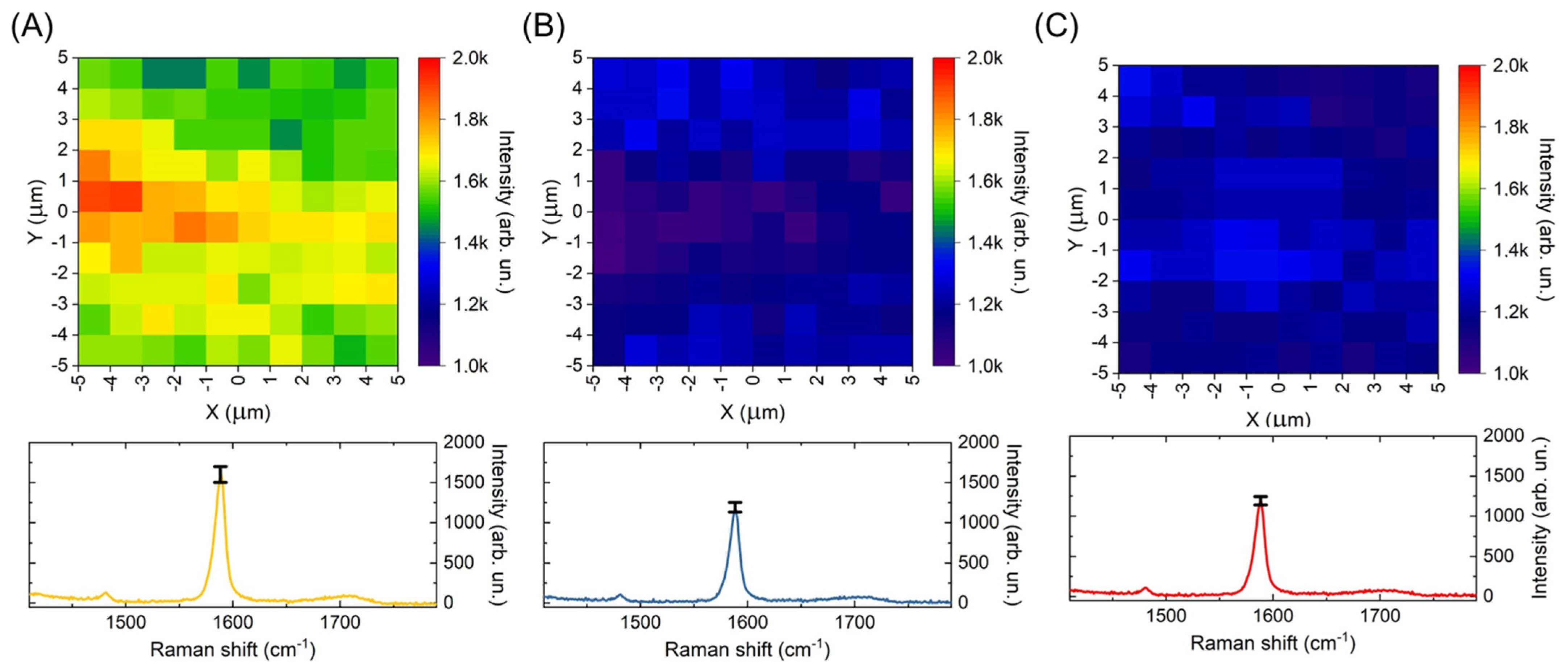
3. Experimental Results
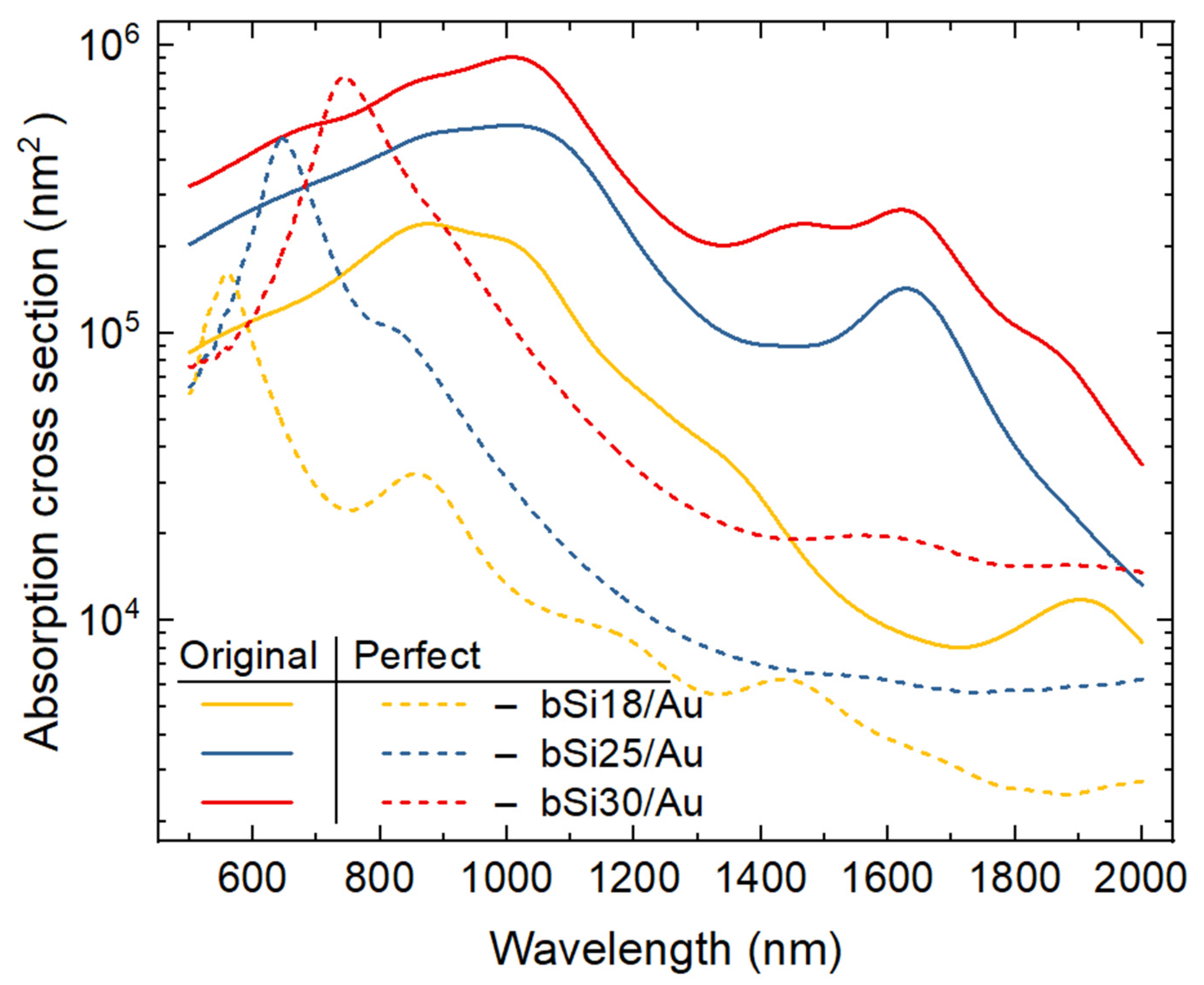
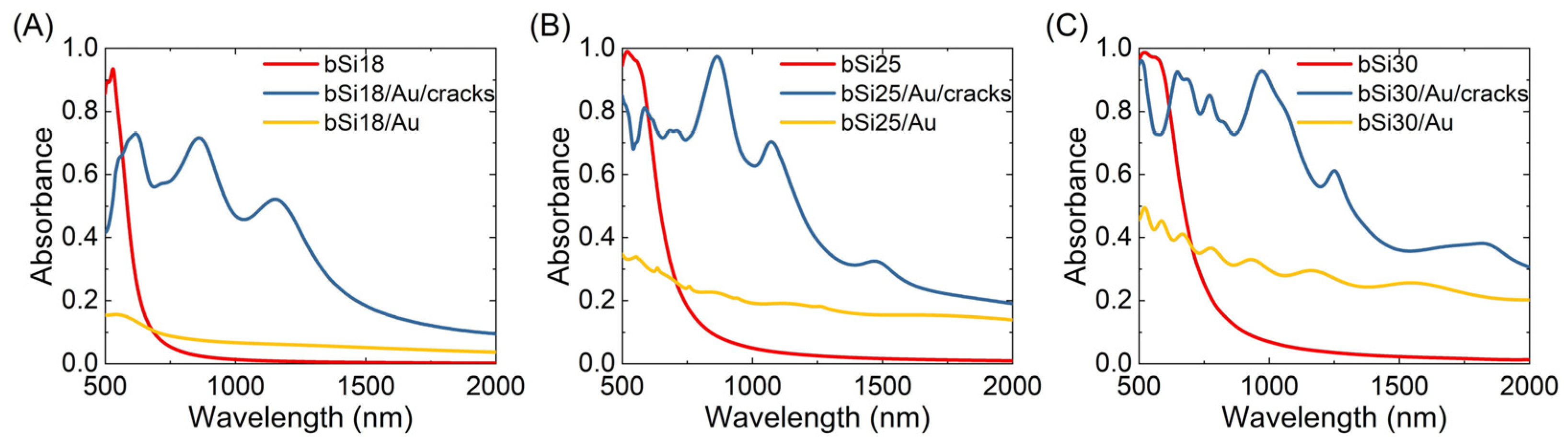
4. Numerical Simulation
5. Discussion
6. Conclusions
Author Contributions
Funding
Institutional Review Board Statement
Informed Consent Statement
Data Availability Statement
Acknowledgments
Conflicts of Interest
References
- Lv, J.; Zhang, T.; Zhang, P.; Zhao, Y.; Li, S. Review Application of Nanostructured Black Silicon. Nanoscale Res. Lett. 2018, 13, 110. [Google Scholar] [CrossRef] [PubMed]
- Yuan, H.C.; Yost, V.E.; Page, M.R.; Stradins, P.; Meier, D.L.; Branz, H.M. Efficient Black Silicon Solar Cell with a Density-Graded Nanoporous Surface: Optical Properties, Performance Limitations, and Design Rules. Appl. Phys. Lett. 2009, 95, 123501. [Google Scholar] [CrossRef]
- Lu, J.; Zhuang, W.; Yang, W.; Zhang, X.; Su, G.; Gong, X.; Yuan, J.; Sui, J.; Zhou, Y.; Zhang, G.; et al. Enhanced Absorption in the Wide Wavelength Range: Black Silicon Decorated with Few-Layer PtS2. J. Phys. Chem. C 2021, 125, 27335–27343. [Google Scholar] [CrossRef]
- Sarkar, S.; Elsayed, A.A.; Nefzaoui, E.; Drevillon, J.; Basset, P.; Marty, F.; Anwar, M.; Yu, Y.; Zhao, J.; Yuan, X.; et al. NIR and MIR Absorption of Ultra-Black Silicon (UBS). Application to High Emissivity, All-Silicon, Light Source. In Proceedings of the IEEE International Conference on Micro Electro Mechanical Systems (MEMS), Virtual, 25–29 January 2019; Institute of Electrical and Electronics Engineers Inc.: Piscataway, NJ, USA, 2019; Volume 2019, pp. 860–862. [Google Scholar]
- Zhang, P.; Li, S.; Liu, C.; Wei, X.; Wu, Z.; Jiang, Y.; Chen, Z. Near-Infrared Optical Absorption Enhanced in Black Silicon via Ag Nanoparticle-Induced Localized Surface Plasmon. Nanoscale Res. Lett. 2014, 9, 519. [Google Scholar] [CrossRef] [PubMed] [Green Version]
- Fan, Z.; Cui, D.; Zhang, Z.; Zhao, Z.; Chen, H.; Fan, Y.; Li, P.; Zhang, Z.; Xue, C.; Yan, S. Recent Progress of Black Silicon: From Fabrications to Applications. Nanomaterials 2021, 11, 41. [Google Scholar] [CrossRef] [PubMed]
- Wu, C.; Crouch, C.H.; Zhao, L.; Carey, J.E.; Younkin, R.; Levinson, J.A.; Mazur, E.; Farrell, R.M.; Gothoskar, P.; Karger, A. Near-Unity below-Band-Gap Absorption by Microstructured Silicon. Appl. Phys. Lett. 2001, 78, 1850–1852. [Google Scholar] [CrossRef]
- Wen, Z.; Shi, H.; Yue, S.; Li, M.; Zhang, Z.; Wang, R.; Song, Q.; Xu, Z.; Zhang, Z.; Hou, Y. Large-Scale Black Silicon Induced by Femtosecond Laser Assisted With Laser Cleaning. Front. Phys. 2022, 10, 235. [Google Scholar] [CrossRef]
- Zhong, H.; Ilyas, N.; Song, Y.; Li, W.; Jiang, Y. Enhanced Near-Infrared Absorber: Two-Step Fabricated Structured Black Silicon and Its Device Application. Nanoscale Res. Lett. 2018, 13, 316. [Google Scholar] [CrossRef]
- Chai, J.Y.H.; Wong, B.T.; Juodkazis, S. Black-Silicon-Assisted Photovoltaic Cells for Better Conversion Efficiencies: A Review on Recent Research and Development Efforts. Mater. Today Energy 2020, 18, 100539. [Google Scholar] [CrossRef]
- Ali, M.; Zhou, F.; Chen, K.; Kotzur, C.; Xiao, C.; Bourgeois, L.; Zhang, X.; MacFarlane, D.R. Nanostructured Photoelectrochemical Solar Cell for Nitrogen Reduction Using Plasmon-Enhanced Black Silicon. Nat. Commun. 2016, 7, 11335. [Google Scholar] [CrossRef] [Green Version]
- Oh, K.; Joanny, L.; Gouttefangeas, F.; Fabre, B.; Dorcet, V.; Lassalle-Kaiser, B.; Vacher, A.; Mériadec, C.; Ababou-Girard, S.; Loget, G. Black Silicon Photoanodes Entirely Prepared with Abundant Materials by Low-Cost Wet Methods. ACS Appl. Energy Mater. 2019, 2, 1006–1010. [Google Scholar] [CrossRef]
- Jian, J.X.; Liao, J.X.; Zhou, M.H.; Yao, M.M.; Chen, Y.J.; Liang, X.W.; Liu, C.P.; Tong, Q.X. Enhanced Photoelectrochemical Water Splitting of Black Silicon Photoanode with PH-Dependent Copper-Bipyridine Catalysts. Chem.—A Eur. J. 2022, 28, e202201520. [Google Scholar] [CrossRef] [PubMed]
- Bogue, R. Novel Infrared Detectors Based on Black Silicon. Sens. Rev. 2010, 30, 59–62. [Google Scholar] [CrossRef]
- Hu, F.; Dai, X.-Y.; Zhou, Z.-Q.; Kong, X.-Y.; Sun, S.-L.; Zhang, R.-J.; Wang, S.-Y.; Lu, M.; Sun, J. Black Silicon Schottky Photodetector in Sub-Bandgap near-Infrared Regime. Opt. Express 2019, 27, 3161. [Google Scholar] [CrossRef] [PubMed]
- Bodelón, G.; Montes-García, V.; Pérez-Juste, J.; Pastoriza-Santos, I. Surface-Enhanced Raman Scattering Spectroscopy for Label-Free Analysis of P. aeruginosa Quorum Sensing. Front. Cell Infect. Microbiol. 2018, 8, 143. [Google Scholar] [CrossRef] [PubMed]
- Pérez-Jiménez, A.I.; Lyu, D.; Lu, Z.; Liu, G.; Ren, B. Surface-Enhanced Raman Spectroscopy: Benefits, Trade-Offs and Future Developments. Chem. Sci. 2020, 11, 4563–4577. [Google Scholar] [CrossRef] [Green Version]
- Wang, J.; Lin, W.; Cao, E.; Xu, X.; Liang, W.; Zhang, X. Surface Plasmon Resonance Sensors on Raman and Fluorescence Spectroscopy. Sensors 2017, 17, 2719. [Google Scholar] [CrossRef] [Green Version]
- Tzeng, Y.; Lin, B.Y. Silver SERS Adenine Sensors with a Very Low Detection Limit. Biosensors 2020, 10, 53. [Google Scholar] [CrossRef]
- Costas, C.; López-Puente, V.; Bodelón, G.; González-Bello, C.; Pérez-Juste, J.; Pastoriza-Santos, I.; Liz-Marzán, L.M. Using Surface Enhanced Raman Scattering to Analyze the Interactions of Protein Receptors with Bacterial Quorum Sensing Modulators. ACS Nano 2015, 9, 5567–5576. [Google Scholar] [CrossRef]
- Morton, S.M.; Jensen, L. Understanding the Molecule-Surface Chemical Coupling in SERS. J. Am. Chem. Soc. 2009, 131, 4090–4098. [Google Scholar] [CrossRef]
- Kneipp, J. SERS for Sensing and Imaging in Live Cells. In Principles and Clinical Diagnostic Applications of Surface-Enhanced Raman Spectroscopy; Elsevier: Amsterdam, The Netherlands, 2021; pp. 303–325. ISBN 9780128211212. [Google Scholar]
- Bernat, A.; Samiwala, M.; Albo, J.; Jiang, X.; Rao, Q. Challenges in SERS-Based Pesticide Detection and Plausible Solutions. J. Agric. Food Chem. 2019, 67, 12341–12347. [Google Scholar] [CrossRef]
- Wang, Y.; Li, P.; Lin, D.; Chen, J.; Zhang, Y.; Yang, L. Ethanol-Extraction SERS Strategy for Highly Sensitive Detection of Poisons in Oily Matrix. Spectrochim. Acta—Part A Mol. Biomol. Spectrosc. 2021, 259, 119883. [Google Scholar] [CrossRef] [PubMed]
- Mo, S.; Shao, X.; Chen, Y.; Cheng, Z. Increasing Entropy for Colloidal Stabilization. Sci. Rep. 2016, 6, 36836. [Google Scholar] [CrossRef] [Green Version]
- Shi, L.; Zhang, L.; Tian, Y. Rational Design of Surface-Enhanced Raman Scattering Substrate for Highly Reproducible Analysis. Anal. Sens. 2022, 2022, e202200064. [Google Scholar] [CrossRef]
- Khnykina, K.A.; Baranov, M.A.; Babaev, A.A.; Dubavik, A.Y.; Fedorov, A.V.; Baranov, A.V.; Bogdanov, K.V. Comparison Study of Surface-Enhanced Raman Spectroscopy Substrates. J. Phys. Conf. Ser. 2021, 1984, 12020. [Google Scholar] [CrossRef]
- Mikac, L.; Gotić, M.; Gebavi, H.; Ivanda, M. The Variety of Substrates for Surface-Enhanced Raman Spectroscopy. In Proceedings of the 2017 IEEE 7th International Conference on Nanomaterials: Applications & Properties, (NAP 2017), Odessa, Ukraine, 10–15 September 2017. [Google Scholar] [CrossRef]
- Guo, R.; Hakala, T.K.; Törmä, P. Geometry Dependence of Surface Lattice Resonances in Plasmonic Nanoparticle Arrays. Phys. Rev. B 2017, 95, 155423. [Google Scholar] [CrossRef] [Green Version]
- Juluri, B.K.; Zheng, Y.B.; Ahmed, D.; Jensen, L.; Huang, T.J. Effects of Geometry and Composition on Charge-Induced Plasmonic Shifts in Gold Nanoparticles. J. Phys. Chem. C 2008, 112, 7309–7317. [Google Scholar] [CrossRef]
- Du, C.; Yang, W.; Peng, S.; Shi, D. Optimal Geometry Parameter for Plasmonic Sensitivities of Individual Au Nanopoarticle Sensors. Phys. Chem. Chem. Phys. 2019, 21, 7654–7660. [Google Scholar] [CrossRef]
- Serpenguzel, A. Luminescence of Black Silicon. J. Nanophoton. 2008, 2, 021770. [Google Scholar] [CrossRef] [Green Version]
- Jansen, H.; de Boer, M.; Burger, J.; Legtenberg, R.; Elwenspoek, M. The Black Silicon Method II:The Effect of Mask Material and Loading on the Reactive Ion Etching of Deep Silicon Trenches. Microelectron. Eng. 1995, 27, 475–480. [Google Scholar] [CrossRef] [Green Version]
- Cui, Z. Nanofabrication: Principles, Capabilities and Limits, 2nd ed.; Springer International Publishing: Cham, Switzerland, 2017; ISBN 9783319393612. [Google Scholar]
- Lawrence, K.P.; Douki, T.; Sarkany, R.P.E.; Acker, S.; Herzog, B.; Young, A.R. The UV/Visible Radiation Boundary Region (385–405 Nm) Damages Skin Cells and Induces “Dark” Cyclobutane Pyrimidine Dimers in Human Skin in Vivo. Sci. Rep. 2018, 8, 12722. [Google Scholar] [CrossRef] [PubMed] [Green Version]
- Godley, B.F.; Shamsi, F.A.; Liang, F.Q.; Jarrett, S.G.; Davies, S.; Boulton, M. Blue Light Induces Mitochondrial DNA Damage and Free Radical Production in Epithelial Cells. J. Biol. Chem. 2005, 280, 21061–21066. [Google Scholar] [CrossRef] [PubMed] [Green Version]
- Yuan, X.; Song, Y.; Song, Y.; Xu, J.; Wu, Y.; Glidle, A.; Cusack, M.; Ijaz, U.Z.; Cooper, J.M.; Huang, W.E.; et al. Effect of Laser Irradiation on Cell Function and Its Implications in Raman Spectroscopy. Appl. Environ. Microbiol. 2018, 84, 8. [Google Scholar] [CrossRef] [Green Version]
- Laermer, F.; Urban, A. MEMS at Bosch—Si Plasma Etch Success Story, History, Applications, and Products. Plasma Process. Polym. 2019, 16, 1800207. [Google Scholar] [CrossRef]
- Blauw, M.A.; Zijlstra, T.; van der Drift, E. Balancing the Etching and Passivation in Time-Multiplexed Deep Dry Etching of Silicon. J. Vac. Sci. Technol. B Microelectron. Nanom. Struct. 2001, 19, 2930. [Google Scholar] [CrossRef]
- Labelle, C.B.; Opila, R.; Kornblit, A. Plasma Deposition of Fluorocarbon Thin Films from C-C4F8 Using Pulsed and Continuous Rf Excitation. J. Vac. Sci. Technol. A Vacuum Surfaces Film. 2005, 23, 190–196. [Google Scholar] [CrossRef]
- Fu, H.; Bao, H.; Zhang, H.; Zhao, Q.; Zhou, L.; Zhu, S.; Wei, Y.; Li, Y.; Cai, W. Quantitative Surface-Enhanced Raman Spectroscopy for Field Detections Based on Structurally Homogeneous Silver-Coated Silicon Nanocone Arrays. ACS Omega 2021, 6, 18928–18938. [Google Scholar] [CrossRef]
- Ho, C.H.; Lee, S. SERS and DFT Investigation of the Adsorption Behavior of 4-Mercaptobenzoic Acid on Silver Colloids. Colloids Surfaces A Physicochem. Eng. Asp. 2015, 474, 29–35. [Google Scholar] [CrossRef]
- Barriet, D.; Yam, C.M.; Shmakova, O.E.; Jamison, A.C.; Lee, T.R. 4-Mercaptophenylboronic Acid SAMs on Gold: Comparison with SAMs Derived from Thiophenol, 4-Mercaptophenol, and 4-Mercaptobenzoic Acid. Langmuir 2007, 23, 8866–8875. [Google Scholar] [CrossRef]
- Mhlanga, N.; Ntho, T.A. A Theoretical Study of 4-Mercaptobenzoic Acid Assembled on Ag for Surface-Enhanced Raman Scattering Applications. Mater. Today Commun. 2021, 26, 101698. [Google Scholar] [CrossRef]
- Golubewa, L.; Karpicz, R.; Matulaitiene, I.; Selskis, A.; Rutkauskas, D.; Pushkarchuk, A.; Khlopina, T.; Michels, D.; Lyakhov, D.; Kulahava, T.; et al. Surface-Enhanced Raman Spectroscopy of Organic Molecules and Living Cells with Gold-Plated Black Silicon. ACS Appl. Mater. Interfaces 2020, 12, 50971–50984. [Google Scholar] [CrossRef] [PubMed]
- Michota, A.; Bukowska, J. Surface-Enhanced Raman Scattering (SERS) of 4-Mercaptobenzoic Acid on Silver and Gold Substrates. J. Raman Spectrosc. 2003, 34, 21–25. [Google Scholar] [CrossRef]
- Klyuchnik, A.V.; Kurganov, S.Y.; Lozovik, Y.E. Plasmons at a Hole in a Screen. Phys. Solid State 2003, 45, 1793–1797. [Google Scholar] [CrossRef]
- Rytov, S.M.; Kravtsov, Y.A.; Tatarskii, V.I. Wave Propagation through Random Media, Principles of Statistical Radiophysics 4; Springer: Berlin/Heidelberg, Germany, 1978; ISBN 9783642726842. [Google Scholar]
- Schinke, C.; Christian Peest, P.; Schmidt, J.; Brendel, R.; Bothe, K.; Vogt, M.R.; Kröger, I.; Winter, S.; Schirmacher, A.; Lim, S.; et al. Uncertainty Analysis for the Coefficient of Band-to-Band Absorption of Crystalline Silicon. AIP Adv. 2015, 5, 067168. [Google Scholar] [CrossRef] [Green Version]
- Lin, Y.J.; Chu, Y.L. Effect of Reactive Ion Etching-Induced Defects on the Surface Band Bending of Heavily Mg-Doped p -Type GaN. J. Appl. Phys. 2005, 97, 104904. [Google Scholar] [CrossRef]
- Weigel, C.; Brokmann, U.; Hofmann, M.; Behrens, A.; Rädlein, E.; Hoffmann, M.; Strehle, S.; Sinzinger, S. Perspectives of Reactive Ion Etching of Silicate Glasses for Optical Microsystems. J. Opt. Microsystems 2021, 1, 040901. [Google Scholar] [CrossRef]
- Alhmoud, H.; Brodoceanu, D.; Elnathan, R.; Kraus, T.; Voelcker, N.H. A MACEing Silicon: Towards Single-Step Etching of Defined Porous Nanostructures for Biomedicine. Prog. Mater. Sci. 2021, 116, 100636. [Google Scholar] [CrossRef]
- Arafat, M.Y.; Islam, M.A.; Mahmood, A.W.B.; Abdullah, F.; Nur-E-Alam, M.; Kiong, T.S.; Amin, N. Fabrication of Black Silicon via Metal-Assisted Chemical Etching—A Review. Sustainability 2021, 13, 766. [Google Scholar] [CrossRef]
- Kim, H.J.; Kim, B.; Lee, D.; Lee, B.-H.; Cho, C. Fabrication of Surface-Enhanced Raman Scattering Substrate Using Black Silicon Layer Manufactured through Reactive Ion Etching. J. Sens. Sci. Technol. 2021, 30, 267–272. [Google Scholar] [CrossRef]
- Gervinskas, G.; Seniutinas, G.; Hartley, J.S.; Kandasamy, S.; Stoddart, P.R.; Fahim, N.F.; Juodkazis, S. Surface-Enhanced Raman Scattering Sensing on Black Silicon. Ann. Phys. 2013, 525, 907–914. [Google Scholar] [CrossRef]
- Deng, Y.L.; Juang, Y.J. Black Silicon SERS Substrate: Effect of Surface Morphology on SERS Detection and Application of Single Algal Cell Analysis. Biosens. Bioelectron. 2014, 53, 37–42. [Google Scholar] [CrossRef] [PubMed]
- Lin, B.W.; Tai, Y.H.; Lee, Y.C.; Xing, D.; Lin, H.C.; Yamahara, H.; Ho, Y.L.; Tabata, H.; Daiguji, H.; Delaunay, J.J. Aluminum-Black Silicon Plasmonic Nano-Eggs Structure for Deep-UV Surface-Enhanced Resonance Raman Spectroscopy. Appl. Phys. Lett. 2022, 120, 51102. [Google Scholar] [CrossRef]


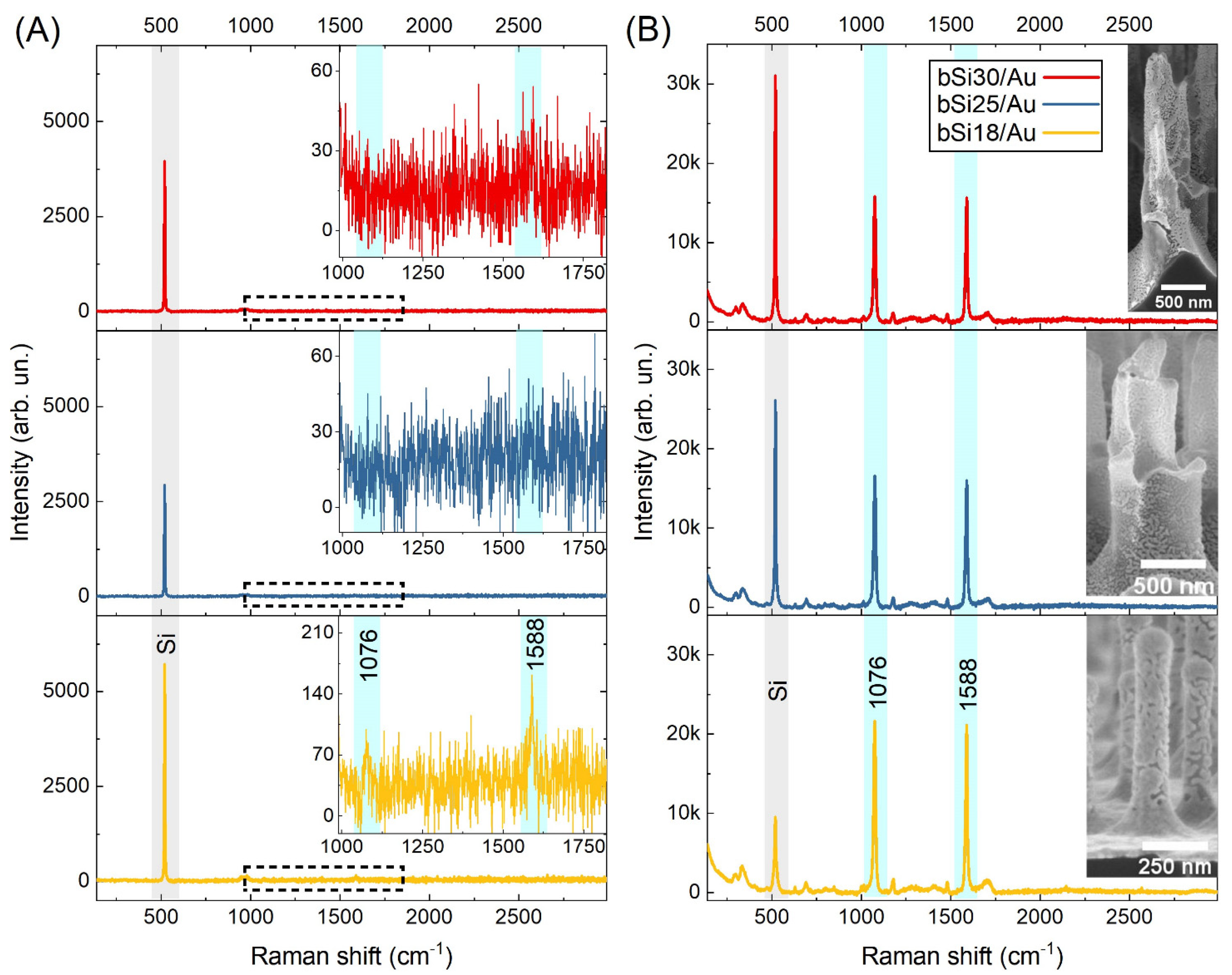
| Gasses | Flow (sccm) | Time (min) | RF (W) | ICP (W) | Pressure (mTorr) | DC Bias (V) | Temperature (°C) | He-Backside Cooling (sccm) | |
|---|---|---|---|---|---|---|---|---|---|
| Deposition | C4F8/SF6 | 40:1 | 1 | 20 | 295 | 20 | 100 | 20 | 5 |
| Etching | SF6/O2 | 10:9 | 18–30 | 30 | 0 | 30 | 100 | 20 | 10 |
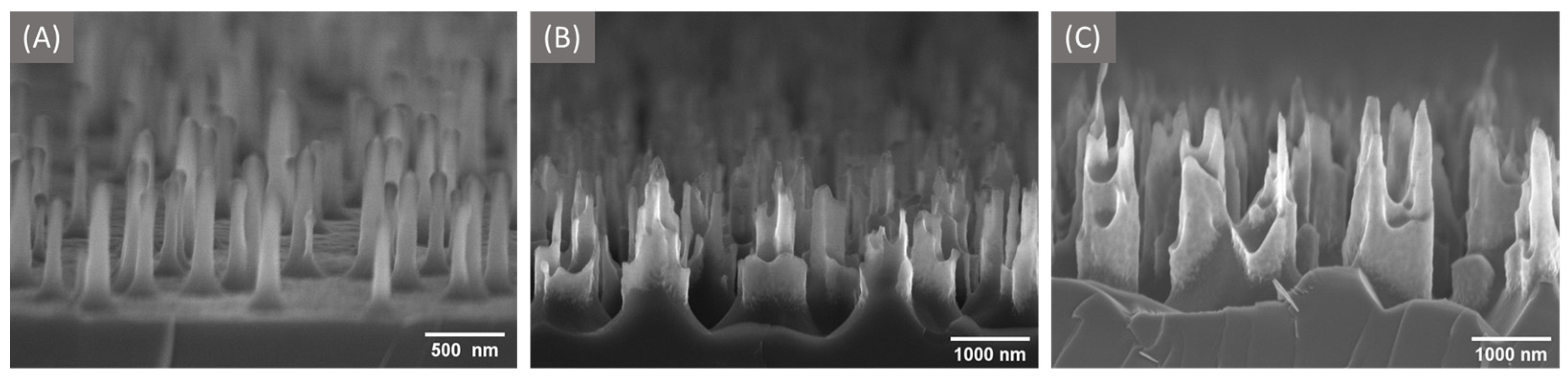
| Etching Time (min) | Height (nm) | Apex Thickness (nm) | Base Thickness (nm) | Pillars Density, pcs/μm2 |
|---|---|---|---|---|
 |  |  |  |  |
| 18 | 639 ± 126 | 112 ± 21 | 110 ± 32 | 4.33 |
| 25 | 1625 ± 298 | 125 ± 36 | 638 ± 155 | 1.12 |
| 30 | 2217 ± 433 | 144 ± 63 | 832 ± 377 | 0.56 |
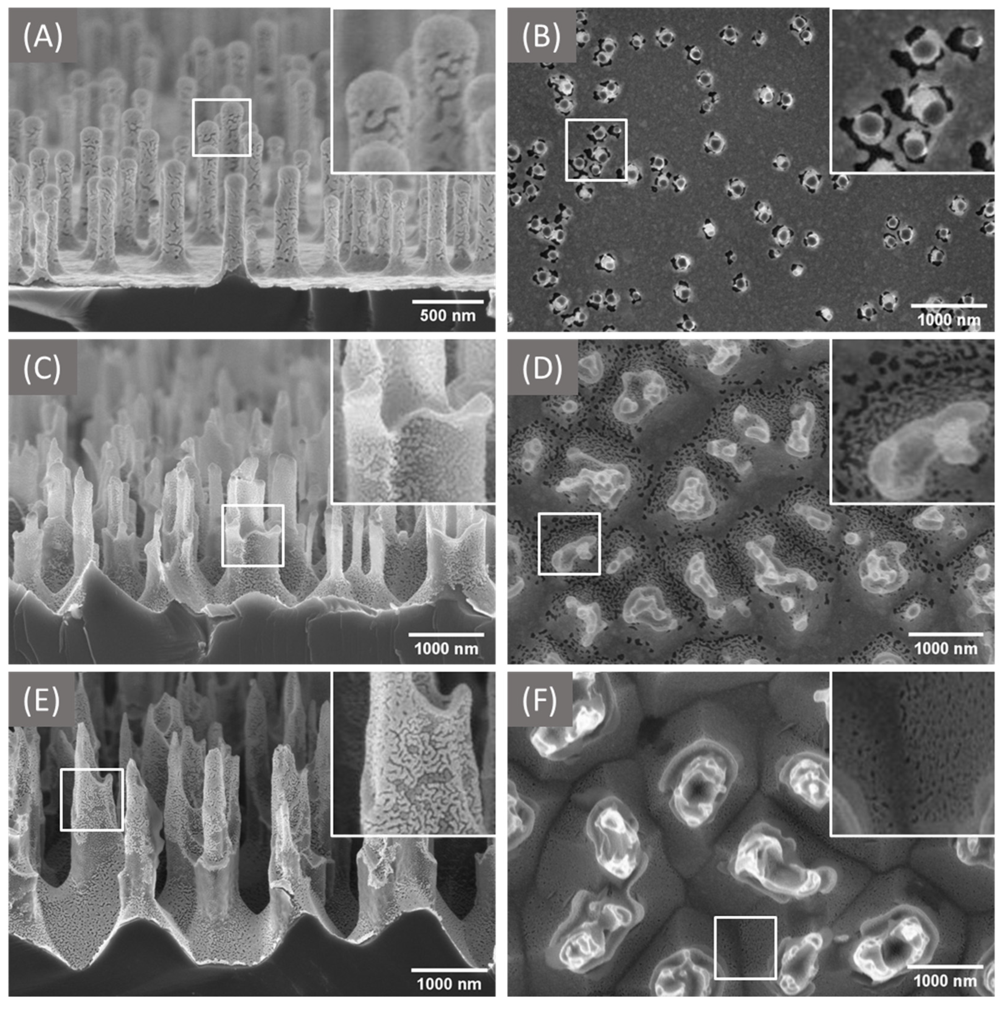
| Sample | Thickness of Au Layer (nm) | Type of Geometry | Area Uncovered with Au (%) |
|---|---|---|---|
| bSi18 | 25 ± 5 | Cylindrical pillars | 8.24 (98 μm2 was analyzed) |
| bSi25 | 14 ± 5 | Cylindrical pillars on stump | 9.03 (49 μm2 was analyzed) |
| bSi30 | 13 ± 4 | Spiked mountains | Difficult to analyze. Very mosaic structure |
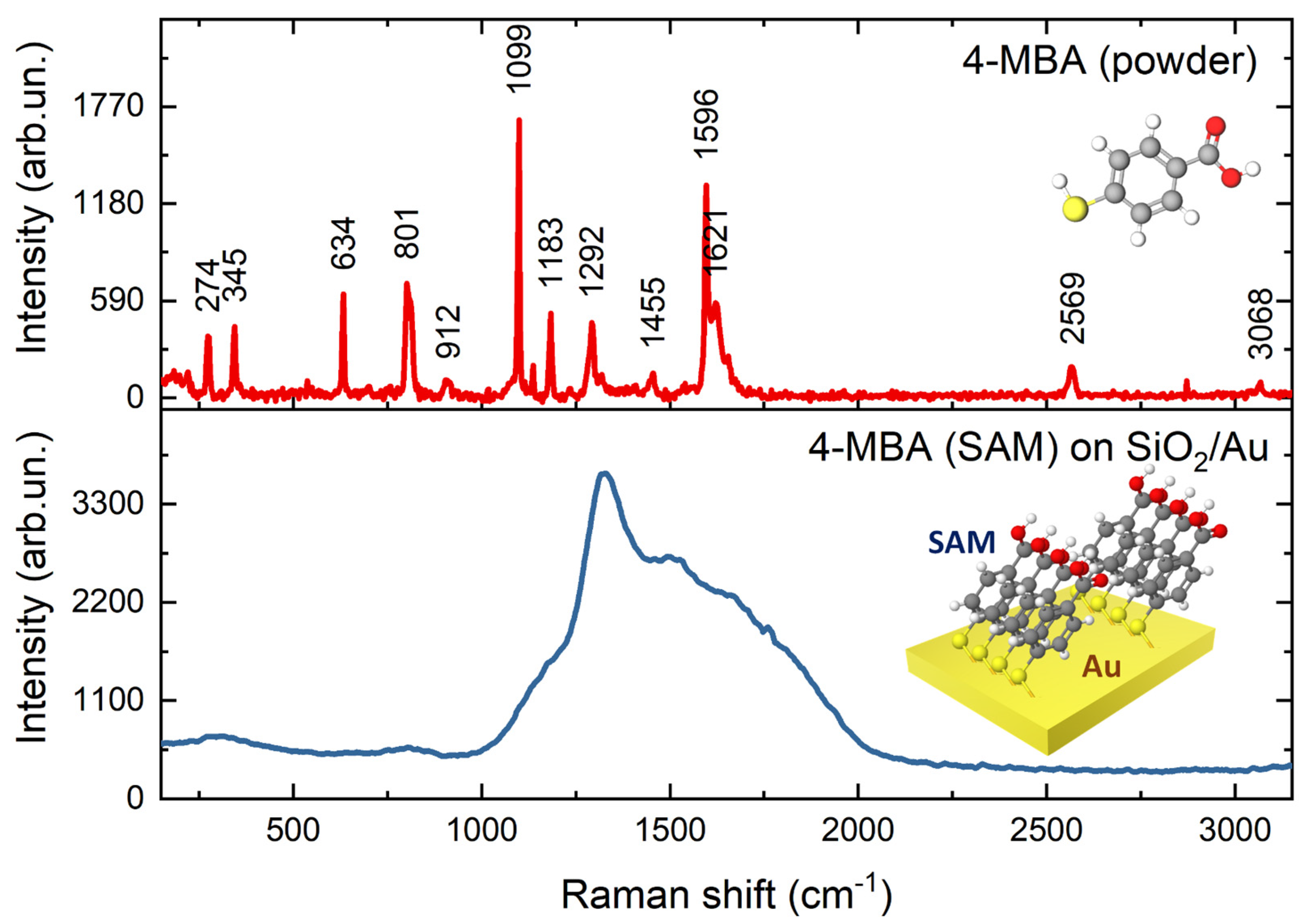
| 4-MBA Bulk (cm−1) | 4-MBA on bSi18/Au (cm−1) | Peak Assignments |
|---|---|---|
| 257 (w) | ν(Au-S) | |
| – | 520 (m) | Si (E2g mode) |
| 634 (m) # | 632 (w) | ν6b + δ(COOH) deformation |
| – | 691 (m) | γ(CH) out of plane |
| 801 (m) | – | ν10a in-plane aromatic ring breathing mode + -COH deformation |
| – | 848 (w) | β(COO–) |
| 912 (w) | – | β(SH) |
| 1099 (s) | 1076 (s) | ν12(a1) in-plane aromatic ring breathing mode + ν(CS) |
| 1183 (m) | 1182 (w) | ν9(a1) + δ(CH) deformation |
| 1292 (m) | – | ν3 |
| 1455 (w) | 1481 (w) | ν(CC) + γ(CH) |
| 1596 (s) | 1588 (s) | ν8a(a1) totally symmetric aromatic ring vibration |
| 1621 (m) | – | ν(C=O), ν(OC) + δ(HOC) |
| – | 1706 (m) | ν(C=O), COOH are hydrogen bonded [46] |
| 2569 (m) | – | ν(SH) stretching mode |
Disclaimer/Publisher’s Note: The statements, opinions and data contained in all publications are solely those of the individual author(s) and contributor(s) and not of MDPI and/or the editor(s). MDPI and/or the editor(s) disclaim responsibility for any injury to people or property resulting from any ideas, methods, instructions or products referred to in the content. |
© 2023 by the authors. Licensee MDPI, Basel, Switzerland. This article is an open access article distributed under the terms and conditions of the Creative Commons Attribution (CC BY) license (https://creativecommons.org/licenses/by/4.0/).
Share and Cite
Golubewa, L.; Rehman, H.; Padrez, Y.; Basharin, A.; Sumit, S.; Timoshchenko, I.; Karpicz, R.; Svirko, Y.; Kuzhir, P. Black Silicon: Breaking through the Everlasting Cost vs. Effectivity Trade-Off for SERS Substrates. Materials 2023, 16, 1948. https://0-doi-org.brum.beds.ac.uk/10.3390/ma16051948
Golubewa L, Rehman H, Padrez Y, Basharin A, Sumit S, Timoshchenko I, Karpicz R, Svirko Y, Kuzhir P. Black Silicon: Breaking through the Everlasting Cost vs. Effectivity Trade-Off for SERS Substrates. Materials. 2023; 16(5):1948. https://0-doi-org.brum.beds.ac.uk/10.3390/ma16051948
Chicago/Turabian StyleGolubewa, Lena, Hamza Rehman, Yaraslau Padrez, Alexey Basharin, Sumit Sumit, Igor Timoshchenko, Renata Karpicz, Yuri Svirko, and Polina Kuzhir. 2023. "Black Silicon: Breaking through the Everlasting Cost vs. Effectivity Trade-Off for SERS Substrates" Materials 16, no. 5: 1948. https://0-doi-org.brum.beds.ac.uk/10.3390/ma16051948