Article

NBTI-Aware Transient Fault Rate Analysis Method for Logic Circuit Based on Probability Voltage Transfer Characteristics

School of Electrical Engineering and Automation, Harbin Institute of Technology. No. 2 Yikuang Street, Harbin 150080, China
*
Author to whom correspondence should be addressed.
Submission received: 30 August 2015 / Revised: 5 November 2015 / Accepted: 14 January 2016 / Published: 18 January 2016

Abstract

:
The reliability of Very Large Scale Integration (VLSI) circuits has become increasingly susceptible to transient faults induced by environmental noise with the scaling of technology. Some commonly used fault tolerance strategies require statistical methods to accurately estimate the fault rate in different parts of the logic circuit, and Monte Carlo (MC) simulation is often applied to complete this task. However, the MC method suffers from impractical computation costs due to the size of the circuits. Furthermore, circuit aging effects, such as negative bias temperature instability (NBTI), will change the characteristics of the circuit during its lifetime, leading to a change in the circuit’s noise margin. This change will increase the complexity of transient fault rate estimation tasks. In this paper, an NBTI-aware statistical analysis method based on probability voltage transfer characteristics is proposed for combinational logic circuit. This method can acquire accurate fault rates using a discrete probability density function approximation process, thus resolving the computation cost problem of the MC method. The proposed method can also consider aging effects and analyze statistical changes in the fault rates. Experimental results demonstrate that, compared to the MC simulation, our method can achieve computation times that are two orders of magnitude shorter while maintaining an error rate less than 9%.

1. Introduction

Reliability issues have become a vital concern for Very Large Scale Integration (VLSI) design due to the continued scaling of VLSI technology and supply voltage. Among these reliability issues, transient faults caused by environmental effects, such as electrical noise, particle strikes, and electromagnetic coupling, are primary failure mechanisms [1]. In contrast to permanent faults, transient faults are temporary deviations of a circuit’s state from its correct or reference state. The occurrence of transient faults has certain random characteristics; therefore, statistical analysis methods are required to accurately analyze the effects of such faults on circuit performance [2]. In the past, environmental induced transient faults used to be a concern only in regarding memory because of the following two reasons. Firstly, the density of memory circuits is much higher than logic circuits, which makes the memory circuits contain the largest number and density of bits susceptible to transient fault. Secondly, the three masking factors affect the propagation of a transient fault through combinational circuit, which include logical masking, electrical masking and latching-window masking. However, in the last decade, supply voltage continues to diminish in value with current scaling trends, causing a decrease in the impact of these masking factors on logic circuits [3,4]. Furthermore, the high density and high speed of VLSI circuits also make the digital logic circuit more susceptible to transient faults induced by noise [5]. This trend will become more severe as the feature size of Complementary Metal Oxide Semiconductor (CMOS) devices approaches 22 nm, or even smaller scales, in the near future. Therefore, it is critical to model, analyze, and mitigate the impact of transient faults on VLSI circuits.
Existing transient fault mitigation methods can be generally classified into two categories: fault avoidance and fault correction methods. The first category generally exploits device fabrication processes to reduce the transient fault occurrence. These methods include the silicon-on-insulator process [6], the gate resizing strategy [7], and various other methods. The second category of methods functions at the circuit level or system level of abstraction to alleviate transient fault effects. Partial duplication [8], redundancy addition/removal [9], Delay Filtered Dual Interlocked storage Cell (DF-DICE) [10], and algorithmic noise tolerance (ANT) [11] are some typical methods used to address this issue. All of the above techniques suffer from area and energy overhead; therefore, to effectively and efficiently implement these mitigation methods, circuit designers require an accurate and fast transient fault modeling and analysis method to identify the part of a VLSI circuit that is most sensitive to transient faults. However, transient fault analysis has been difficult to implement due to the random characteristics of circuit design specifications, such as supply noise and input signal distribution. Therefore, statistical estimation methods are required to encapsulate all of these design conditions. Monte Carlo (MC) simulation is often applied to accomplish this task. However, the MC method suffers from an impractical computation cost due to the size of the circuits, and more efficient analysis methods are required.
In addition to transient faults, aging effects, such as hot carrier injection (HCI), time-dependent dielectric breakdown (TDDB), electro-migration (EM), and negative bias temperature instability (NBTI), are also major causes of VLSI reliability issues. Among these aging effects, NBTI is the main mechanism of circuit failure when the feature size approaches the 65 nm scale. NBTI occurs when positive-channel Metal Oxide Semiconductor (pMOS) transistors are negatively biased, which causes a shift in the threshold voltages (Vth) [12]. The reaction-diffusion (R-D) model is a widely used physical model for NBTI effect [13]. Yu Cao et al. developed a long-term Vth calculation formula based on the R-D model and noted that degradation caused by NBTI effect could cause a delay fault [14]. Moreover, NBTI may cause significant noise margin changes for digital circuits during the entire lifetime of circuits [15], and thus, transient fault rates are difficult to estimate. In [16], the authors proposed a methodology for modeling the transient fault propagation characteristics in the presence of process variation effect and obtained accurate estimation of transient fault rates for logic circuits. However, transient fault rate analysis under the influence of both environmental noise and aging effects has not yet been investigated in detail.
In this paper, we propose an NBTI-aware statistical analysis method to address transient fault rate estimation for combination logic circuit that considers both environmental noise and the NBTI effect. Our work is based on probability voltage transfer characteristics (PVTC) analysis and statistical modeling, which can provide accurate and efficient estimation of NBTI-aware transient fault rates, along with available statistical static timing analysis tools (SSTA) [17]. It should be noted that by introducing high-k/metal gate transistors in sub-45-nm technology, the PBTI effect becomes comparable to the NBTI effect [18]. Since the degradation effect of PBTI is similar to that of NBTI, the proposed approach can be easily extended to consider the PBTI effect as well.
The remainder of the paper is organized as follows. In Section 2, the principle of PVTC method is described. The procedure for performing PVTC analysis for single- and multi-gate circuits is presented. The NBTI-aware transient fault rate estimation is also introduced. Verification of the effectiveness of the proposed method by comparing the transient fault rate estimation results between the PVTC method and MC simulation is presented in Section 3. Moreover, the NBTI effect on changes in circuit characteristics and transient fault rates are also discussed. Conclusions are presented in Section 4.

2. Methodology

In recent years, noise-induced transient faults and circuit aging effects are two main mechanisms of VLSI circuit failure during its lifetime. These effects will change the timing and voltage levels of logic gates and can induce timing errors, voltage level distortion, or bit-flips when the influence accumulates to a certain degree. Most of the current transient fault analysis methods model the noise induced fault as a transient glitch and analyze the propagation characteristics of the glitch in the logic circuit. They focus on the timing errors of the circuit and apply the state-of-art statistical static timing analysis method to evaluate the timing effect. However, with respect to the voltage level, efficient analysis methods have not yet been studied in detail.
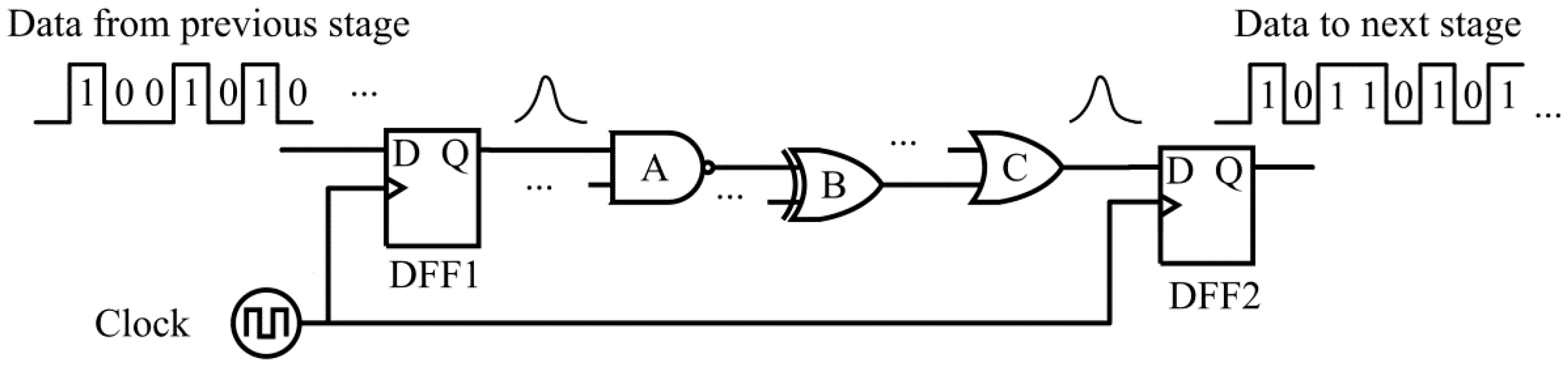
In VLSI design, sequential logic circuits are typically partitioned into pipeline stages separated by latches, as shown in Figure 1.
Figure 1. Pipeline stage structure of digital sequential circuits.
Algorithms 09 00009 g001
As shown in Figure 1, a noise-induced voltage transient (at the input port of NAND gate A) can become a voltage or timing fault only if it propagates to the end of one pipeline stage (at the input port of DFF2) and is stored in the latch. Thus, although hundreds of logic gates may exist in one pipeline stage, only the gates connected to the latch inputs are required to estimate the transient fault rates at the gates, and the computational complexity can be dramatically reduced. According to the characteristics of a CMOS logic circuit, the probability that a logic state is stored in the latch depends on the voltage level at the data input of that latch during the sampling time window. Because the noise-induced voltage transient arrives at the input of the latch at any point in the clock cycle with an equal probability, a high occurrence probability for the voltage transient will result in a high probability that the wrong logic state is captured by the latch. Therefore, the statistical analysis method proposed in this paper is applied to estimate the probability density function (pdf) of the voltage level at the end of one pipeline stage in the presence of noise effects. In a digital system, considering the low-pass characteristics of the logic gates and the central limit theorem, the effects of noise can be generally modeled as variations following a normal distribution in terms of the supply voltage and input signal of the pipeline stages, and MC simulation is commonly used to analyze these effects on circuit performance. However, the computational cost of MC is extremely high due to the complexity of the circuit. Some improved MC methods have effectively decreased the computational costs for transient fault rate analysis [19,
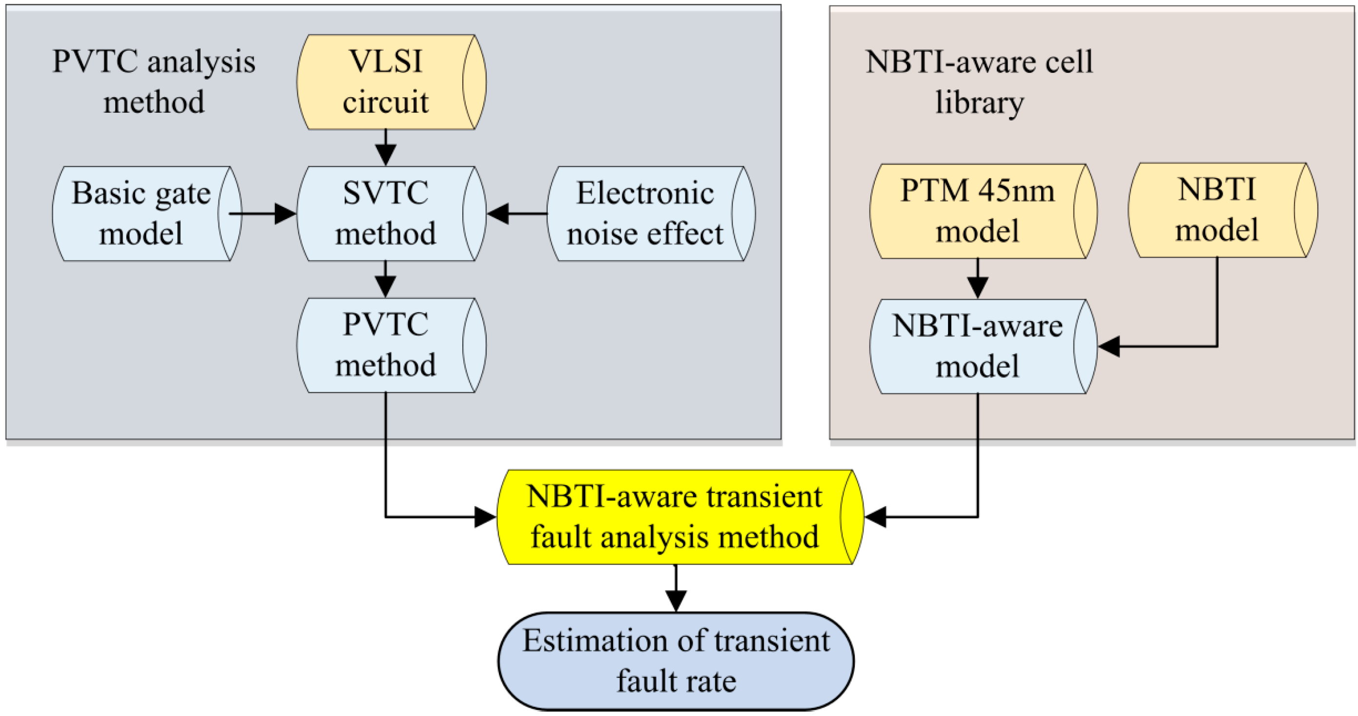
20] and have shortened the MC computation time. However, these methods do not consider the effects of some potential circuit characteristic changes in the analysis framework, such as aging effects, which undermine the accuracy of the analysis results during the lifetime of the circuit. Thus, in this paper, we propose a new NBTI-aware statistical analysis method to acquire accurate transient fault rates for different parts of the circuit to resolve the high computational cost problem of MC method. The design flow of the proposed method is shown in Figure 2.
As shown in Figure 2, when the random effects of circuit characteristics are not considered, the input and output relationship of VLSI circuits can be determined by the conventional static voltage transfer characteristics (SVTC) method. However, the input signal and supply voltage of the logic circuits are random variables instead of static values due to the effects of environmental noise. Therefore, the SVTC method is not sufficient to accurately calculate the output of logic circuits, and a statistical analysis method based on probability voltage transfer characteristics (PVTC) is proposed. Moreover, our method can also consider the effect of NBTI aging on circuit characteristics and analyze statistical changes in transient faults under NBTI effect such that the transient fault rates for different parts of VLSI circuits can be estimated accurately.
Figure 2. NBTI-aware transient fault rate analysis framework based on the PVTC method.
Algorithms 09 00009 g002

2.1. PVTC-Based Analysis for Single Logic Gates

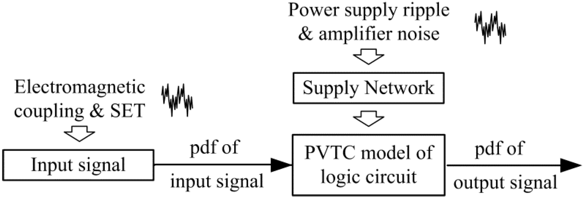
In VLSI design, a combinational circuit is composed of basic logic gate cells; thus, the transient fault analysis method begins with a single logic cell. In this paper, to describe the random characteristics of noise-induced effects, we apply a voltage level probability density function (pdf) to describe the input signal and supply and propose a PVTC method to establish the relationship between the input and output voltage pdf distributions of the logic gates. The basic scheme of the PVTC modeling method for logic gates is shown in Figure 3.
Figure 3. Diagram of the PVTC modeling method.
Algorithms 09 00009 g003
As shown in Figure 3, the function relationship between the voltage level of the input signal and output signal can be acquired by the PVTC model. Figure 4 provides an illustration of the procedure for establishing the PVTC model for an inverter gate.
Figure 4a presents an SVTC curve for an inverter gate by SPICE DC analysis, and the pdf of the input signal can be modelled as a random variable following a normal distribution due to the environmental noise effects, as shown in Figure 4c. Figure 4a,c show that the probability of the input signal falling into the shaded area [Vin1, Vin2] is equal to the probability of the output signal falling into the shaded area [Vout1, Vout2], and this relationship can be expressed as
P ( V o u t 2 < V o u t V o u t 1 ) = P ( V i n 1 V i n < V i n 2 )
However, Figure 4b illustrates that in the practical construction of an SVTC curve, instead of a continuous curve, only a series of discrete points can be acquired because of the actual characteristics of DC analysis. Therefore, the corresponding output signal point Vo for any input signal point Vi may not be found exactly in the discrete SVTC curve, which is necessary for the probability calculation in Equation (1). Thus, a discrete pdf approximation process must be used to implement the calculation. First, the input range of the signal is divided into a sequence of equal-length intervals by DC analysis, and the length of each interval is dVin, which can be set in the analysis process. We assume that, for each point (Vin,i, Vout,i) in the SVTC curve (e.g., point D in Figure 4b), input signals falling into area [Vin,idVin/2,Vin,i + dVin/2] or the corresponding output signal of area [VA,VC] all have the same voltage Vout,i. Furthermore, the approximation error can be tolerated because the division interval of dVin is small. Then, the probability of the output voltage level being equal to Vout,i can be calculated as
P ( V o u t , i ) = V A V C p ( V i n ) d V i n
Figure 4. Principle of the PVTC method for an inverter gate. (a) SVTC curve for an inverter gate; (b) Calculation of output signal’s pdf; (c) Voltage pdf for input signal Vin; (d) Division of Vin’s pdf.
Algorithms 09 00009 g004
Subsequently, to calculate the probability of the output signal falling into area [Vout2,Vout1], we search for all points (Vin,i,Vout,i) having an output signal belonging to this area in the SVTC curve. All of the P(Vout,i) of these points are then accumulated, and the probability of the output signal falling into the given area can be acquired. In the pdf calculation process, the gap between Vout1 and Vout2 is set to a small interval dVout; therefore, the pdf of area p(Vout) can be estimated as
p ( V o u t ) d V o u t P ( V o u t 2 < V o u t V o u t 1 ) i P ( V o u t , i ) i p ( V i n , i ) d V i n
where (Vin,i, Vout,i) is the ith point on the SVTC curve with Vout2 < Vout,iVout1.
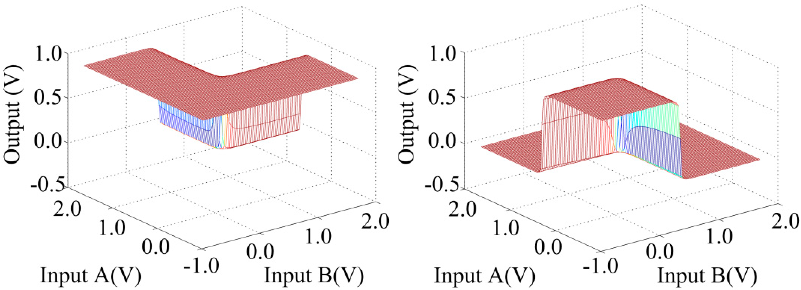
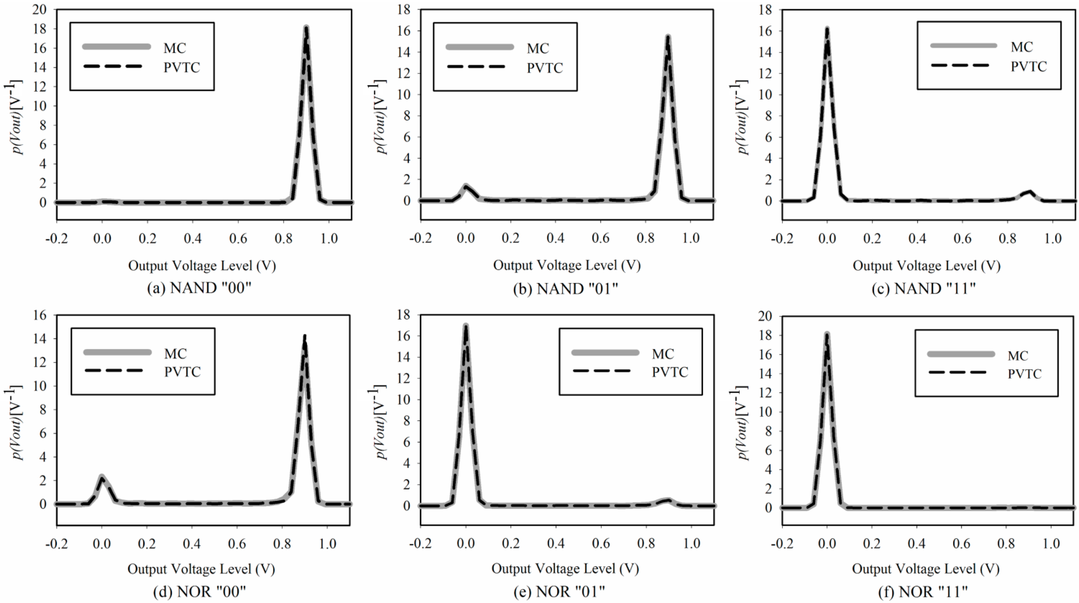
PVTC analysis for gates with multiple input ports, such as NAND and NOR gates, can be modelled by a similar method. However, the SVTC curves for these gates are extended to three-dimensional curves (two or more input axes and one output axis), as shown in Figure 5.
Figure 5. Three-dimensional SVTC curves for multi-input gates. (a) SVTC of NAND gate; (b) SVTC of NOR gate.
Algorithms 09 00009 g005
In Figure 5, the x- and y-axes are the two input voltage levels, and the z-axis is the output voltage level. The pdf calculation for the output signal Vout is expressed as
p ( V o u t ) d V o u t P ( V o u t 2 < V o u t V o u t 1 ) i P ( V o u t , i ) i p ( V i n 1 , i ) d V i n 1 p ( V i n 2 , i ) d V i n 2
where (Vin1,i,Vin2,i,Vout,i) is the ith point on the three-dimensional SVTC curve with Vout2 < Vout,iVout1.
Accurate analysis of transient fault occurrence probabilities, or transient fault rates for different parts of circuits, is an important step for the effective implementation of transient fault mitigation techniques. Therefore, after acquiring the pdf of a circuit’s output ports, we can calculate the transient fault rate Perror for these ports. Figure 6 presents an illustration of the transient fault rate calculation for an inverter gate whose normal state is input “one” and output “zero”.
Figure 6. Transient fault rate calculation for an inverter with input “one”.
Algorithms 09 00009 g006
As shown in Figure 6, the two shaded areas in the figure are the probability of logic “0” and logic “1”. Then, Perror can be calculated according to Equation (5):
P e r r o r = P ( V o u t > V h i g h , min | V n o m = 0 ) = i p ( V o u t , i ) d V o u t
where Vhigh,min is the voltage threshold for logic “one”, Vnom is the expected correct voltage for the output signal, and p(Vout,i) is the estimated pdf of the points whose Vout,i is greater than Vhigh,min.

2.2. PVTC-Based Analysis for Multi-Gate Circuits

Transient fault analysis for single gates is clearly not sufficient. Digital logic circuits typically consist of hundreds of gates, and there is complex logic dependency between them, meaning that the pdf of the output of one gate is the pdf of the input of another gate. The pdf calculation result for the single gate obtained in Section 2.1 is a series of discrete points, which is not suitable for estimating the pdf for gates in the next stage. Therefore, some approximation procedures are required, and the Riemann sum p(Vin)dVin is applied to substitute for the integration ∫p(Vin)dVin in Equations (3) and (4). We then obtain the modified pdf calculation equation for single- and multi-input gates in Equations (6) and (7), respectively.
p ( V o u t ) d V o u t P ( V o u t 2 < V o u t V o u t 1 ) i p ( V i n , i ) d V i n
p ( V o u t ) d V o u t P ( V o u t 2 < V o u t < V o u t 1 ) i P ( V o u t , i ) i p ( V i n 1 , i ) d V i n 1 p ( V i n 2 , i ) d V i n 2
where (Vin,i,Vout,i) or (Vin1,i,Vin2,i,Vout,i) is the ith point on the SVTC curve with Vout2 < Vout,iVout1.
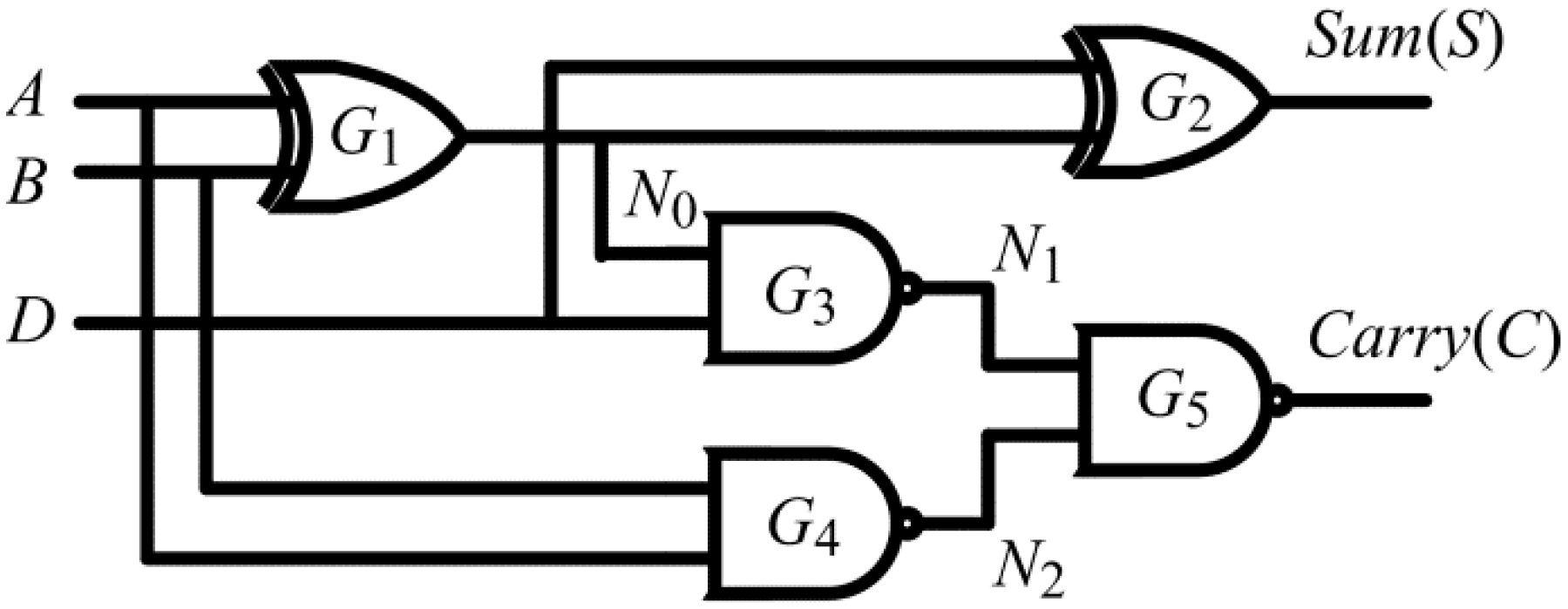
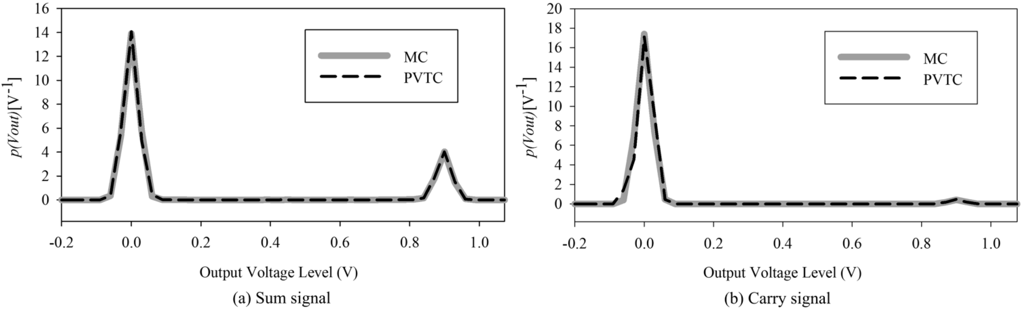
However, the functional complexity of actual circuits usually results in re-convergent fan-out characteristics, which causes different input ports of one gate to be interdependent. The full adder in Figure 7 is an illustration of re-convergent fan-out characteristics.
Figure 7. Illustration of the re-convergent fan-out characteristics in a multi-gate circuit.
Algorithms 09 00009 g007
As shown in Figure 7, the output signal C for the full adder circuit is determined by the inputs of gate G5, N1 and N2. Port N1 is the output of NAND gate G3 and is determined by the root input signals A, B, and D. Port N2 is the output of NAND gate G4 and is determined by A and B. Therefore, the two input ports of gate G5 are not independent. Thus, in the pdf calculation of the output signal C of G5, the correlation between input ports N1 and N2 must be considered, as the calculation may otherwise lead to inaccurate results. To solve this problem, the pdf calculation formula Equation (7) is adapted by considering the dependence between N1 and N2 because these two signals are both related to root inputs A and B. The total probability formula Equation (8) is applied to estimate the pdf of the output signal C, which considers conditional probability of input ports N1 and N2 of gate G5 on the root input signals VA and VB.
p ( V C ) d V C P ( V C 2 < V C V C 1 ) i P ( V C , i ) V A , j , V B , j i p ( V N 1 , i | V A = V A , j , V B = V B , j ) d V N 1 p ( V N 2 , i | V A = V A , j , V B = V B , j ) d V N 2
In Equation (8), point (VN1,i,VN2,i,VC,i) is the ith point on the SVTC curve of gate G5 with VC2 < VC,iVC1. (VA,j,VB,j) is each input voltage pair of the discrete three-dimensional SVTC curve acquired by SPICE DC analysis, as shown in Figure 5. The conditional probability p(VN2,i|VA = VA,j,VB = VB,j) can be calculated directly because VN2 is determined by VA and VB only, whereas VN1 is determined by D and N0, and the pdf estimate of the conditional probability p(VN0,i|VA = VA,j,VB = VB,j) can be acquired by a similar method to that of N2. The conditional probability p(VN1,i|VA = VA,j,VB = VB,j) can then be found by calculating the pdf estimate of gate G3, and the final result of the pdf calculation for gate G5’s output C can be determined. The pdf estimation for other logic circuits can also be obtained by a similar method.

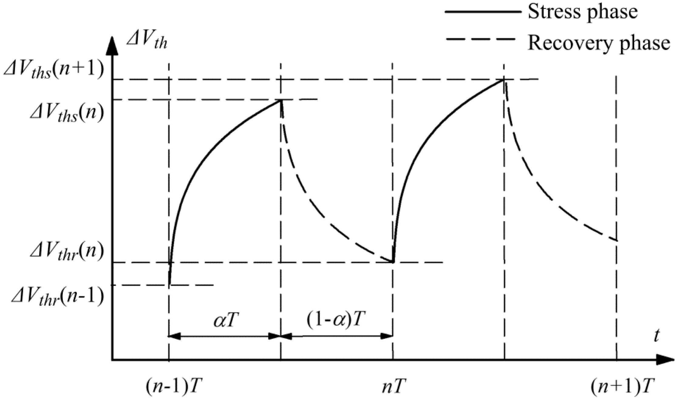
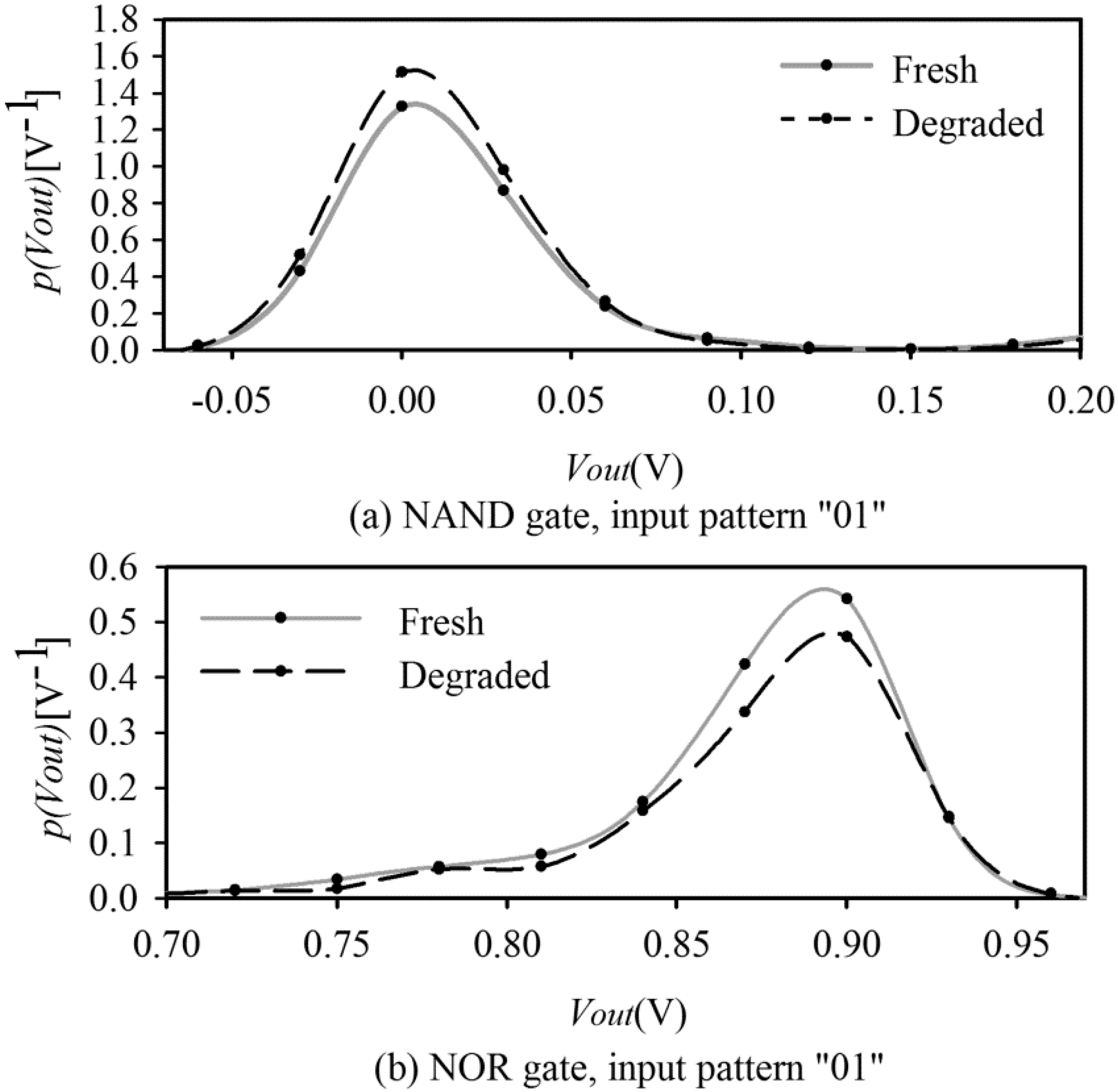
2.3. NBTI Effect and Its Impact on the PVTC Method

At present, the NBTI effect is the dominant aging mechanism for VLSI circuits; this effect occurs when pMOS transistors are negatively biased, which causes a shift in the threshold voltages (Vth) and in turn causes changes in circuit characteristics during its lifetime. Grasser et al. [21] noted that in small-sized devices in CMOS logic circuits, the threshold voltage change induced by the NBTI effect is dominated by stochastic charging/discharging events of individual oxide defects; therefore, each device shows a different degradation curve. Clearly, this type of NBTI model will greatly complicate the analysis process. Because our aim was to estimate the transient fault rate that considers both environmental noise and the NBTI effect and provide a design basis for transient fault mitigation techniques, in this paper, pMOS transistors are assumed to suffer the same degree of degradation during the lifetime of the circuits, and the R-D model is applied to analyze the NBTI effect. According to the R-D model, the Vth degradation of pMOS transistors caused by NBTI has two phases: the stress phase and the recovery phase. The magnitude of Vth increases during the stress phase (i.e., Vgs = −Vdd), whereas the magnitude of Vth partially decreases towards its initial value during the recovery phase (i.e., Vgs = 0); however, recovery can only partially alleviate the effect of NBTI. The threshold voltage change during stress and recovery cycles is illustrated in Figure 8.
Figure 8. Threshold voltage change during stress and recovery cycles.
Algorithms 09 00009 g008
Therefore, the magnitude of Vth degradation is strongly dependent on the duty cycle (α) of the input signal, which reflects the fraction of time that the pMOS transistor spent in the stress state in one clock period. In this paper, we apply the long-term prediction model proposed in [14] to calculate the Vth degradation effect as follows
| Δ V t h | = ( K v 2 T c l k α / ( 1 β t 1 / 2 n ) ) 2 n
where β t = 1 ( 2 ξ 1 t e + ξ 2 C ( 1 α ) T c l k ) / ( 2 t o x + C t ) , and 
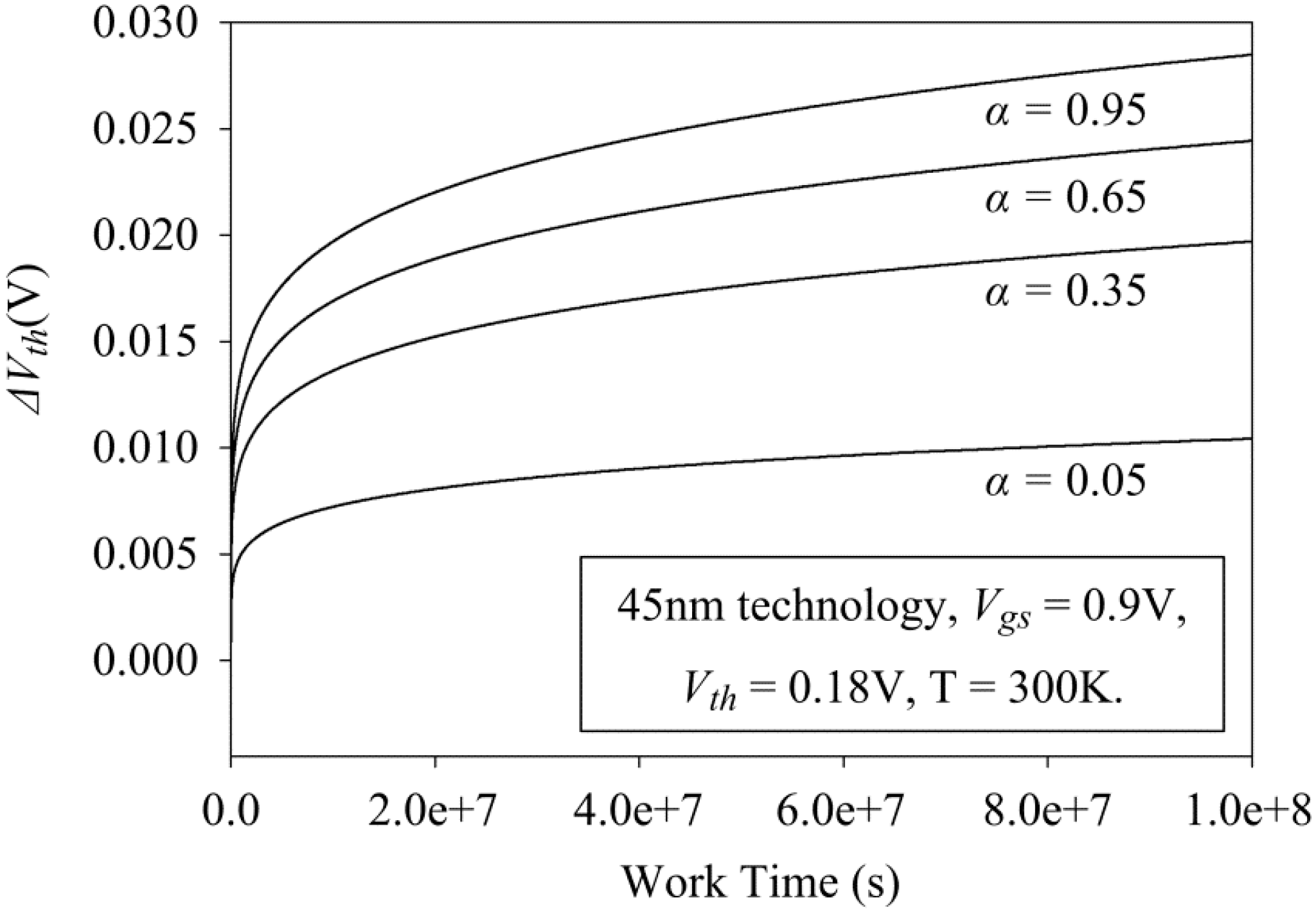
Tclk is the clock period. According to the formula Equation (9), we simulate the NBTI effect of a pMOS transistor using the PTM 45 nm model [22] in HSPICE. The increase in Vth after working 108 s (approximately 3 years) is presented in Figure 9. The duty cycle (α) of the NBTI effect is set from 0.05 to 0.95, with a step of 0.3.
Figure 9. Change of Vth vs. work time under different duty cycles of an input signal.
Algorithms 09 00009 g009
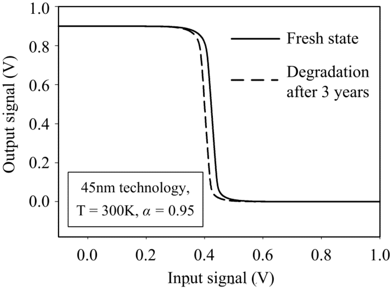
The change in the SVTC curve for an inverter gate caused by the Vth increase is shown in Figure 10; this change, in turn, affects the occurrence probability of transient faults. Therefore, to acquire accurate transient fault rate estimations during the lifetime of circuits, changes in circuit characteristics caused by NBTI effect should be considered in the PVTC analysis framework.
Figure 10. Changes in the SVTC of an inverter in the fresh and degraded states.
Algorithms 09 00009 g010

3. Results and Discussion

3.1. Experimental Setup

We divide the noise sources into two categories to simulate the actual working conditions of circuits in a noise-filled environment: input noise and supply noise. Considering the low-pass characteristics of logic gates and the central limit theorem, these two types of noise are modelled as random variables following a normal distribution. The input noise represents external noise effects, such as single event transient and electromagnetic coupling, and the amplitudes of these noises are relatively large. Additionally, as the probability of error in actual circuits is very small, an extremely long time is required for the MC simulation to obtain the overall transient fault rate. Therefore, the standard deviation of the noise on the input signal is set to 300 mV such that the MC simulation can be implemented within a reasonable time to verify the effectiveness of the PVTC method. Supply noises, which represent noise effects inside the VLSI circuit system, such as power supply ripple and amplifier noise of the linear regulator, are also considered; the amplitudes of these noises are relatively small, and thus, their standard variation is set to 20 mV. The supply noise and the input noise are assumed to be independent. In our experiment, dVout and dVin are set to the same value to simplify the experiment, and dVout and dVin are set to the small value of 30 mV to guarantee accuracy.
The predictive technology model (PTM) [22] for 45 nm general-purpose pMOS and nMOS transistors is exploited to evaluate the PVTC method, and the power supply of the logic circuit is set to 0.9 V. In NBTI effect simulation, the duty cycle for the pMOS transistor is set to 0.95, as in [23] by the MDS method, temperature T is set to 300 K. In the transient error rate calculation, Vhigh,min in Equation (5) is set to 0.7 V, which represents logic “1”, whereas Vlow,max is set to 0.2 V, which represents logic “0”. The number of iterations for MC simulation is set to 10,000. The above configuration is the same for all of the experiments.

3.2. The PVTC Method for the Logic Circuit

First, we build the voltage level pdf at the output of the basic logic gate cell based on the PVTC method and MC simulation. Figure 11 presents the voltage pdf curve for the NAND gate with an input of “11” by these two methods.
As shown in Figure 11, the majority of the output is distributed around “0”, which is a correct result for the NAND gate. However, due to the influence of noise effects, a minority of the output voltage level is distributed around “1”. We can also find that the pdf estimation results by two methods are highly similar. Furthermore, Figure 12a–f presents the level pdf for the NAND gate and NOR gate with different input combinations. In Figure 12, the dashed lines are the pdf curve estimated by the PVTC method, and the solid lines are the pdf curve acquired by the MC method. Figure 12 illustrates that the voltage pdf estimation curves obtained by the two methods are all highly similar for different input combinations, thus verifying the effectiveness of the proposed method. Moreover, Figure 12a,c illustrate that the probability of occurrence for a transient fault is less when the input is “00” compared to when the input is “11” for the NAND gate due to the logical masking effect of combinational circuits. We can observe similar phenomena based on the results of the NOR gate.
Figure 11. The pdf estimation of the output of the NAND gate with input “1, 1”.
Algorithms 09 00009 g011
To fully investigate the effectiveness of the PVTC method, a multi-gate circuit is also tested. Here, the full adder in Figure 7 is selected, which is a frequently used structure in pipeline stages. Because the result of N2 is determined by inputs A and B and node N1 is also related to inputs A and B, there is a correlation between N1 and N2. Conditional probability should be considered. Figure 13a,b present the level pdf curve for the sum signal and carry signal of the full adder circuit, respectively. To provide a brief illustration of the result, only the result with an input of “000” is listed. We also implemented experiments using other input combinations and obtained similar results.
Figure 12. The level pdf for the NAND and NOR gates with different inputs. (a) NAND “00”; (b) NAND “01”; (c) NAND “11”; (d) NOR “00”; (e) NOR “01”; (f) NOR “11”.
Algorithms 09 00009 g012
Figure 13. PVTC analysis for a full-adder circuit. (a) Sum signal; (b) Carry signal.
Algorithms 09 00009 g013
A comparison of the results of the transient fault rate and the runtime between the PVTC and MC simulations is shown in Table 1. We also calculate the error between the results obtained by the PVTC and MC simulations, which is defined as follows: (PVTC-MC)/MC. The experiments are conducted on a PC with a 3.30 GHz Intel Core i3-2120, 3GB RAM, and the 32-bit Windows 8 operating system. The PVTC method is implemented in a Matlab R2011b simulation environment, and the MC simulations are implemented in an HSPICE C-2009.9 environment. Table 1 shows that the error between the two methods is less than 9%, which is sufficient for the transient fault mitigation design requirement. Moreover, the computational cost of the PVTC method is far less than that of the MC simulation, as the PVTC method is approximately two orders of magnitude faster than the MC method. As the transient fault rate when the input is “01” is the same as the rate when the input is “10” for the NAND gate, we only list the transient fault rate when the input is “01” for the NAND and NOR gates in Table 1.
Table 1. Comparison of the results of the probability voltage transfer characteristics (PVTC) method and Monte Carlo (MC) simulation.
Logic CircuitInputTransient Fault Rate (%)Error (%)Runtime (s)
MCPVTCMCPVTC
NAND Gate000.810.888.62200.41
018.989.111.4
117.527.46−0.8
NOR Gate0015.4714.80−4.32300.39
014.774.41−7.5
110.230.21−8.7
FA Sum00022.7122.880.74521.0
FA Carry0002.572.55−0.84521.8

3.3. NBTI-Aware PVTC Method Analysis

To explore how the NBTI effect can affect the transient fault rate of digital circuits, we add the NBTI model to the PVTC analysis framework. Table 2 presents the transient fault estimation results for NAND and NOR gates and the full adder circuit when the circuit is in a fresh state and after three years of NBTI degradation. We also calculate the change rate before and after degradation, which is defined as follows: (Degraded-Fresh)/Fresh.
As shown in Table 2, the NBTI effect causes a significant transient fault rate change for different parts of the VLSI circuit during its lifetime. Moreover, as the feature size, supply voltage and threshold voltage continue to decrease, this change will become more severe in the future. These results also illustrate that the transient fault rate will increase for certain gates with a certain input pattern, but the opposite situation is observed for other gates with the same input pattern combination (Table 2). A detailed illustration of the fault rate change for the NAND and NOR gates with the same input pattern, in a fresh state and degraded state, respectively, is provided in Figure 14.
Table 2. Comparison of the transient fault rate before and after negative bias temperature instability (NBTI) degradation.
Logic CircuitInputTransient Fault Rate (%)Change Rate (%)
FreshDegraded
NAND Gate000.881.03+17.1
019.1110.11+11.0
117.466.51−12.7
NOR Gate0014.8016.89+14.1
014.413.78−14.3
110.210.16−23.8
FA Sum00022.8825.11+9.8
FA Carry0002.553.22+26.3
As shown in Figure 14a, the gate will be more sensitive to transient faults after degradation when the input pattern of the NAND gate is “01”; in contrast, the same pattern “01” results in a transient fault rate decrease for the NOR gate, as shown in Figure 14b. This result is mainly due to the different functions of the logic gates. When the threshold voltage of the pMOS increases, an input of “0” will be more likely to be recognized as “1”; thus, the transient fault rate will be more likely to increase with an input of “00”, whereas the transient fault rate will be more likely to decrease with an input of “11” for both the NAND and NOR gates. If the input is “01”, the NOR gate is more likely to logically mask the error, whereas the NAND gate is not, which creates the different trends in the change rate. Thus, during the entire lifetime of a VLSI circuit, we can provide more accurate fault rate estimation results if NBTI effect is considered.
Figure 14. Transient fault rate change before and after degradation. (a) NAND gate, input pattern “01”; (b) NOR gate, input pattern “01”.
Algorithms 09 00009 g014

4. Conclusions

Transient faults and the NBTI aging effect are two main failure mechanisms for modern VLSI systems. In this paper, an NBTI-aware statistical analysis method is proposed to analyze the transient fault rates of combinational logic circuits induced by environmental noise. The new method is based on PVTC, which can acquire accurate fault rates using a discrete probability density function approximation method with a reasonable computational cost. Moreover, the proposed method also considers the NBTI effect on the estimation process of the transient fault rate and analyzes the impact of input combinations on the highest transient fault rate for different parts of the circuit. Experimental results at different levels of abstract circuit design have demonstrated the effectiveness of the proposed method. The NBTI-aware PVTC method can provide a design basis for different transient fault mitigation methods and improve long-term reliability during the lifetime of VLSI circuits.

Acknowledgments

This work was supported by the National Natural Science Foundation of China (No. 61201015, 61102036).

Author Contributions

Zhiming Yang conceived and designed the experiments; Yang Yu performed the experiments; Junbao Li analyzed the data; Zhiming Yang and Xiyuan Peng wrote the paper.

Conflicts of Interest

The authors declare no conflict of interest.

References

  1. Polian, I.; Hayes, J.P.; Reddy, S.M.; Becker, B. Modeling and mitigating transient errors in logic circuits. IEEE Trans. Dependable Secur. Comput. 2011, 8, 537–547. [Google Scholar] [CrossRef]
  2. Chang, A.C.C.; Huang, R.H.M.; Wen, C.H.P. Casser: A closed-form analysis framework for statistical soft error rate. IEEE Trans. Very Large Scale Integr. 2013, 21, 1837–1848. [Google Scholar] [CrossRef]
  3. Miskov-Zivanov, N.; Marculescu, D. Multiple transient faults in combinational and sequential circuits: A systematic approach. IEEE Trans. Comput. Aided Des. Integr. Circuits Syst. 2010, 29, 1614–1627. [Google Scholar] [CrossRef]
  4. Liu, X.; Zhang, Y.; Yuan, F.; Xu, Q. Layout-Aware Pseudo-Functional Testing for Critical Paths Considering Power Supply Noise Effects. In Proceedings of the Design, Automation and Test in Europe Conference and Exhibition, DATE 2010, Dresden, Germany, 8–12 March 2010; pp. 1432–1437.
  5. Ramanarayanan, R.; Degalahal, V.; Krishnan, R.; Kim, J.S.; Narayanan, V.; Xie, Y.; Irwin, M.J.; Unlu, K. Modeling soft errors at the device and logic levels for combinational circuits. IEEE Trans. Dependable Secur. Comput. 2009, 6, 202–216. [Google Scholar] [CrossRef]
  6. Zhou, Q.M.; Mohanram, K. Cost-Effective Radiation Hardening Technique for Combinational Logic. In Prorceedings of the 2004 IEEE/ACM International conference on Computer-aided design, San Jose, CA, USA, 7–11 November 2004; pp. 100–106.
  7. Zhou, Q.M.; Mohanram, K. Gate sizing to radiation harden combinational logic. IEEE Trans. Comput. Aided Des. Integr. Circuits Syst. 2006, 25, 155–166. [Google Scholar] [CrossRef]
  8. Mohanram, K.; Touba, N.A. Cost-Effective Approach for Reducing Soft Error Failure Rate in Logic Circuits. In Proceedings of the International Test Conference 2003, Charlotte, NC, USA, 30 September–2 October 2003; pp. 893–901.
  9. Kai-Chiang, W.; Marculescu, D. A low-cost, systematic methodology for soft error robustness of logic circuits. IEEE Trans. Very Large Scale Integr. Syst. 2013, 21, 367–379. [Google Scholar]
  10. Naseer, R.; Draper, J. DF-DICE: A Scalable Solution for Soft Error Tolerant Circuit Design. In Proceedings of the 2006 IEEE International Symposium on Circuits and Systems, Island of Kos, Greece, 21–24 May 2006; pp. 3890–3893.
  11. Shim, B.Y.; Sridhara, S.R.; Shanbhag, N.R. Reliable low-power digital signal processing via reduced precision redundancy. IEEE Trans. Very Large Scale Integr. 2004, 12, 497–510. [Google Scholar] [CrossRef]
  12. Wang, W.P.; Yang, S.Q.; Bhardwaj, S.; Vrudhula, S.; Liu, F.; Cao, Y. The impact of NBTI effect on combinational circuit: Modeling, simulation, and analysis. IEEE Trans. Very Large Scale Integr. 2010, 18, 173–183. [Google Scholar] [CrossRef]
  13. Huard, V.; Denais, M.; Parthasarathy, C. NBTI degradation: From physical mechanisms to modeling. Microelectron. Reliab. 2006, 46, 1–23. [Google Scholar] [CrossRef]
  14. Bhardwaj, S.; Wang, W.P.; Vattikonda, R.; Cao, Y.; Vrudhula, S. Predictive Modeling of the NBTI Effect for Reliable Design. In Proceedings of the Custom Integrated Circuits Conference, San Jose, CA, USA, 10–13 September 2006; pp. 189–192.
  15. Reddy, V.; Krishnan, A.T.; Marshall, A.; Rodriguez, J.; Natarajan, S.; Rost, T.; Krishnan, S. Impact of negative bias temperature instability on digital circuit reliability. Microelectron. Reliab. 2005, 45, 31–38. [Google Scholar] [CrossRef]
  16. Chopra, K.; Cheng, Z.; Blaauw, D.; Sylvester, D. Process Variability-Aware Transient Fault Modeling and Analysis. In Proceedings of the IEEE/ACM International Conference on Computer-Aided Design, 2008, ICCAD 2008, San Jose, CA, USA, 10–13 November 2008; pp. 685–690.
  17. Agarwal, A.; Chopra, K.; Blaauw, D.; Zolotov, V.; Soc, I.C. Circuit optimization using statistical static timing analysis. In Proceedings of the 42nd Design Automation Conference, Anaheim, CA, USA, 13–17 June 2005; pp. 321–324.
  18. Stathis, J.H.; Wang, M.; Zhao, K. Reliability of advanced high-k/metal-gate n-FET devices. Microelectron. Reliab. 2010, 50, 1199–1202. [Google Scholar] [CrossRef]
  19. Schleifer, J.; Coenen, T.; Noll, T.G. Statistical modeling of reliability in logic devices. Microelectron. Reliab. 2011, 51, 1469–1473. [Google Scholar] [CrossRef]
  20. Huang, H.M.; Wen, C.H.P. Fast-yet-accurate statistical soft-error-rate analysis considering full-spectrum charge collection. IEEE Des. Test 2013, 30, 77–86. [Google Scholar] [CrossRef]
  21. Grasser, T.; Kaczer, B.; Goes, W.; Reisinger, H.; Aichinger, T.; Hehenberger, P.; Wagner, P.J.; Schanovsky, F.; Franco, J.; Luque, M.T.; et al. The paradigm shift in understanding the bias temperature instability: From reaction-diffusion to switching oxide traps. IEEE Trans. Electron Devices 2011, 58, 3652–3666. [Google Scholar] [CrossRef]
  22. Zhao, W.; Cao, Y. New Generation of Predictive Technology Model for Sub-45 nm Design Exploration; IEEE Computer Soc: Los Alamitos, CA, USA, 2006; pp. 585–590. [Google Scholar]
  23. Agarwal, M.; Balakrishnan, V.; Bhuyan, A.; Kim, K.; Paul, B.C.; Wang, W.P.; Yang, B.; Cao, Y.; Mitra, S.; Society, I.C. Optimized Circuit Failure Prediction for Aging: Practicality and Promise. In Proceedings of the 2008 IEEE International Test Conference, Santa Clara, CA, USA, 28–30 October 2008; IEEE Computer Soc: Los Alamitos, CA, USA, 2008; pp. 656–665. [Google Scholar]

