Influence of Thermal Annealing on the PdAl/Au Metal Stack Ohmic Contacts to p-AlGaN


1
School of Electronics Engineering, Kyungpook National University, Daegu 41566, Korea
2
Advanced Material Research Center, Kumoh National Institute of Technology, Gumi 39177, Korea
*
Author to whom correspondence should be addressed.
Crystals 2020, 10(12), 1091; https://0-doi-org.brum.beds.ac.uk/10.3390/cryst10121091
Submission received: 5 October 2020
/
Revised: 24 November 2020
/
Accepted: 25 November 2020
/
Published: 28 November 2020
(This article belongs to the Special Issue Nano/Micro and Bio-Inspired Materials on Wide-Bandgap-Semiconductor-Based Optoelectronic/Power Devices)
Abstract
:In this study, a PdAl (20 nm)/Au (30 nm) metal stack scheme is used for forming low-ohmic-resistance contact on Mg-doped (1.5 × 1017 cm−3) p-type AlGaN at various annealing temperatures. Using a circular-transmission line model, the specific contact resistance (ρc) of PdAl/Au/p-AlGaN ohmic contact is determined via the current–voltage (I–V) characteristics. As-deposited contacts demonstrate non-linear behavior. However, the contact exhibits linear I–V characteristics with excellent ohmic contact of ρc = 1.74 × 10⁻⁴ Ωcm2, when annealed at 600 °C for 1 min in a N2 atmosphere. The Ga and Al vacancies created at the PdAl/Au and p-AlGaN interfaces, which act as acceptors to increase the hole concentration at the interface. The out-diffusion of Ga as well as in-diffusion of Pd and Au to form interfacial chemical reactions at the interface is observed by X-ray photoelectron spectroscopy (XPS) measurements. The phases of the Ga–Pd and Ga–Au phases are detected by X-ray diffraction (XRD) analysis. Morphological results show that the surface of the contact is reasonably smooth with the root-mean-square roughness of 2.89 nm despite annealing at 600 °C. Based on the above experimental considerations, PdAl/Au/p-AlGaN contact annealed at 600 °C is a suitable p-ohmic contact for the development of high-performance electronic devices.
1. Introduction
The development of high-performance ohmic metal contacts on n/p-type AlGaN and n/p-type InGaN is increasing their potential for use in high-quality electro-optic devices, such as laser diodes, light-emitting diodes, and high-power/frequency high-electron-mobility transistors (HEMTs) [1,2,3,4]. Various metallization schemes, such as the use of Ti/Al, Ti/Ta/Al, Ta/Ti/Al, and Ti/Al/(Ti, Ni, Mo, Pd, and Pt)/Au, were used as ohmic contacts for n-type AlGaN [5,6,7,8]. For the aforementioned metallization schemes, the specific contact resistivity (ρc) obtained is low, ranging from ~10−5 to 10−8 Ω cm2 [5,6,7,8], making them highly applicable to electronic devices, such as HEMTs and metal-semiconductor field-effect transistors MESFETs.
In particular, solid-state ultraviolet (UV) emitters for general lighting application require AlGaN layers with relatively high Al composition and hence the formation of ohmic contact on these layers, especially on p-AlGaN layer, is much more difficult. Two main problems arise regarding the construction of good ohmic contact; (i) it is very difficult to grow a highly Mg-doped p-AlGaN, (ii) metal with work function higher than p-AlGaN is rare. Due to these obstacles, only a few studies have been conducted so far [9,10,11,12,13,14]. For example, Blank et al. [9] found a potential barrier of approximately 2.3 V at the Pd/p-Al0.06Ga0.94N contact after the thermal treatment. Jun et al. [10] applied a Pd/Au (35/100 nm) metal scheme on p-type Al0.15Ga0.85N with an acceptor concentration of 6 × 1016 cm−3. They observed a linear current–voltage (I–V) curve after thermal annealing at 700 °C for 2 min in a N2 atmosphere. Kim et al. [11] demonstrated a low-resistance ohmic contact with a specific contact resistivity of 3.1 × 10⁻⁴ Ω cm2 on the moderately doped p-AlGaN:Mg (1.5 × 1017 cm−3) applying a Pt/Pd/Au (5/5/10 nm) metal scheme and annealing at 600 °C for 1 min in a N2 atmosphere. Chary et al. [12] investigated the Au/Ni layer to achieve an ohmic contact on p-type GaN and AlGaN, which is annealed at 500 °C for 10 min in a N2 (90%) and O2 (10%) atmosphere, and found the lowest specific contact resistance (ρc) of ~9.2 × 10⁻⁶ and 1.8 × 10⁻⁴ Ω cm2 for p-GaN and p-AlGaN, respectively.
In the present study, we applied a PdAl/Au metallization contact to p-type AlGaN to obtain reliable, low-ohmic-resistance contacts. A PdAl metallic alloy was used as the first layer because it has a heat of formation (ΔH = –92 kJ/g atom) as well as low chemical reactivity with AlGaN. In addition, Au was used as a top coating film to protect the metal stack scheme from the ambient during annealing process. The main focus of this study was to investigate a reliable, low-ohmic-resistance contact of PdAl/Au metallic stacks on p-type AlGaN, which was characterized before and after annealing by using the rapid thermal process (RTP). The mixing of the metallic alloyed contacts with the diffusion of Ga, N, Pd, Al, and Au from the PdAl/Au metallic stacks and p-type Al0.15Ga0.85N was observed via X-ray photoelectron spectroscopy (XPS) depth profiles. The interface products were determined by an X-ray diffractometer (XRD), and the roughness of the contact’s surface was observed with a scanning probe microscopy (SPM) measurement.
2. Materials and Methods
The epitaxial structure studied in this work consisted of 1.5 μm-thick undoped GaN and 0.2 μm-thick Mg-doped Al0.15Ga0.85N layers with carrier concentration of ~1.5 × 1017 cm−3, which were sequentially grown on c-plane Al2O3 sapphire using a metal–organic chemical vapor deposition method. Prior to the metallization, the p-AlGaN films were ultrasonically cleaned with warm acetone, followed by isopropyl alcohol, for 5 min each. The films were then dipped into a buffer-oxide-etch solution for 10 min to remove the native surface oxides, and then dipped in deionized water. The patterns for the circular transmission line model (CTLM) were arranged on the p-AlGaN film with standard photolithography. A PdAl (20 nm)/Au (30 nm) metallic scheme comprising a PdAl metal alloy as the first layer (90 wt% of Pd/10 wt% of Al) and Au as the second layer were deposited on the p-AlGaN surface using the electron beam evaporation method followed by rapid thermal annealing (RTA) for 1 min at 400 °C, 500 °C, 600 °C, and 700 °C for each sample in a N2 atmosphere. I–V curves were measured with a Keithley 4200 semiconductor parameter analyzer. XPS (Thermo Fisher Scientific Inc.) was performed to observe the in-/out-diffusion of the metal stacks and p-AlGaN before and after annealing using Al Kα radiation (1486.6 eV). We used the sputter with each rate ~5.34 nm/min for the characterization of atomic compositions of XPS depth profiles. XRD (PANalytical) with Cu Kα energy was used to illustrate the interface phases between the stack metals and p-AlGaN films. The morphological roughness of the contacts was analyzed using scanning probe microscopy (NX-20 SPM Controller, Park Systems) before and after annealing.
3. Results and Discussion
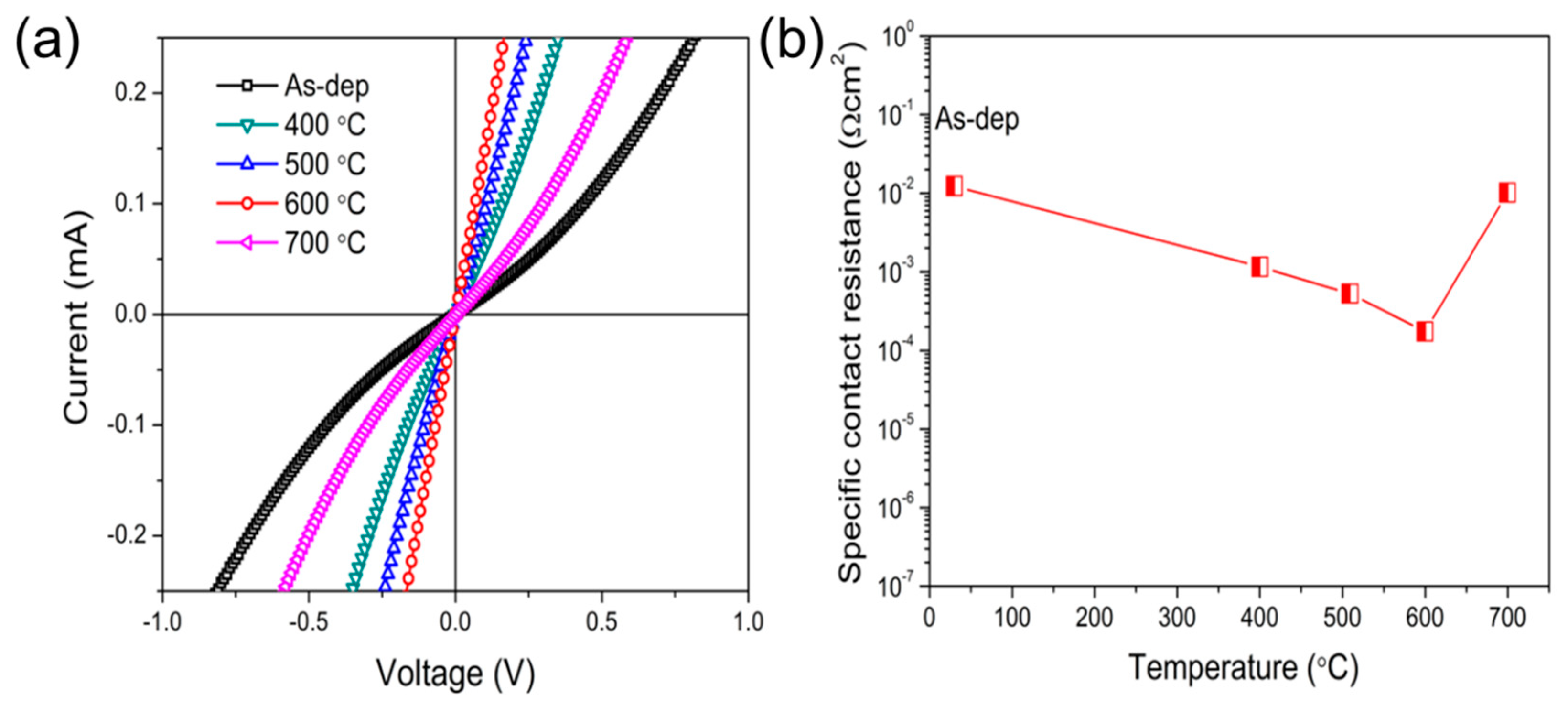
Figure 1a displays the I–V curves of the PdAl/Au metallization contacts on p-AlGaN annealed at various temperatures, using CTLM with a spacing of 5 μm. A non-linear I–V behavior was observed in the as-deposited PdAl/Au/p-AlGaN ohmic contact, but the curve became linear when the contact was annealed at 400 °C and the slope of the curve increased as the annealing temperature increased up to 600 °C. When the temperature increased to 700 °C, however, the contact was apparently deteriorated showing non-linear I-V characteristics again. As shown in Figure 1b, the estimated ρc is 1.23 × 10⁻² Ω cm2 for the as-deposited film. For the samples annealed at 400, 500, 600, and 700 °C, the ρc values are 1.16 × 10⁻³, 5.27 × 10⁻⁴, 1.74 × 10⁻⁴, and 1.01 × 10⁻² Ωcm2, respectively. The lowest ρc is achieved when the contact is annealed at 600 °C, meaning that the best annealing temperature is 600 °C for PdAl/Au metallic contacts on p-AlGaN. It is also noticed that the ρc of 1.74 × 10⁻⁴ Ω cm2 is the lowest value, even compared to those of various ohmic schemes obtained from other research groups as summarized in Table 1 [9,10,11,12,13,14]. The degradation of the contact annealed at 700 °C can be attributed to rough surface morphology at the ohmic contact, caused by the severe amalgamation between the PdAl/Au metal and p-AlGaN may be due to the instability of p-AlGaN crystal structure [15].
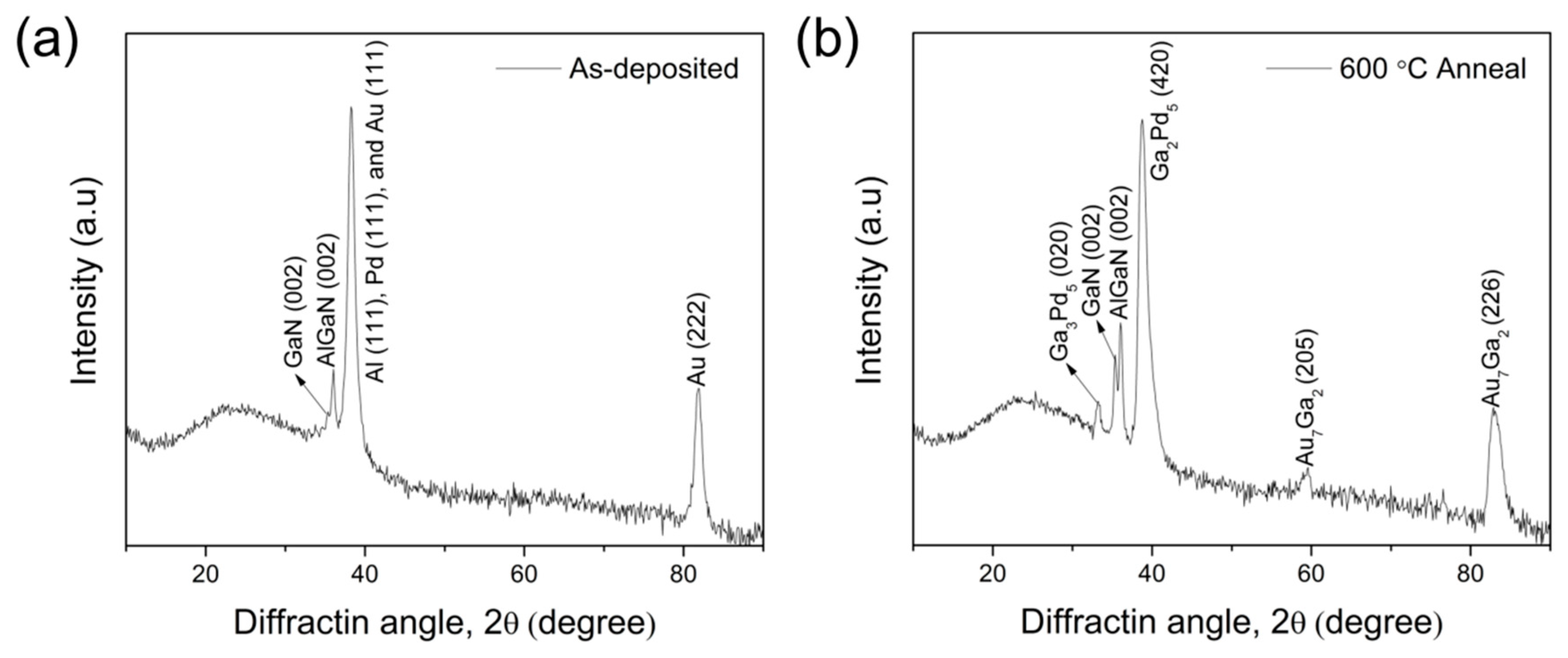
XRD examination was performed to study the interfacial phases formed between the PdAl/Au metal alloyed layers and GaN films before and after annealing at 600 °C. Figure 2a illustrates the XRD plot of the as-deposited contact. The diffraction plot reveals the distinctive substrate peaks of GaN (002) and AlGaN (002) were observed. In addition, superposition of peaks from pure metals Al (111), Pd (111) and Au (111) were observed at ~38.25°. Furthermore, a diffraction peak of Au (222) was observed at ~81.85°. After annealing at 600 °C (Figure 2b), additional interfacial peaks were identified compared to the as-deposited contacts. These interfacial peaks were identified as Ga3Pd5 (020), Ga2Pd5 (420), Au7Ga2 (205), and Au7Ga2 (226), which provide the Ga–Pd and Ga–Au metal-compound phases.
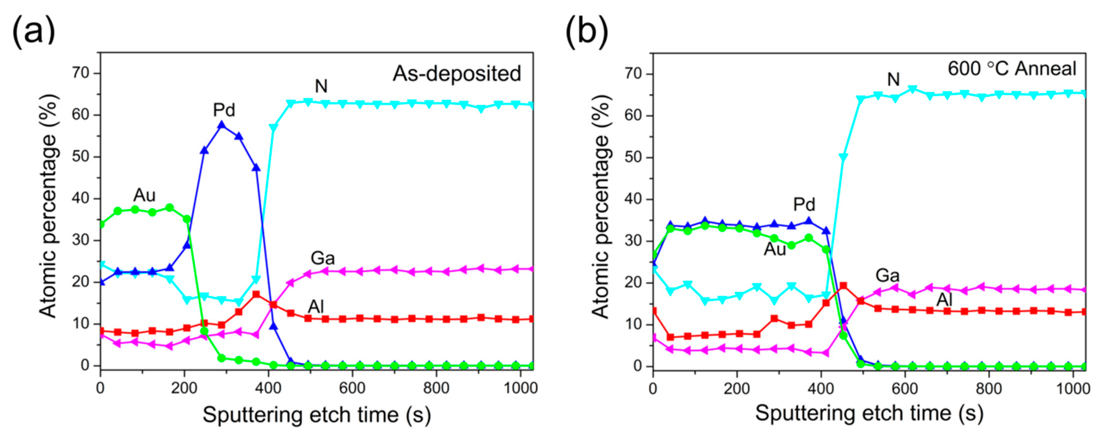
XPS analyses were conducted to elucidate the surface changes at the interface of the PdAl/Au metal stack and p-AlGaN films. Figure 3 shows depth-profiling of the PdAl/Au metal stack before and after annealing at 600 °C. The depth profiling of the as-deposited PdAl/Au metal stack (Figure 3a) shows that the transitions of Pd, Al, and Au films are clearly observable. When the metal stack is annealed at 600 °C, as shown in Figure 3b, a clear variation is observed: compared to the as-deposited contacts, a large quantity of the Ga is out-diffused through the Pd and Au metals. This means that a large chemical reaction occurs between the PdAl metal alloy and Au, and Ga metallic content, which causes the interfacial phases of metallic Ga-Pd and Ga-Au to occur at the interface as confirmed from XRD results (Figure 2b). In addition, there is no clear evidence that the nitrogen content is out-diffused through the metal layers. This indicates that the chemically reacted layers making up the p-AlGaN surface can prevent the out-diffusion of the nitrogen content, which determines the performance of the p-ohmic metal contact. Thus, from the result obtained by XPS depth profiles we confirm that the 600 °C sample shows that the enhancement in the I-V characteristics is due to formation of the Ga-related phases, causing the generation of Ga vacancies near the p-AlGaN surface. Here, Ga vacancies are known to act as acceptors in p-AlGaN.
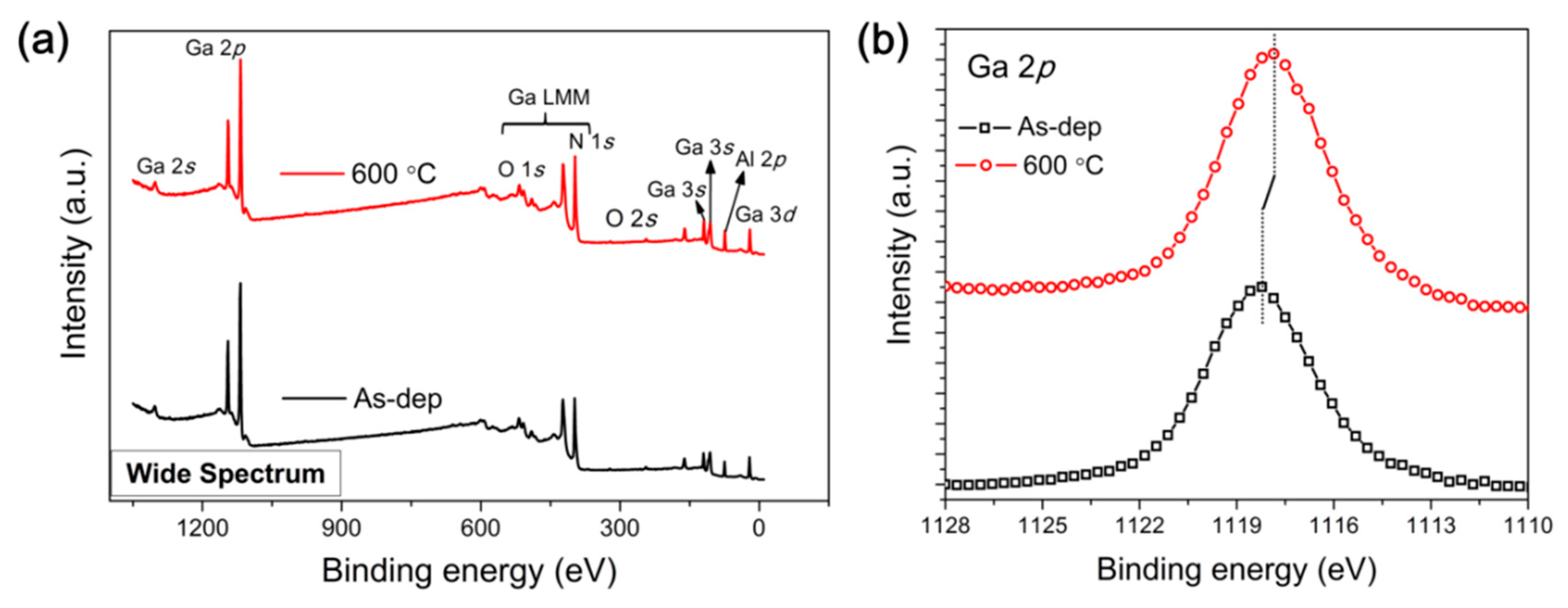
To further analyze the surface spectra of metallic Ga states, XPS measurements are performed before and after annealing at 600 °C. Figure 4a shows a characteristic wide spectrum of the XPS survey, where all core-level and energy features with electronic transitions of Ga, N, and Al are evident. As shown Figure 4b, the Ga-metallic 2p surface-energy-level spectra are found on the interface of PdAl/Au and p-type AlGaN before and after annealing at 600 °C. Unlike the as-deposited contact, the Ga-metallic 2p surface energy level of the annealed contact (600 °C) shifts in the direction of the lower binding energy side. The ~0.36 eV binding energy shift of the metallic Ga 2p XPS peak is observed compared to the as-deposited contact. This behavior is related to the fact that the surface Fermi energy level moves toward the valence band side [16]. The reason for the reduction in energy band bending (i.e., the bending of the surface Fermi energy level toward the valence band side) in the 600 °C annealed contacts could be due to reduction in the Schottky barrier height between the PdAl/Au metals and p-AlGaN films, which results in a low ρc value. This surface Fermi energy-level shift can be initiated to increase Ga vacancies in p-AlGaN, which act like acceptors to enhance the acceptor concentration near the p-AlGaN surface of the annealed contact. A similar influence of annealing was observed in the Pt/Pd/Au and Pd/Au contacts on p-AlGaN [10,11].
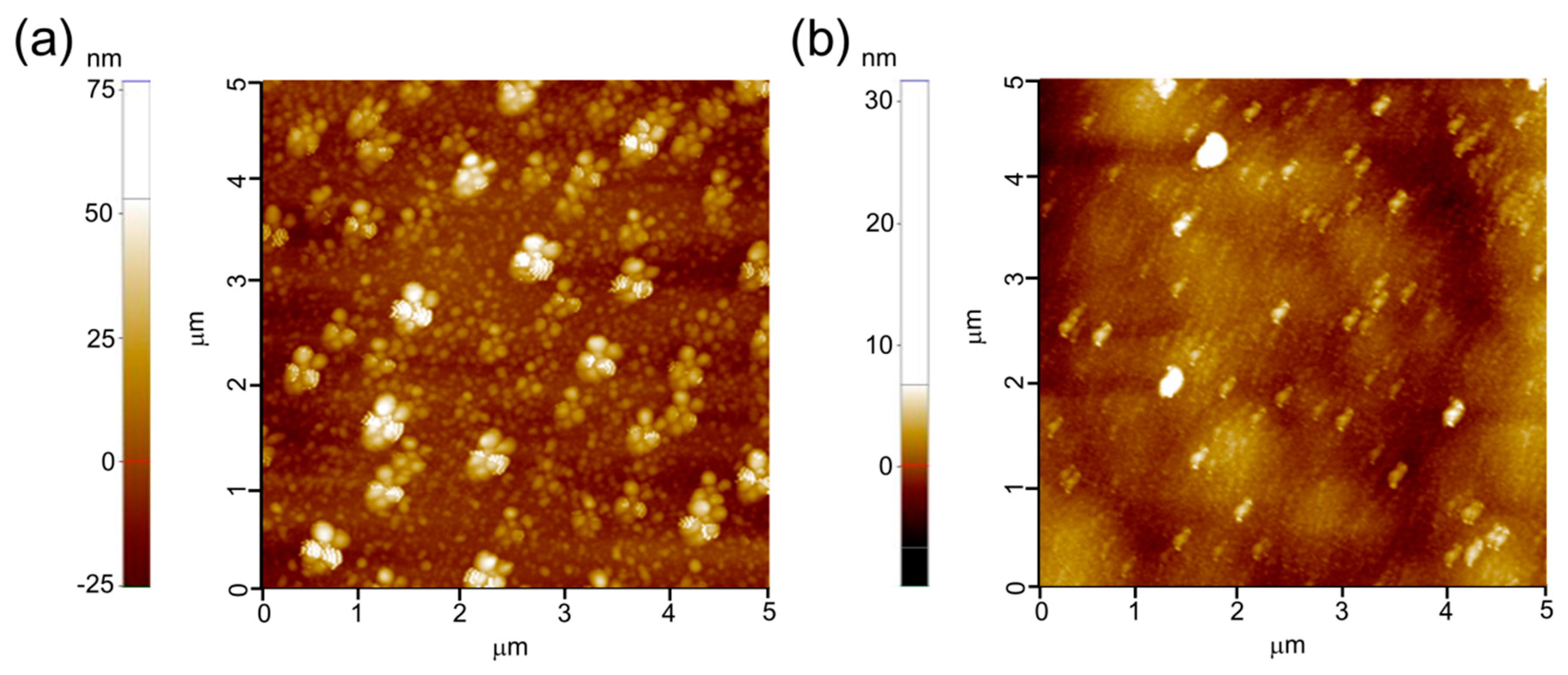
To explain the annealing behavior and understand the mechanism of ohmic contact formation on p-AlGaN, the samples were morphologically characterized using SPM measurements. Figure 5 shows the morphological images of the samples before and after annealing at 600 °C, obtained on a 5 μm × 5 μm (scanned image size). Figure 5a illustrates that the morphological image of the as-deposited contact is a very rough surface, with a root-mean-square (RMS) roughness of 13.53 nm. When the ohmic contact is annealed at 600 °C (Figure 5b), its surface roughness decreases, demonstrating an RMS roughness of 2.89 nm compared to the as-deposited contact. These results indicate that, overall, the surface morphology of PdAl/Au contacts on p-AlGaN is fairly smooth despite the annealing conducted at 600 °C.
4. Conclusions
We experimentally studied the PdAl/Au metal stack on Mg-doped p-AlGaN for fabricating high-performance, highly reliable ohmic contacts. The results revealed that a high-quality ohmic contact was achieved with annealing compared to as-deposited contact. The contact resistance was 1.74 × 10⁻⁴ Ωcm2 when annealed at 600 °C for 1 min in a high-purity N2 atmosphere. XPS and XRD systematic analyses showed that Ga–Pd and Ga–Au phases created when the contacts were annealed at 600 °C causing the generation of Ga vacancies near the p-AlGaN surface were responsible for the enhanced acceptor (hole) concentration near the p-AlGaN surface. The SPM results specified that the RMS roughness of the metal contact was reasonably low for 600 °C annealed contacts. Annealing gives potential benefits of the presence of low-resistance p-ohmic contacts between the PdAl/Au metal stack and p-AlGaN including improved performance.
Author Contributions
Conceptualization, S.P.R.M.; Measurements: S.P.R.M. and W.-H.A., K.-S.I.; Characteristics, S.P.R.M. and W.-H.A., K.-S.I.; Analysis: S.P.R.M., J.-H.L.; Writing, S.P.R.M., J.-H.L.; Supervision, J.-H.L.; funding acquisition, S.P.R.M., J.-H.L. All authors have read and agreed to the published version of the manuscript.
Funding
This research received no external funding.
Acknowledgments
This work was supported by the National Research Foundation of Korea funded by the Ministry of Science, ICT, and Fusion Research (NRF-2018R1D1A1B07040603) and BK21 Plus funded by the Ministry of Education (21A20131600011).
Conflicts of Interest
The authors declare no conflict of interest.
References
- Aoki, Y.; Kuwabara, M.; Yamashita, Y.; Takagi, Y.; Sugiyama, A.; Yoshida, H. A 350-nm-Band GaN/AlGaN Multiple-Quantum-Well Laser Diode on Bulk GaN. Appl. Phys. Lett. 2015, 107, 151103. [Google Scholar] [CrossRef]
- Mallem, S.P.R.; Park, H.; Kim, S.-M.; Jang, S.-H.; Jang, J.-S. High-Performance Light-Emitting Diodes Using Hierarchical M-Plane GaN Nano-Prism Light Extractors. J. Mater. Chem. C 2015, 3, 8873–8880. [Google Scholar]
- Mallem, S.P.R.; Park, W.-S.; Im, K.-S.; Lee, J.-H. Dual-Surface Modification of AlGaN/GaN HEMTs Using TMAH and Piranha Solutions for Enhancing Current and 1/f-Noise Characteristics. J. Electron Dev. Soc. 2018, 6, 791–796. [Google Scholar] [CrossRef]
- Doundoulakis, G.; Adikimennakis, A.; Stavrinidis, A.; Tsagaraki, K.; Androulidaki, M.; Iacovella, F.; Deligeorgis, G.; Konstantinidis, G.; Georgakilas, A. Nanofabrication of Normally-Off GaN Vertical Nanowire MESFETs. Nanotechnlogy 2019, 30, 285304. [Google Scholar] [CrossRef] [PubMed]
- Rauvimov, S.; Liliental-Weber, Z.; Washburn, J.; Qiao, D.; Lau, S.S.; Chu, P.K. Microstructure of Ti/Al Ohmic Contacts for N-AlGaN. Appl. Phys. Lett. 1998, 73, 2582–2584. [Google Scholar] [CrossRef]
- Lim, S.-H.; Washburn, J.; Liliental-Weber, Z.; Qiao, D. Microstructural Evidence on Electrical Properties of Ta/Ti/Al and Ti/Ta/Al Ohmic Contacts to N-AlGaN/GAN. Appl. Phys. Lett. 2001, 78, 3797–3799. [Google Scholar] [CrossRef]
- Bardwell, J.A.; Sproule, G.I.; Liu, Y.; Tang, H.; Webb, J.B.; Fraser, J.; Marshall, P. Comparison of Two Different Ti/Al/Ti/Au Ohmic Metallization Schemes for AlGaN/GaN. J. Vac. Sci. Technol. 2002, 20, 1444–1447. [Google Scholar] [CrossRef]
- Kumar, V.; Zhou, L.; Selvanathan, D.; Adesida, I. Thermally-Stable Low-Resistance Ti/Al/Mo/Au Multilayer Ohmic Contacts on N-GaN. J. Appl. Phys. 2002, 92, 1712–1714. [Google Scholar] [CrossRef]
- Blank, T.V.; Goldberg, Y.A.; Kalinina, E.V.; Konstantinov, O.V.; Nikolaev, A.E.; Fomin, A.V.; Cherenkov, A.E. Mechanism of the Current Flow in Pd-(Heavily Doped P-AlxGa1-xN) Ohmic Contact. Semiconductors 2001, 35, 550–553. [Google Scholar] [CrossRef]
- Jun, B.-H.; Hirayama, H.; Aoyagi, Y. Effect of Thermal Annealing on the Pd/Au Contact to P-Type Al0.15Ga0.85N. Jpn. J. Appl. Phys. 2002, 41, 581–582. [Google Scholar] [CrossRef]
- Kim, H.-K.; Seong, T.-Y.; Adesida, I.; Tang, C.W.; Lau, K.M. Low-Resistance Pt/Pd/Au Ohmic Contacts to P-Type AlGaN. Appl. Phys. Lett. 2004, 84, 1710–1712. [Google Scholar] [CrossRef]
- Chary, I.; Borisov, B.; Kuryatkov, V.; Kudryavtsev, Y.; Asomoza, R.; Nikishin, S.; Holtz, M. Low Resistance Ohmic Contacts to P-Type GaN and AlGaN. Mater. Res. Soc. Symp. Proc. 2009, 1108, 1108-A09-30. [Google Scholar]
- Passow, T.; Gutt, R.; Maier, M.; Pletschen, W.; Kunzer, M.; Schmidt, R.; Wiegert, J.; Luick, D.; Liu, S.; Kohler, K.; et al. Ni/Ag as Low Resistive Ohmic Contact to P-Type AlGaN for UV LEDs. Prof. SPIE 2015, 7617, 76171I-1–76171I-7. [Google Scholar] [CrossRef]
- Hu, Z.F.; Li, X.Y.; Zhang, Y. Characteristics of Ni/Au/Ni/Au Ohmic Contact in a P-AlGaN/GaN Semiconductor. IOP Conf. Ser. Mater. Sci. Eng. 2020, 770, 012018. [Google Scholar] [CrossRef]
- Reddy, V.R. Study of the Electrical, Structural and Surface Morphological Characteristics of Pt/Re/Au Ohmic Contacts on P-Type GaN. Mater. Chem. Phys. 2005, 93, 286–290. [Google Scholar] [CrossRef]
- Sun, J.; Rickert, K.A.; Redwing, J.M.; Ellis, A.B.; Himpsel, F.J.; Kuech, T.F. p-GaN Surface Treatments for Metal Contacts. Appl. Phys. Lett. 2000, 76, 415–417. [Google Scholar] [CrossRef]
Figure 1.
(a) Current–voltage (I–V) curves of the PdAl/Au metal stack contacts to p-AlGaN as a function of annealing temperature. (b) Specific contact resistance (ρc) as a function of annealing temperature of PdAl/Au/p-AlGaN ohmic contacts.
Figure 1.
(a) Current–voltage (I–V) curves of the PdAl/Au metal stack contacts to p-AlGaN as a function of annealing temperature. (b) Specific contact resistance (ρc) as a function of annealing temperature of PdAl/Au/p-AlGaN ohmic contacts.

Figure 2.
X-ray diffraction (XRD) plots of the PdAl/Au metal stack on p-AlGaN (a) as-deposited and (b) annealed at 600 °C.
Figure 2.
X-ray diffraction (XRD) plots of the PdAl/Au metal stack on p-AlGaN (a) as-deposited and (b) annealed at 600 °C.

Figure 3.
Depth-profiling of the PdAl/Au metal stack on p-AlGaN using X-ray photoelectron spectroscopy (XPS): (a) as-deposited and (b) annealed at 600 °C.
Figure 3.
Depth-profiling of the PdAl/Au metal stack on p-AlGaN using X-ray photoelectron spectroscopy (XPS): (a) as-deposited and (b) annealed at 600 °C.

Figure 4.
(a) Wide survey spectrum and (b) Ga 2p energy level of XPS for the PdAl/Au metal stack on p-AlGaN before and after annealing at 600 °C.
Figure 4.
(a) Wide survey spectrum and (b) Ga 2p energy level of XPS for the PdAl/Au metal stack on p-AlGaN before and after annealing at 600 °C.

Figure 5.
Surface morphologies of the PdAl/Au metal stack on p-type AlGaN: (a) as-deposited, and (b) annealed at 600 °C.
Figure 5.
Surface morphologies of the PdAl/Au metal stack on p-type AlGaN: (a) as-deposited, and (b) annealed at 600 °C.


Table 1.
Electrical characteristics of metal alloyed ohmic contact on p-AlGaN with various metallization schemes.
Table 1.
Electrical characteristics of metal alloyed ohmic contact on p-AlGaN with various metallization schemes.
| Metallization Scheme | Annealing Temperature (°C) | Anneal Time (s) | Ambient | ρc (Ωcm2) | Ref |
|---|---|---|---|---|---|
| Pd | 800 | 20 | N2 | – | [9] |
| Pd/Au | 700 | 120 | N2 | – | [10] |
| Pt/Pd/Au | 600 | 60 | N2 | 3.1 × 10⁻⁴ | [11] |
| Au/Ni | 500 | 600 | N2(90%) + O2(10%) | 1.8 × 10⁻⁴ | [12] |
| Ni/Ag/Ni | 450 | – | – | 1.5 × 10⁻² | [13] |
| Ni/Au/Ni/Au | 550 + 750 | 180 + 30 | Air + N2 | – | [14] |
| PdAl/Au | 600 | 60 | N2 | 1.7 × 10⁻⁴ | [This work] |
Publisher’s Note: MDPI stays neutral with regard to jurisdictional claims in published maps and institutional affiliations. |
© 2020 by the authors. Licensee MDPI, Basel, Switzerland. This article is an open access article distributed under the terms and conditions of the Creative Commons Attribution (CC BY) license (http://creativecommons.org/licenses/by/4.0/).
Share and Cite
MDPI and ACS Style
Mallem, S.P.R.; Ahn, W.-H.; Lee, J.-H.; Im, K.-S. Influence of Thermal Annealing on the PdAl/Au Metal Stack Ohmic Contacts to p-AlGaN. Crystals 2020, 10, 1091. https://0-doi-org.brum.beds.ac.uk/10.3390/cryst10121091
AMA Style
Mallem SPR, Ahn W-H, Lee J-H, Im K-S. Influence of Thermal Annealing on the PdAl/Au Metal Stack Ohmic Contacts to p-AlGaN. Crystals. 2020; 10(12):1091. https://0-doi-org.brum.beds.ac.uk/10.3390/cryst10121091
Chicago/Turabian StyleMallem, Siva Pratap Reddy, Woo-Hyun Ahn, Jung-Hee Lee, and Ki-Sik Im. 2020. "Influence of Thermal Annealing on the PdAl/Au Metal Stack Ohmic Contacts to p-AlGaN" Crystals 10, no. 12: 1091. https://0-doi-org.brum.beds.ac.uk/10.3390/cryst10121091
Note that from the first issue of 2016, this journal uses article numbers instead of page numbers. See further details here.