Article

Experimental and Modeling Study on the High-Performance p++-GaAs/n++-GaAs Tunnel Junctions with Silicon and Tellurium Co-Doped InGaAs Quantum Well Inserted

1
College of Electronics and Information Engineering, Sichuan University, Chengdu 610065, China
2
Suzhou Everbright Photonics Co., Ltd., Suzhou 215000, China
*
Author to whom correspondence should be addressed.
Submission received: 26 October 2020 / Revised: 23 November 2020 / Accepted: 24 November 2020 / Published: 28 November 2020
(This article belongs to the Special Issue Organic Conductors)

Abstract

:
The development of high-performance tunnel junctions is critical for achieving high efficiency in multi-junction solar cells (MJSC) that can operate at high concentrations. We investigate silicon and tellurium co-doping of InGaAs quantum well inserts in p++-GaAs/n++-GaAs tunnel junctions and report a peak current density as high as 5839 A cm−2 with a series resistance of 5.86 × 10⁻⁵ Ω cm2. In addition, we discuss how device performance is affected by the growth temperature, thickness, and V/III ratio in the InGaAs layer. A simulation model indicates that the contribution of trap-assisted tunneling enhances carrier tunneling.

Graphical Abstract

1. Introduction

Solar energy is a renewable and environmentally friendly source of energy. Efforts to generate greater electric power from solar energy have benefited from the high efficiency of solar-cell technology [1]. Tunnel junctions are an important component of multi-junction solar cells because they connect the subcells, where each subcell is designed to absorb a specific range within the solar spectrum. Therefore, as the number of subcells increases, the overall absorption of the solar spectrum is enhanced and the thermalization losses are reduced, resulting in a 6-junction solar cell with an efficiency as high as 47.1% [2]. The peak tunneling current density of tunnel junctions must be greater than the photocurrent density of the devices, and the tunnel junctions should have low electrical resistivity and high optical transparency [3].
The peak tunneling current is described below [4]:
J peak exp E g 3 / 2 N eff
where Eg is the energy bandgap of the depletion region, and Neff = (Np++Nn++)/(Np++ + Nn++) is the effective doping concentration, where Np++ and Nn++ are the doping concentrations of the p++and n++ regions, respectively. Equation (1) implies that increased effective doping concentration or a narrower bandgap leads to increased peak tunneling current density. The tunnel-junction resistance is defined as the reciprocal of the initial slope of the J-V curve [4].
The usual way to fabricate tunnel junctions with high peak tunnel-current density and low electrical resistivity is to use highly doped material. Take the p++-GaAs/n++-GaAs tunnel junction as an example: obtaining heavy p-type doping is easily done by using carbon as the dopant. However, it is more complicated for n-type GaAs with a high doping level because, for common epitaxial growth conditions, the compensation and saturation issues of silicon-doped GaAs limits the performance of GaAs tunnel junctions with a doping level around 1 × 1019 cm−3 [5]. Therefore, the peak tunneling current density of silicon-doped GaAs tunnel junctions is around 25 A cm−2 [6]. However, the tunnel junction should be able to operate at current densities up to 90 A cm−2 in a high concentration photovoltaic (HCPV) system (HCPV > 6000 suns, CPV: 500–1000 suns) under non-uniform optical irradiation [7].
A promising way to improve the electrical performance of the tunnel junction is to insert a quantum well (QW) in the p-n interface [8,9]. The band structure of the tunnel junctions with and without quantum well were calculated by solving Poisson’s equation, taking the bandgap narrow into account. As shown in Figure 1, the tunneling distance is shortened with the In0.07GaAs quantum well inserted due to the band offset, so a higher peak tunneling current density can be obtained. However, K. Louarn et al. obtained a peak tunneling current of 30 A cm−2 by using a silicon-doped InGaAs quantum well inserted in a GaAs tunnel junction, which does not satisfy the requirements for the HCPV system [10].
In this work, we proposed the silicon (Si) and tellurium (Te) co-doped InGaAs quantum well inserts in a p++-GaAs/n++-GaAs tunnel junction. Te likely acts as a surfactant that helps the incorporation of Si [11], and Si compensates for the delay time between the injection of DeTe into the reactor and the onset of Te incorporation into the epitaxial layer [12], resulting in a higher doping level in this layer.
The present study investigates the performance of the tunnel junction device, which is affected by the growth conditions of the co-doped InGaAs layer, including the temperature, thickness, and V/III ratio. A peak tunneling current density of 5839 A cm−2 with a resistance of 5.86 × 10⁻⁵ Ω cm2 is achieved in this study. In addition, a simulation model was proposed to investigate the high peak tunneling current density.

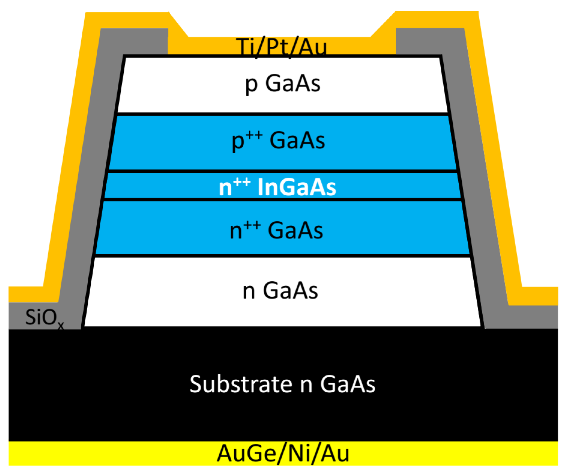
2. Materials and Methods

By using metal-organic chemical vapor deposition (MOCVD), a series of tunnel junctions were grown on (100) n-type GaAs substrates misoriented 6° toward the <111> A direction. We used C (CBr4 source) and Si (Si2H6 source) as p-and n-type dopants, respectively, and the InGaAs quantum well layer was doped with Si and Te (DeTe source). Figure 2 shows a typical tunnel junction structure, which consists of a 30 nm thick n++ (1 × 1019 cm−3) GaAs layer and a 20 nm thick p++ (1 × 1020 cm−3) GaAs layer, with an InGaAs quantum well layer embedded at the p++-n++ junction interface. The doping level was assessed by using the electrical capacitance-voltage (ECV) profile and secondary ion mass spectroscopy (SIMS). The tunnel junction was surrounded by a 150 nm n-type (2 × 1018 cm−3) GaAs buffer layer and a 100 nm p-type (5 × 1019 cm−3) GaAs cap layer on the top to ensure good ohmic contact. The growth conditions of the InGaAs quantum well layer were varied, as summarized in Table 1.
The tunnel junction devices were patterned to different sizes, and chemical etching was used to form square mesa structures of 50 × 50, 100 × 100, 200 × 200, 500 × 500, 1000 × 1000, and 1500 × 1500 µm2. Figure 3 schematically illustrates the device structure. A AuGe/Ni/Au alloyed metal was sputtered onto the backside of the thinned substrates. The devices were fabricated by using conventional photolithographic and wet-etching techniques, and 100 nm SiOx was deposited by plasma-enhanced chemical vapor deposition (PECVD) to isolate the mesa sidewalls. A Ti/Pt/Au top contact metal was deposited by thermal evaporation. To ensure accurate resistance measurements, the four-probe technique was used to measure the J-V curve.

3. Results and Discussion

3.1. Devices Performance of the Tunnel Junctions

We investigated how device performance is affected by growth temperature, thickness, and V/III ratio of the In0.07GaAs layer.

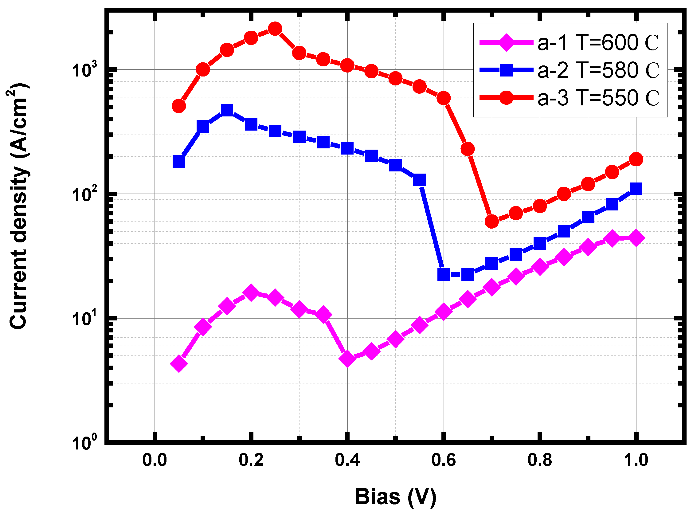
3.1.1. Influence of Growth Temperature

As shown in Figure 4, the J-V curve depends on the growth temperature, with both the peak current density and resistance changes. The results are summarized in rows a-1 to a-3 of Table 2. As the growth temperature decreases from 600 to 550 °C, the peak current density increases from 16 to 2130 A cm−2, and the resistance decreases from 1.25 × 10⁻² to 1.17 × 10⁻⁴ Ω cm2.
The growth temperature is a critical factor for Te incorporation, which occupies the arsenic sublattice, especially when aiming for high doping levels. The decrease in carrier concentration with increasing growth temperature can be explained as follows: As the growth temperature increases, the degree of thermal cracking of arsine increases, arsenic overpressure occurs, and the concentration of arsenic vacancies decreases, which reduces the concentration of substitutional vacancies for tellurium [13].

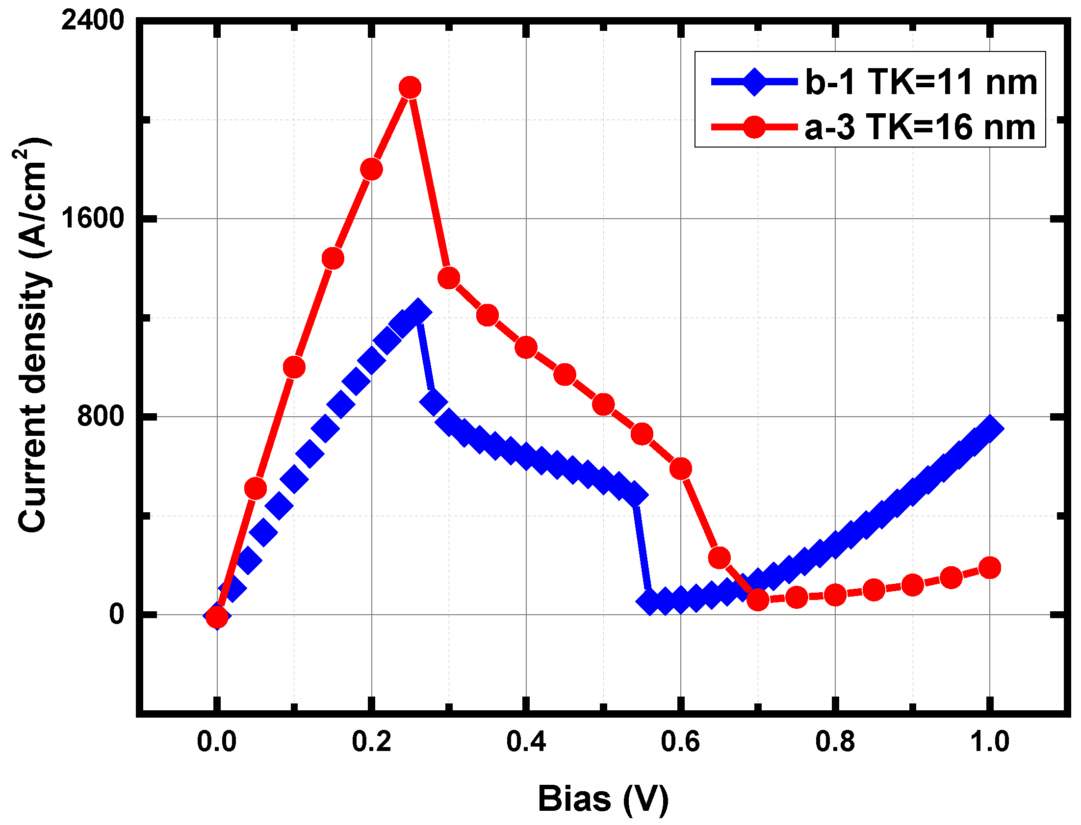
3.1.2. Influence of Thickness

Consider the results shown in Figure 5 and in rows b-1 and a-3 of Table 2. As the In0.07GaAs thickness increases from 11 to 16 nm, the peak current density increases from 1222 to 2130 A cm−2, and the resistance decreases from 1.94 × 10⁻⁴ to 1.17 × 10⁻⁴ Ω cm2.
According to K. Louarn et al. [3], with a thick InGaAs layer, the depletion region expands because the p-side doping concentration exceeds that of the n side. Increasing the thickness of the n-side InGaAs layer reduces the band bending that extends up to the n-GaAs layer and increases the density of states of the direct band-to-band tunneling (DBBT) process [14], resulting in an increased peak tunneling current density because the tunneling probability is increased. With a thin InGaAs layer, a significant band offset occurs at the n++-GaAs/n++-InGaAs interface due to band misalignment, resulting in a quantized energy level due to the potential drop near the tunneling area. Quantum confinement reduces the density of states during the DBBT process, resulting in the reduction of the tunneling probability. Increasing the thickness of the InGaAs quantum well layer reduces the quantum confinement and weakens the discretization of states in the tunnel junction area.

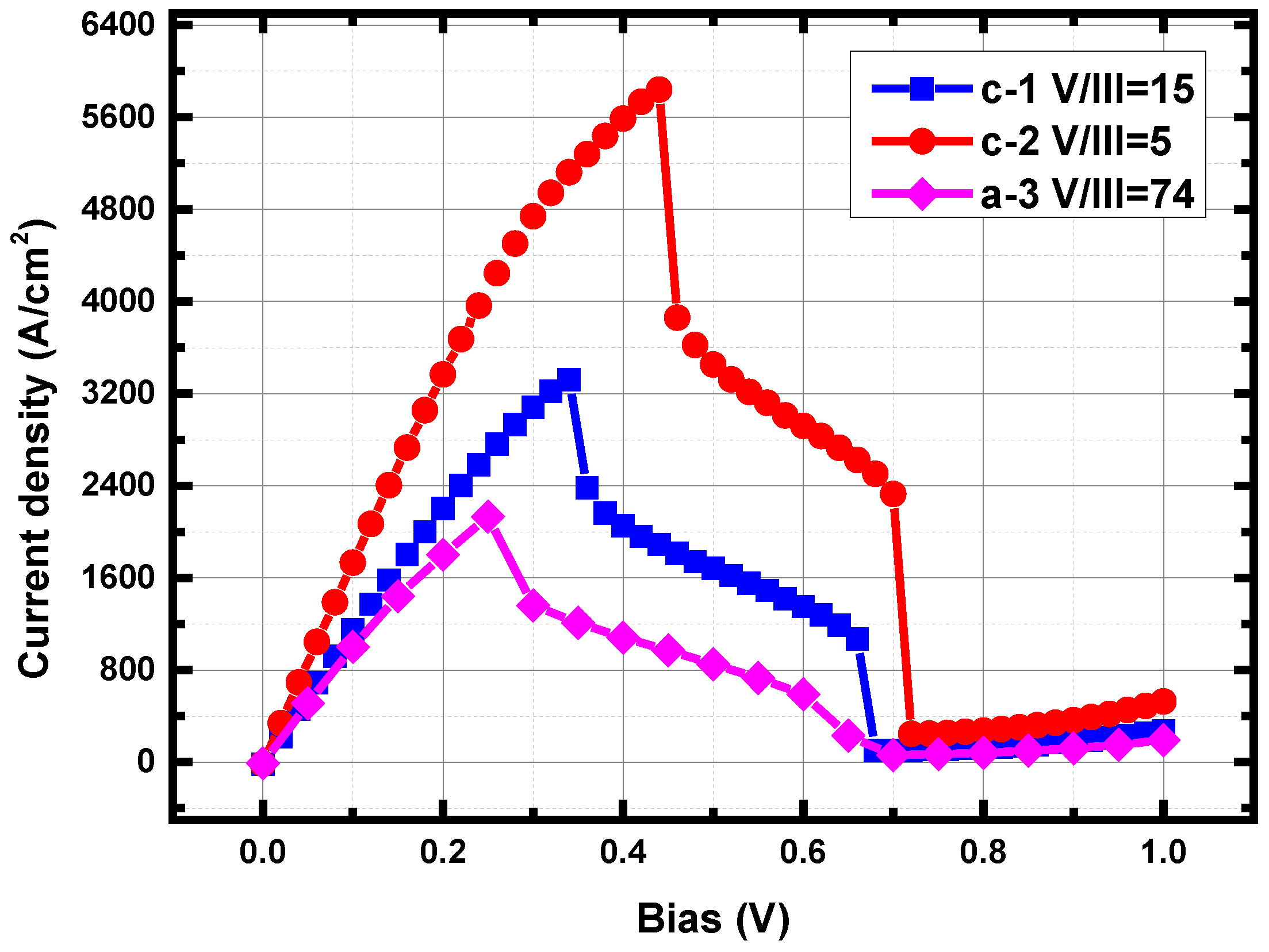
3.1.3. Influence of V/III Ratio

Consider the results shown in Figure 6 and in rows c-1, c-2, and a-3 of Table 2. As the V/III ratio decreases from 74 to 5, the peak current density increases from 2130 to 5839 A cm−2, and the resistance decreases from 1.17 × 10⁻⁴ to 5.86 × 10⁻⁵ Ω cm2.
Decreasing the V/III ratio in the arsine flow at a fixed dopant flow rate increases the probability of the Te substitution into arsenic vacancies due to the fact that Te atoms are n dopants. As shown in Table 2, a higher V/III ratio leads to a lower doping concentration in this layer, we see that lowest V/III ratio used (5), corresponding to a doping concentration up to 5.09 × 1019 cm−3 is reached, which is already above the maximum doping level of 1 × 1019 cm−3 achievable with Si dopant.

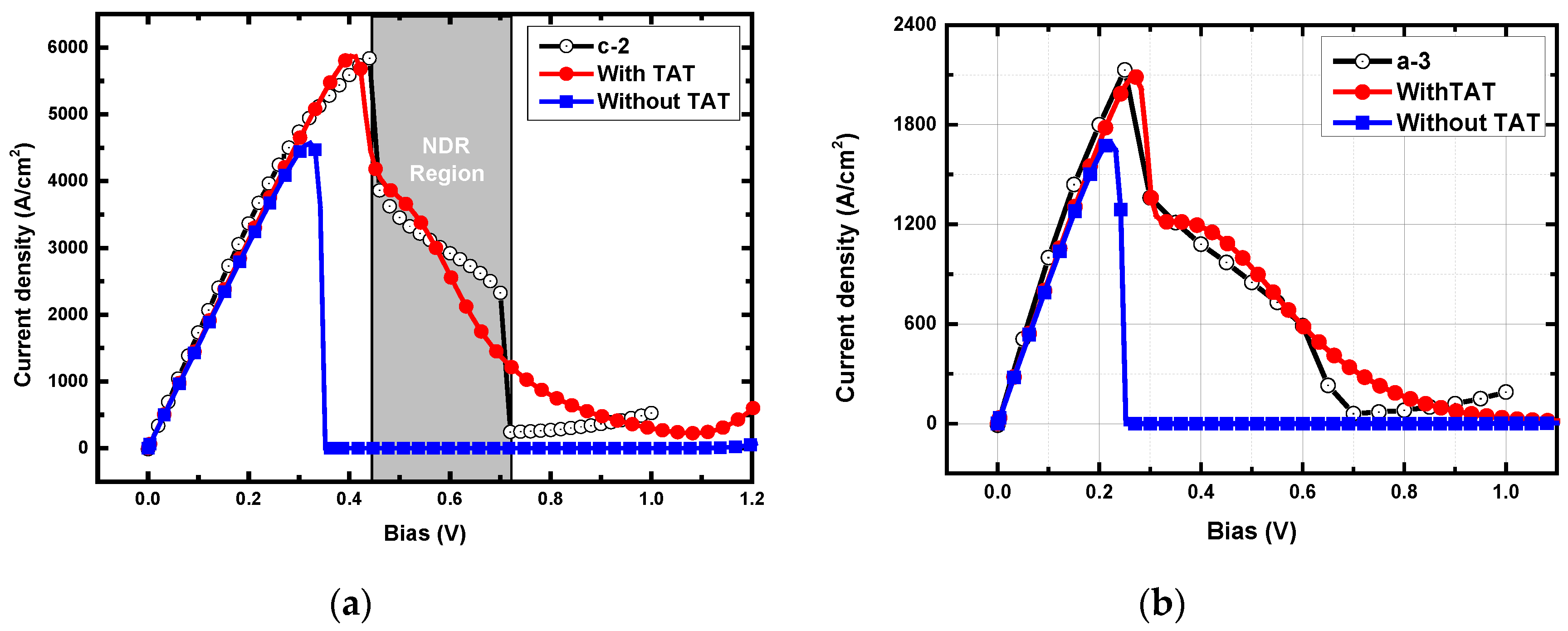
3.2. Role of Trap-Assisted Tunneling

The high peak tunneling current of this study cannot be explained as the usual carrier tunneling due to the doping levels and materials [15]. The contribution of the trap-assisted tunneling mechanism must be considered, which may enhance the carrier tunneling. The heavy doping of the InGaAs layer tends to create clusters [16], and the relaxation of the lattice mismatch between the InGaAs and GaAs layers promotes the formation of defects, which can act as traps in the trap-assisted tunneling (TAT) process [17].
The high peak current density is investigated by using a simulation model implemented in Crosslight APSYS software and that includes a direct band-to-band tunneling [18], bandgap narrowing, and trap-assisted tunneling. In the APSYS simulator, the tunneling probability is solved by Wenzel– Kramers–Brillouin (WKB) approximation and described as following [19]:
D = P 0 exp ( E / E _ )
J ( E ) = x 1 x 2 | ( 2 m 2 ) [ ( E g 2 ) 2 ( ε c ) 2 ] / E g + E | 1 2 d x
P 0 = exp [ π m 1 2 ( E g ) 3 2 2 ( 2 ) 1 2 q F ] = exp ( E g 4 E _ )
E _ = ( 2 ) 1 2 q F 2 π m 1 2 ( E g ) 1 2
where E and E are the electron kinetic energies in perpendicular and parallel to the tunneling direction, respectively, E is a measure of the significance of perpendicular momentum, P0 is the tunneling probability with zero perpendicular momentum, m * is the effective tunneling mass.
With a highly doped InGaAs quantum well inserted in the GaAs tunnel junction, bandgap narrowing should be considered in the model [20]. The bandgap narrowing is expressed as
Δ E g = A { ln N B + [ ( ln N B ) 2 + 1 2 ] 1 2 }
where A and B are constants taken from Slotboom [21], and N is the dopant concentration.
The TAT model is based on the assumption that the traps are able to emit carriers and thus generate a current flux, which is expressed as [22]:
J   =   q   N trap d d F ( S TAT f T ) Δ V
where STAT is the emission rate, Ntrap is the bulk trap density, F is the electrical field, fT is a correction factor due to temperature, related to thermal activation of trapped carriers. The Poole-Frenkel model of field dependence is implemented [22], where the Poole-Frenkel shift of the trap level is expressed as:
Δ E PF = q F π ϵ 0 ϵ
To adapt the high peak tunneling current of the sample c-2, two free changeable parameters: the trap carrier lifetimes (tn, tp) and the Poole–Frenkel shift (ΔEPF) are used to calibrate the simulation model. Figure 7 shows how the model be tuned to get a good agreement between the simulated and experimental results, including peak tunneling current values and the secondary peak values. With lower tp and higher Poole-Frenkel shifts, the peak tunneling current values and secondary peak values increase. The simulation results are consistent with experimental data for trap carrier lifetimes of tn = 0.45 × 10⁻⁴ s and tp = 4 × 10⁻² s, and with a Poole-Frenkel shift in the trap level of 1.41 eV, respectively. However, the simulation results are not consistent with the experimental data in the region of negative differential resistance (NDR) because of the instability of the secondary peak [23], which is probably caused by the “two-step” tunneling through the trap states [24]. However, Figure 8 shows that the peak tunneling current density decreases if the TAT effect is not taken into account, which indicates that the trap-assisted tunneling enhances the peak tunneling current values.

4. Conclusions

We implement Si and Te co-doped InGaAs quantum well inserts in a GaAs tunnel junction and obtain the result with a peak current density as high as 5839 A cm−2 and a series resistance of 5.86 × 10⁻⁵ Ω cm2. The performance of the devices is investigated at various growth conditions of the InGaAs layer, including the growth temperature, thickness, and V/III ratio. A simulation model is used to investigate the performance of the devices, and the results indicate that the trap-assisted tunneling contributes to increasing the peak tunneling current.

Author Contributions

Conceptualization, Y.G. (Yudan Gou) and J.W.; methodology, Y.G. (Yudan Gou); software, Y.G. (Yudan Gou); validation, Y.C., and Y.G. (Yudan Gou); formal analysis, Y.G. (Yudan Gou); investigation, Y.G. (Yudan Gou), X.X., S.Z., L.Z. and J.W.; resources, J.W.; data curation, Y.G. (Yudan Gou); writing—original draft preparation, Y.G. (Yudan Gou); writing—review and editing, G.D., H.Y., H.L., S.T., Y.C., Y.G. (Yintao Guo), X.X., S.Z.; visualization, Y.G. (Yudan Gou) and J.W.; supervision, J.W.; project administration, Y.G. (Yudan Gou) and J.W. All authors have read and agreed to the published version of the manuscript.

Funding

This research received no external funding.

Acknowledgments

The authors thank Sheng Yang and Xia Changsheng from the Crosslight software Inc. for helpful discussions regarding this work.

Conflicts of Interest

The authors declare no conflict of interest.

References

  1. Kabir, E.; Kumar, P.; Kumar, S.; Adelodun, A.A.; Kim, K.H. Solar energy: Potential and future prospects. Renew. Sustain. Energy Rev. 2018, 82, 894. [Google Scholar] [CrossRef]
  2. Geisz, J.F.; France, R.M.; Schulte, K.L.; Steiner, M.A.; Norman, A.G.; Guthrey, H.L.; Young, M.R.; Song, T.; Moriarty, T. Six-junction III–V solar cells with 47.1% conversion efficiency under 143 Suns concentration. Nat. Energy 2020, 5, 326. [Google Scholar] [CrossRef]
  3. Louarn, K.; Claveau, Y.; Fontaine, C.; Arnoult, A.; Marigo-Lombart, L.; Massiot, I.; Piquemal, F.; Bounouh, A.; Cavassilas, N.; Almuneau, G. Thickness Limitation of Band-to-Band Tunneling Process in GaAsSb/InGaAs Type-II Tunnel Junctions Designed for Multi-Junction Solar Cells. ACS Appl. Energy Mater. 2019, 2, 1149. [Google Scholar] [CrossRef] [Green Version]
  4. Wheeldon, J.F.; Valdivia, C.E.; Walker, A.W.; Kolhatkar, G.; Jaouad, A.; Turala, A.; Riel, B.; Masson, D.; Puetz, N.; Fafard, S.; et al. Performance comparison of AlGaAs, GaAs and InGaP tunnel junctions for concentrated multijunction solar cells. Prog. Photovolt. 2011, 19, 442. [Google Scholar] [CrossRef]
  5. Northrup, J.E.; Zhang, S.B. Dopant and defect energetics: Si in GaAs. Phys. Rev. B 1993, 47, 6791. [Google Scholar] [CrossRef] [PubMed]
  6. Hermle, M.; Létay, G.; Philipps, S.P.; Bett, A.W. Numerical simulation of tunnel diodes for multi-junction solar cells. Prog. Photovolt. 2008, 16, 409. [Google Scholar] [CrossRef]
  7. Bedair, S.; Carlin, C.Z.; Harmon, J.L.; Sayed, I.E.H.; Colter, P. High Performance Tunnel Junction with Resistance to Thermal Annealing. In Proceedings of the 12th International Conference on Concentrator Photovoltaic Systems (CPV-12), Freiburg, Germany, 25–27 April 2016; p. 020003. [Google Scholar]
  8. Lumb, M.P.; Yakes, M.K.; Gonzalez, M.; Vurgaftman, I.; Bailey, C.G.; Hoheisel, R.; Walters, R.J. Double quantum-well tunnel junctions with high peak tunnel currents and low absorption for InP multi-junction solar cells. Appl. Phys. Lett. 2012, 100, 213907. [Google Scholar] [CrossRef]
  9. Bedair, S.; Harmon, L.J.; Carlin, C.Z.; Hashem, I.E.; Colter, P.C. High performance as-grown and annealed high band gap tunnel junctions: Te behavior at the interface. Appl. Phys. Lett. 2016, 108, 203903. [Google Scholar] [CrossRef] [Green Version]
  10. Louarn, K.; Claveau, Y.; Marigo-Lombart, L.; Fontaine, C.; Arnoult, A.; Piquemal, F.; Bounouh, A.; Cavassilas, N.; Almuneau, G. Effect of low and staggered gap quantum wells inserted in GaAs tunnel junctions. J. Phys. D Appl. Phys. 2018, 51, 145107. [Google Scholar] [CrossRef]
  11. Law, J.J.M.; Carter, A.D.; Lee, S.; Huang, C.Y.; Lu, H.; Rodwell, M.J.W.; Gossard, A.C. Co-doping of InxGa1-xAs with silicon and tellurium for improved ultra-low contact resistance. J. Cryst. Growth 2013, 378, 92. [Google Scholar] [CrossRef]
  12. Nguyen, X.S.; Yadav, S.; Lee, K.H.; Kohen, D.; Kumar, A.; Made, R.I.; Lee, K.E.K.; Chua, S.J.; Gong, X.; Fitzgerald, E.A. MOCVD growth of high quality InGaAs HEMT layers on large scale Si wafers for heterogeneous integration with Si CMOS. IEEE Trans. Semicond. Manuf. 2017, 30, 456. [Google Scholar] [CrossRef]
  13. Hamon, G.; Paillet, N.; Alvarez, J.; Larrue, A.; Decobert, J. Te doping of GaAs and GaInP using diisopropyl telluride (DIPTe) for tunnel junction applications. J. Cryst. Growth 2018, 498, 301. [Google Scholar] [CrossRef]
  14. Louarn, K. Development of Tunnel Junctions Based on III-V Semiconductors Heterostructures for High Efficiency Multi-Junction Solar Cells. Ph.D. Thesis, Paul Sabatier University, Toulouse, France, 2018. [Google Scholar]
  15. Jandieri, K.; Baranovskii, S.D.; Rubel, O.; Stolz, W.; Gebhard, F.; Guter, W.; Hermle, M.; Bett, A.W. Resonant electron tunneling through defects in GaAs tunnel diodes. J. Appl. Phys. 2008, 104, 094506. [Google Scholar] [CrossRef]
  16. Park, Y.; Qian, W.; Skowronski, M. Precipitation of Tellurium-Rich Phase in Heavily Diethyltellurium-Doped GaAs during Organometallic Vapor Phase Epitaxy. J. Electrochem. Soc. 1995, 142, 4294. [Google Scholar] [CrossRef]
  17. García, I.; Rey-Stolle, I.; Algora, C. Performance analysis of AlGaAs/GaAs tunnel junctions for ultra-high concentration photovoltaics. J. Phys. D Appl. Phys. 2012, 45, 045101. [Google Scholar]
  18. Crosslight Software Inc., Canada. Available online: http://www.crosslight.com/ (accessed on 20 October 2019).
  19. Li, Z.Q.; Xiao, Y.G.; Li, Z.M.S. Modeling of multi-junction solar cells by Crosslight APSYS. In High and Low Concentration for Solar Electric Applications; International Society for Optics and Photonics: San Diego, CA, USA, 2006; p. 633909. [Google Scholar]
  20. Colter, P.; Hagar, B.; Bedair, S. Tunnel junctions for III-V multijunction solar cells review. Crystals 2018, 8, 445. [Google Scholar] [CrossRef] [Green Version]
  21. Slotboom, J.W.; Degraaff, H.C. Measurements of bandgap narrowing in Si bipolar transistors. Solid-State Electron. 1976, 19, 857. [Google Scholar] [CrossRef]
  22. Gehring, A. Simulation of Tunneling in Semiconductor Devices. Ph.D. Thesis, Technical University, Vienna, Austria, 2003. [Google Scholar]
  23. Wheeldon, J.F.; Valdivia, C.E.; Walker, A.; Kolhatkar, G.; Hall, T.J.; Hinzer, K.; Masson, D.; Fafard, S.; Jaouad, A.; Turala, A. AlGaAs tunnel junction for high efficiency multi-junction solar cells: Simulation and measurement of temperature-dependent operation. In Proceedings of the 34th IEEE Photovoltaic Specialists Conference (PVSC), Philadelphia, PA, USA, 7–12 June 2009; pp. 106–111. [Google Scholar]
  24. Narasimhan, V.K.; Yastrebova, N.; Valdivia, C.E.; Hall, T.J.; Hinzer, K.; Masson, D.; Fafard, S.; Jaouad, A.; Arès, R.; Aimez, V. Effect of parameter variations on the current-voltage behavior of AlGaAs tunnel junction models. In Proceedings of the 1st Microsystems and Nanoelectronics Research Conference, Ottawa, ON, Canada, 15 October 2008; p. 165. [Google Scholar]
Figure 1. Band structure of (1) p++-GaAs//n++-In0.07GaAs/n++-GaAs (solid line) and (2) p++-GaAs/n++-GaAs (dashed line) tunnel junctions. The differences in band bending shorten the tunneling distance for the InGaAs quantum well inserted in the GaAs tunnel junction structure.
Crystals 10 01092 g001
Figure 2. Schematic of tunnel-junction structure. The growth conditions of the InGaAs layer are summarized in Table 1.
Crystals 10 01092 g002
Figure 3. Schematic illustration of the tunnel-junction device structure.
Crystals 10 01092 g003
Figure 4. Experimental results of tunnel-junction devices under various growth temperature of the In0.07GaAs layer.
Crystals 10 01092 g004
Figure 5. Experimental results of tunnel-junction devices under various thickness of the In0.07GaAs layer.
Crystals 10 01092 g005
Figure 6. Experimental results of tunnel-junction devices under various V/III ratio for the In0.07GaAs layer.
Crystals 10 01092 g006
Figure 7. Influence of (a) trap carrier lifetime and (b) Poole–Frenkel shift on simulated J-V curve. The experimental data are from sample c-2.
Crystals 10 01092 g007
Figure 8. Simulated J-V curve with and without using the trap-assisted tunneling (TAT) model. The experimental data is from the sample (a) c-2 and (b) a-3.
Crystals 10 01092 g008
Table 1. Summary of growth conditions for In0.07GaAs layer.
Sample No.Thickness (nm)V/IIITemperature (°C)
a-11674600
a-21674580
a-31674550
b-11174550
c-11615550
c-2165550
Table 2. Summary of experimental results.
Sample No.Doping Level (cm−3)Peak Current Density (A cm−2)Resistance (Ω cm2)
a-11.13 × 1019161.25 × 10−2
a-22.00 × 10194723.17 × 10−4
a-34.03 × 101921301.17 × 10−4
b-13.55 × 101912221.94 × 10−4
c-14.22 × 101933209.00 × 10−5
c-25.09 × 101958395.86 × 10−5
Publisher’s Note: MDPI stays neutral with regard to jurisdictional claims in published maps and institutional affiliations.

