Article

Light Extraction Enhancement Techniques for Inorganic Scintillators

1
Advanced Quantum Architecture Lab (AQUA), École Polytechnique Fédérale de Lausanne (EPFL), 2002 Neuchâtel, Switzerland
2
NAPA-Technologies, 74160 Archamps, France
3
Laboratoire Lumière, Nanomatériaux et Nanotechnologie, CNRS ERL 7004, Université de Technologie de Troyes, 12 rue Marie Curie, 10004 Troyes CEDEX, France
4
Photovoltaics and Thin Films Electronics Laboratories (PV-LAB), École Polytechnique Fédérale de Lausanne (EPFL), 2002 Neuchâtel, Switzerland
*
Author to whom correspondence should be addressed.
Submission received: 3 March 2021 / Revised: 22 March 2021 / Accepted: 25 March 2021 / Published: 30 March 2021
(This article belongs to the Special Issue Scintillator & Phosphor Materials)

Abstract

:
Scintillators play a key role in the detection chain of several applications which rely on the use of ionizing radiation, and it is often mandatory to extract and detect the generated scintillation light as efficiently as possible. Typical inorganic scintillators do however feature a high index of refraction, which impacts light extraction efficiency in a negative way. Furthermore, several applications such as preclinical Positron Emission Tomography (PET) rely on pixelated scintillators with small pitch. In this case, applying reflectors on the crystal pixel surface, as done conventionally, can have a dramatic impact of the packing fraction and thus the overall system sensitivity. This paper presents a study on light extraction techniques, as well as combinations thereof, for two of the most used inorganic scintillators (LYSO and BGO). Novel approaches, employing Distributed Bragg Reflectors (DBRs), metal coatings, and a modified Photonic Crystal (PhC) structure, are described in detail and compared with commonly used techniques. The nanostructure of the PhC is surrounded by a hybrid organic/inorganic silica sol-gel buffer layer which ensures robustness while maintaining its performance unchanged. We observed in particular a maximum light gain of about 41% on light extraction and 21% on energy resolution for BGO, a scintillator which has gained interest in the recent past due to its prompt Cherenkov component and lower cost.

1. Introduction

Scintillating materials are commonly used in high energy physics and medical applications because of their capability to downconvert high energy radiation into optical photons. Scintillators are usually instrumented with a photosensor and coupled to its sensitive surface. Originally, Photomultiplier Tubes (PMTs) were the most used photodetectors to read out the scintillation light, but nowadays silicon-based devices such as Silicon Photomultipliers (SiPMs) have moved into a prominent position. This trend is due to their more compact structure, lower supply voltage, and robustness to magnetic fields. The light sensitivity of both PMTs and SiPMs do usually not exceed 30% at short wavelengths (e.g., 300 nm) in commercial devices [1], and peaks at around 50–60% in the visible for SiPMs [2]. The amount of light generated during the scintillation process in inorganic scintillators is in the range 8–60 k photons/MeV (e.g., the LYSO light yield is around 30 k photons/MeV) [3,4]. However, in standard configurations only a small percentage of this light reaches the photodetector. Extracting as much light as possible from the crystal becomes thus crucial, given that both energy and time resolution depend strongly on the amount of detected light. Indeed, extracting more light enables a more accurate estimation of the energy deposited in the crystal by the incoming radiation, which in turn allows a better discrimination of events that underwent Compton scattering. Moreover, the Coincidence Resolving Time (CRT), which represents the Full-width at Half-maximum (FWHM) of the distribution of the time difference between two events in coincidence, has been demonstrated to be proportional to the inverse square root of the amount of detected photons [5,6].
Several phenomena limit the amount of light that can be extracted from the crystal and then detected by a photodetector. These include, at the scintillator-photodetector interface (Figure 1a–c), the actual light collection efficiency, which determines the amount of light that reaches the active area of the photodetector, as well as total internal reflection and Fresnel losses. In addition, light absorption in the scintillator itself affects the number of photons that are lost along their path to the output surface of the crystal, with the absorption length reducing at shorter wavelengths [3].
Moreover, if not covered by any material, the scintillator can let light escape through its lateral surfaces, thus losing a significant amount of optical photons (Figure 2, left). A solution to overcome this problem is to confine the scintillation light inside the scintillator and redirect the optical photons toward the output surface. One possibility is to apply a specular reflector to the lateral surfaces (Figure 2, right). However, in such a scenario most of the light generated during scintillation cannot be extracted and remains trapped inside the crystal until it gets absorbed. This phenomenon is due to the relatively large difference of refractive index between the scintillator (e.g., 1.8 for LYSO and 2.15 for BGO at the peak emission), the air (n = 1) between crystal and detector, and the photosensor window (typically 1.4–1.5 for glass) coupled on its surface. To mitigate this effect, an optimization of the optical coupling is possible, e.g., by means of refractive index matching compounds such as greases or waxes; the latter can increase the critical angle of total internal reflection, allowing the extraction of more light (Figure 2, right). Another possibility is represented by the use of diffusors on the scintillator surfaces, which redirect the impinging photons after each reflection (Figure 3 left). This results in a decrease of the total internal reflection probability at the output surface, with a higher chance of the scintillation photons being extracted at the first interaction such an indirect redirection scheme does however not prevent internal absorption from occurring. A more sophisticated approach has also been proposed, which relies on the redirection within the escape cone of the photons which impinge on the lateral surfaces, by means of diffraction gratings whose periodicity has been specifically designed [7]. This approach has not yet been implemented.
In this work we analyze, combine, and compare several conventional as well as novel light extraction techniques, especially targeted for Positron Emission Tomography (PET) applications, applied to two conventional inorganic scintillators, namely LYSO and BGO. While LYSO is the scintillator of reference in Time-of-Flight PET (ToF-PET), BGO has seen renewed interest in the recent past mostly due to the possibility of detecting the small but prompt Cherenkov emission component thanks to impressive progress in SiPM performance [8]. BGO features a higher attenuation coefficient and photoelectric fraction than LYSO as well as lower cost, but suffers from lower light yield and a slower scintillation component. However, it is highly transparent down to 310 nm and has a high refractive index of about 2.15 at the peak emission wavelength (480 nm), which are expected to make it a good Cherenkov radiator.
The novel techniques, which we investigated include the use of Photonic Crystals (PhCs) nanoimprinted on the crystal output surface, as well as Distributed Bragg Reflectors (DBRs) and metal coatings applied to the other crysal surfaces. We studied in particular a modified photonic crystal structure, designed to increase its structural robustness against mechanical stress while ensuring performance gains under realistic conditions similar to those often reported with air-coupled scenarios. The DBRs were simulated prior to fabrication and two different structures were compared, namely a conventional mirror centered on the BGO scintillation spectrum, and one whose reflectivity extends to the NUV, coupled to a silver mirror. The experimental set-up consisted of sets of 10 × 10 × 10 mm 3 crystal samples coupled to a PMT, interfaced to a Multi-Channel Analyzer (MCA), to ensure reproducibility and ease of use. An analysis of the results and a final discussion close the paper.

2. Light Extraction Techniques: State-of-the-Art

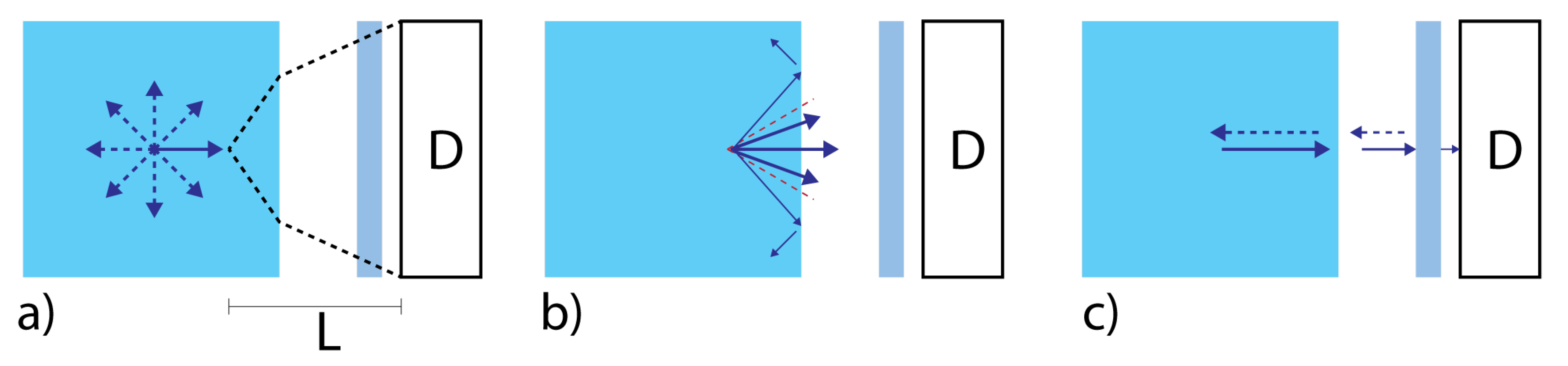
2.1. Conventional Light Extraction Enhancement Techniques

In current radiation detectors based on scintillators, one of the most commonly used techniques to overcome the lateral light losses consists in the use of Teflon wrapping (Figure 3 left). This material is cheap and easily available. It is typically applied on five of the six surfaces of the crystal and acts as a light diffuser, whereby its properties also depend on the thickness of the applied layer [9,10]. A detailed study of the influence of Teflon wrapping on scintillators can be found in [11,12].
The adoption of this solution, using a sufficiently thick layer of Teflon (larger than 100 μ m) on the sidewalls to ensure enough reflectivity (>80%) [9,10], can dramatically improve the light extraction efficiency of the system, even if it appears to be unsuitable for applications in which the crystal is pixelated in small needles. This is for example the case for preclinical PET scanners [13], which typically rely on small pitch (sub-millimeter) scintillators to increase the spatial resolution. Indeed, as shown in Figure 4, the efficiency of the system is quickly reduced when the crystal size becomes comparable to the size of the coating due to the reduced packing fraction (ratio of crystal cross-section without coating to cross-section with coating).
This geometric effect can be mitigated by changing the scattering behavior and resorting to other materials such as the Enhanced Specular Reflector (ESR) [14], which features a typical thickness of 65 μ m; its analysis is reported in [15]. The ESR is a film of dielectric material (Figure 3 right) with high reflectivity over a very large spectrum, and represents the current gold standard when reflective coatings are applied on scintillator surfaces. However, its reflectivity drops at 400 nm, limiting its use in those cases when the emission spectrum of scintillators is shifted toward the blue-Near Ultraviolet (NUV) range. Figure 3 illustrates a visual comparison between the two aforementioned reflectors.
However, as discussed in the Introduction, the use of reflectors alone is not sufficient. Indeed, very few systems are air-coupled—almost all practical PET implementations rely on an optimization of the optical interface between crystal and detector to mitigate the light losses at the photosensor interface. This is typically achieved by applying a refractive index matching material to smooth the refractive index (n) transition and increase the critical angle, thereby reducing the amount of light that undergoes total internal reflection and Fresnel losses. Several solutions are available with different refractive indices depending on the target scintillator. The compounds being used (especially during prototyping and research) are often in the form of waxes or greases because they are practical to employ and guarantee a good degree of system stability. These compounds provide high transmittance also at a short wavelength and a refractive index usually comprised between 1.4 and 1.6.

2.2. Novel Light Extraction Enhancement Techniques

Recently, the use of nanostructures applied to the output surface of the scintillator, commonly called Photonic Crystals (PhC), has been investigated for PET applications [16,17,18]. Photonic crystals are periodic structures of hundreds of nanometers in size directly built on the output surface of the scintillator. Their principle of operation relies on scattering the light photons at the interfaces of materials with a different refractive index. The scattered waves interact constructively or destructively (depending on the structure) with each other. The coating acts as a diffraction grating and leads to higher extraction efficiency, de facto overcoming the limitations of total internal reflection described by Snell’s law [17]. Initial developments have relied on e-beam lithography, which is very accurate but usually slow and very costly, moving then to nanoimprint with the potential of large area coverage, process simplification, and cost reduction; self-assembly techniques have also been employed more recently. These structures rely on a high refractive index contrast between the nanostructure and the surrounding medium, leading to interesting optical properties especially if applied on the surface of high refractive index material. Indeed, PhCs have shown to be capable of increasing the amount of light extracted from inorganic scintillators, albeit to varying degrees and under often quite different experimental conditions, such as for LSO [17], LYSO [19,20,21,22] (self-assembly and e-beam, and nanoimprint), GYGAG and S r I 2 [23] (nanoimprint), CsI(Na) [24,25], and BGO [26] (self-assembly). A more comprehensive description of the PhC physics is reported in [17,18]. Their use has also been suggested by our group in combination with microlensed SiPMs [27], whereby the two components would work in synergy, with the PhCs reducing the angular spread of the scintillation light, thereby increasing the efficiency of the microlenses.
However, the PhC structures have been mostly optimized and tested using air coupling with the photodetector optical window [21], in some cases with techniques that do not scale to large patterning areas. In addition, their structure is very fragile and not suitable to be used easily and reliably in standard configurations, in which a refractive index matching compound is employed between the crystal and sensor optical window. Indeed, the shear stress created during the coupling process can easily damage the nanostructure, thereby compromising its performance and measurement repeatability. Moreover, the PhC architecture, as mentioned, is very sensitive to the refractive index contrast, and the use of optical grease can compromise the effectiveness of the solution [17]. To overcome this issue, in this study we elaborated a nanoimprint-based solution that uses a hybrid organic/inorganic (O/I) silica sol-gel buffer layer (n = 1.46) which encapsulates the nanostructure. This approach ensures structural robustness and maintains the PhC performance unvaried (Figure 5).
In addition to the core work on improved photonic crystals, the use of thin film coatings, such as DBR [28,29,30] and metal coatings (Al and Ag), was explored to overcome the aforementioned limitations on the packing fraction. A DBR (Figure 6) is a very thin (order of 1 μ m) periodic structure formed by alternating quarter wavelength stacks of dielectric layers. The reflectivity spectral width depends on the refractive index contrast of the materials used and is tunable. A DBR typically contains a large number of layers with a high refractive index contrast. It can be used to achieve nearly total reflection within a range of wavelengths, and it is thus employed as a reflector in waveguides and optical fibers, presenting extremely low losses compared to ordinary metallic mirrors [31]. Each interface between the two materials contributes a Fresnel reflection. At the design wavelength, the optical path length difference between reflections from subsequent interfaces is half the wavelength, in addition, the reflection coefficient amplitudes for the interfaces have alternating signs. Therefore, all reflected components interfere constructively, which results in a strong reflection.
The reflectivity achieved is determined by the number of layer pairs and by the refractive index contrast between the layer materials. However, because of their stratification, the reflectivity of the DBR turns out to be highly angular dependent. Indeed, the reflectivity changes significantly for incidence angles above 30°. It is worth mentioning here the possibility of using the so-called perfect or omnidirectionnal mirrors which reflect light whatever the angle of incidence and polarization, assuming that the average refractive index of the DBR is higher than the one of the scintillating crystal [32]. This approach has however not yet been used for scintillating crystals. Finally, it is worth noting that DBRs can be combined with metal layers to enhance the reflectivity spectrum especially at long wavelengths, while at the same time compensating the loss of reflectance below 450 nm typical of metal mirrors.

3. Materials and Methods

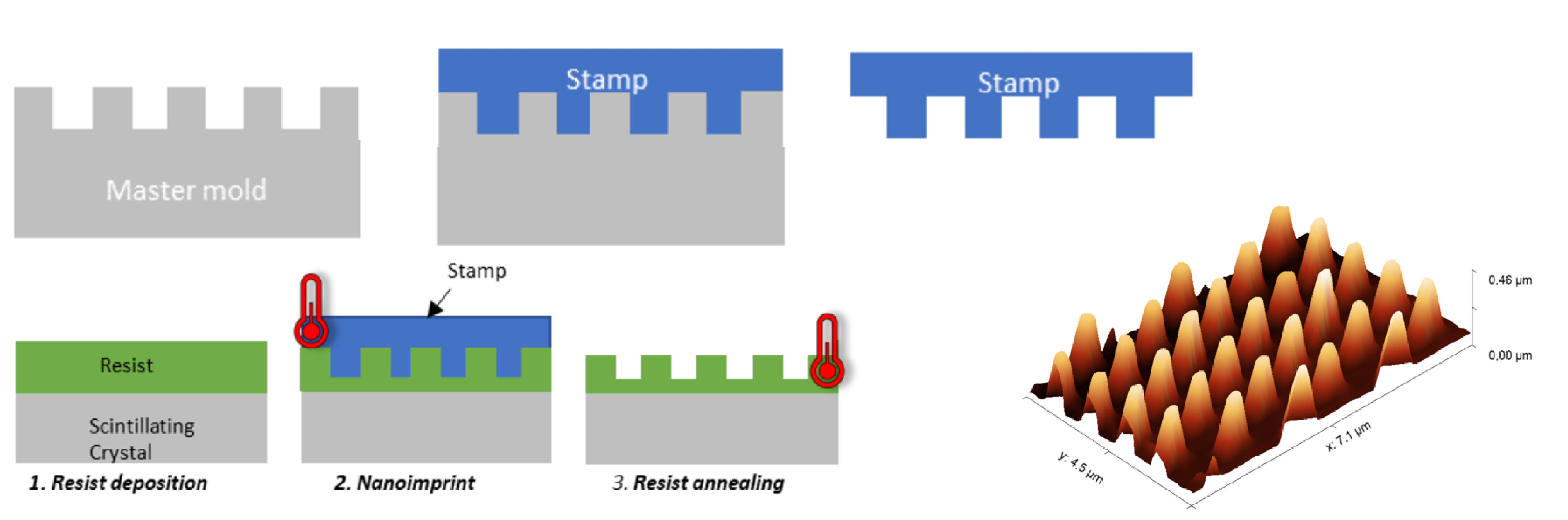
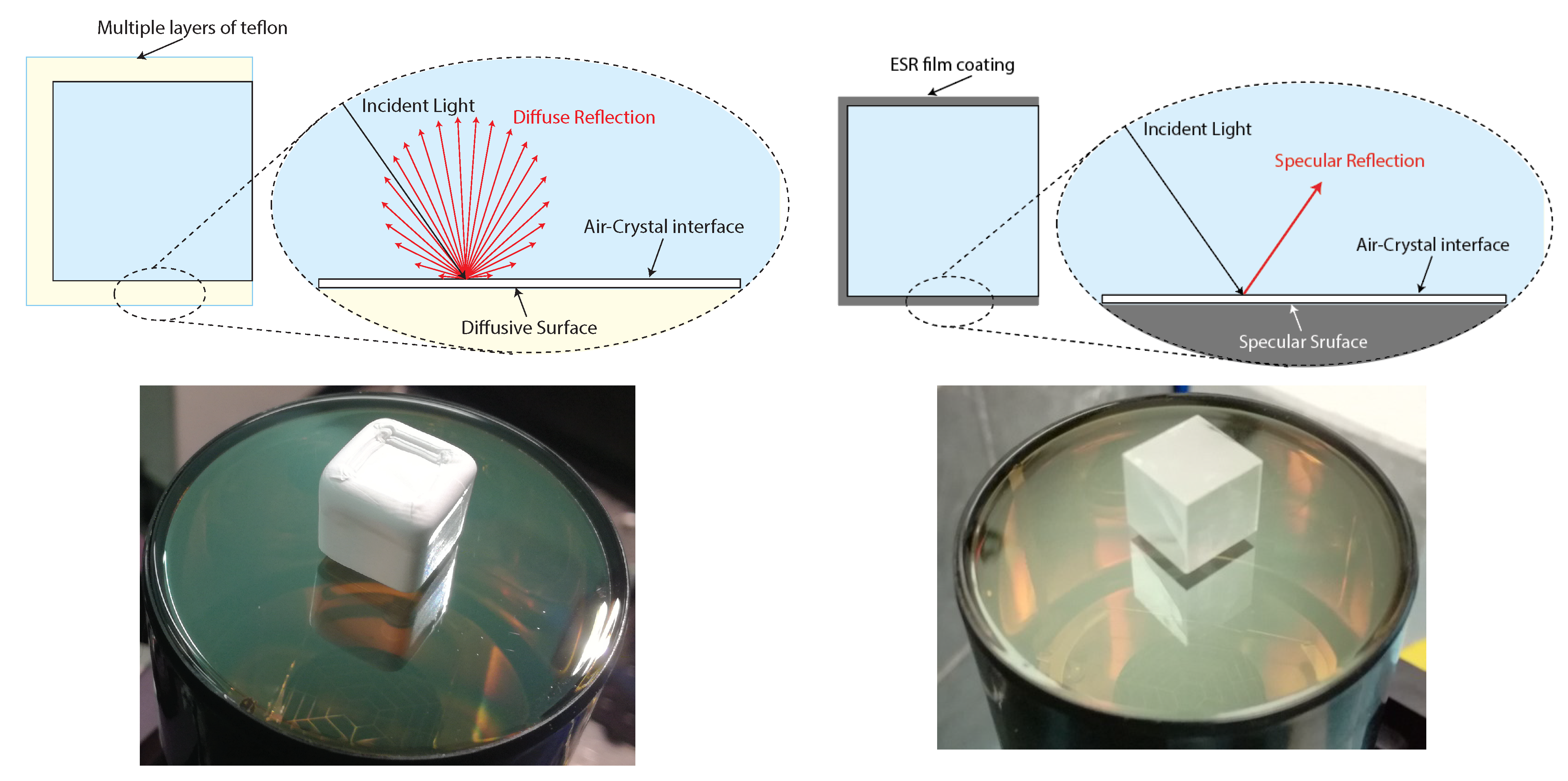
3.1. Coating Fabrication

In this work, PhCs were produced by Nanoimprint Lithography (Figure 7 Left). The patterns are reproduced on a resist using “soft stamps”, replicated from master molds made by different lithography techniques, such as e-beam, photo, laser interference, or colloidal lithography. In the present case, the master mold was made by colloidal lithography followed by Reactive Ion Etching (RIE) [33]. The soft stamp is then placed in contact with the resist and put under pressure. The nano-imprint process was used here with a TiO 2 sol-gel resist, which was deposited by spincoating at 5500 rpm on the scintillator surface before being patterned via nanoimprint [34,35,36,37,38]. The patterned layer is then annealed at a temperature optimized to match the required height and refractive index (n = 2.15). The pattern has a periodicity of 1000 nm and features cones of 560 nm in height and 300 nm in basal diameter as shown in Figure 8. The pattern has been encapsulated in a layer of silica sol-gel with refractive index of 1.46, matching that of the used optical grease. The hybrid organic/inorganic encapsulation layer was deposited via spray coating using an air brush spray gun with a 0.5-mm nozzle. The coating was first dried at room temperature, then annealed at 150 °C during 30 min to ensure its mechanical properties. This encapsulation procedure also allows to avoid the formation of air gaps, which could compromise the overall optical performance, between the bottom of the patterns and the grease if the latter was applied directly on top of the PhC. A schematic view of the implemented structure has already been shown in Figure 5. Modifications can be introduced, if required, to the pitch of the periodic structures as well as their shapes. This allows structural optimizations, which can be combined with different refractive index materials and wavelength ranges tuned to the applications at hand.
Two different DBR structures were implemented in this work (Figure 9). The first structure is shown on the left of Figure 9 and consists of a conventional mirror fabricated with an alternation of 13 layer pairs of S i O 2 and S i N x (81.2 nm and 60.9 nm in thickness respectively, for a central wavelength of 475 nm). This mirror was designed to align its reflectivity spectrum with the emission spectrum of the BGO crystal [30,40]. This coating was fabricated by means of a Plasma-enhanced Chemical Vapor Deposition (PECVD) process on a glass substrate. The reflectivity of this mirror was measured for several samples to validate the uniformity and reproducibility. All samples showed a very similar behavior, which is also in agreement with the simulation results. The simulations were performed using a custom Python routing based on the CAMFr (Cavity Modeling Framework) [41] libraries. The second mirror, shown on the right of Figure 9, was designed using an alternation of T a 2 O 5 and S i O 2 layers (61 nm and 39 nm in thickness respectively, for a central wavelength of 360 nm). The design of this mirror aimed at extending the reflectivity also in the region where conventional reflectors (e.g., ESR) start to be lossy [42]. Another motivation for this choice is that several inorganic scintillators, such as LYSO:Ce, show an emission spectrum shifted toward the blue [40]. The design center wavelength was thus selected to be 360 nm and the reflectivity spectrum of such a DBR is shown in Figure 9, right (blue line). This NUV-DBR, when coupled to a silver mirror, creates an enhanced reflective surface that ranges from 330 nm all the way to the infrared with a reflectivity in excess of 90% (Figure 9, right, green line). In this case as well, the mirror has been fabricated on a glass substrate but using RF sputtering (Alliance-Concept DP650) and characterized by mean of a spectroscopic reflectometer.

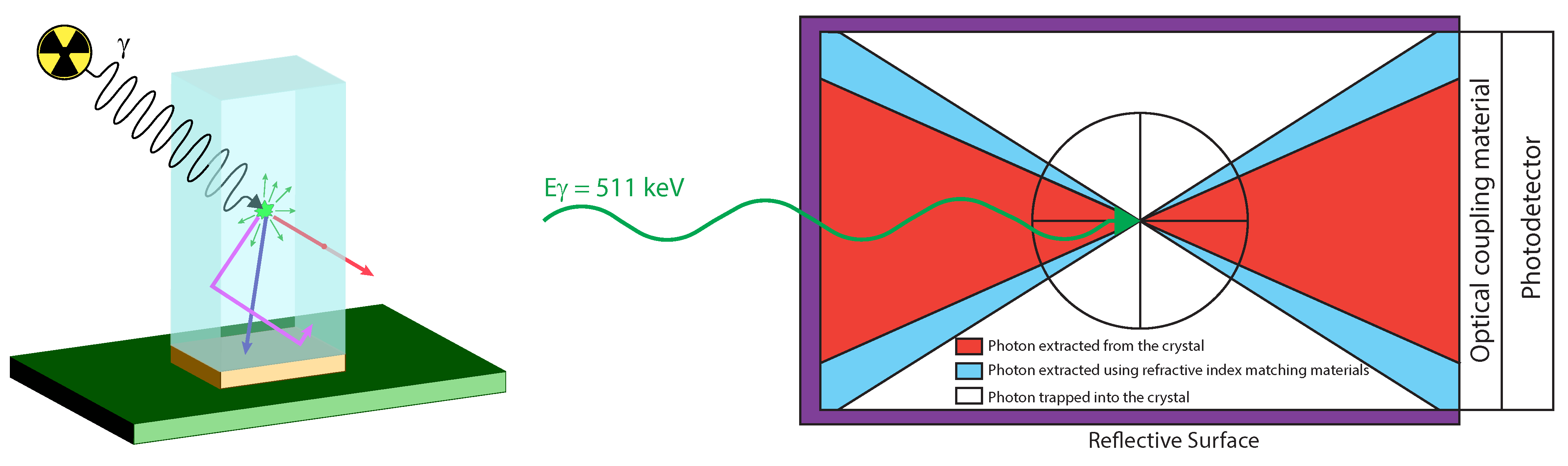
3.2. Experimental Setup

A set of ten 10 × 10 × 10 mm 3 crystal samples (Epic-Crystal) with polished surfaces was used. The scintillator was coupled in all cases to the photodetector using optical grease. A bare crystal without any coating represented the simplest configuration (ID = 1). Two additional configurations relied on the addition of ESR or Teflon applied to the side walls (ID = 3 and ID = 4), whereas in one further case a DBR was applied to the top surface only (ID = 2). Three configurations employed a PhC on a bare crystal (ID = 5), as well as together with Teflon wrapping on all sides or in combination with a DBR (ID = 6 and ID = 7), again only on the top surface. The DBRs used for the crystals are those shown in Figure 9, the left one for BGO and the right one for LYSO. The DBRs, deposited on glass substrates, were air-coupled in both cases. For each experiment, a crystal was placed with the exit surface coupled to a PMT (ET Enterprises Electron Tubes 9266KB) with optical grease ( n = 1.4 ), to measure the output light yield. The choice of a PMT was motivated by its high linearity with respect to the detected light, ease of use, and measurement reproducibility; the latter was also enhanced by the use of a micropositioner to control the optical glue layer down to a thickness of around 100 μ m. Each sample was irradiated with a gamma source ( 22 Na) of 4 MBq to induce scintillation inside the material. The output signal from the PMT was injected in an Ortec Digibase MCA, which provided the (uncalibrated) energy spectrum.
Each sample was tested for all the configurations before and after the implementation of the PhC on the output surface to verify the relative performance improvement. In addition, all the crystals were taken from the same batch and measured in the standard configuration. This procedure was needed to avoid evaluation errors due to possible light yield variations between crystals (especially from different batches) and to ensure that the PhC fabrication process did neither damage the crystals nor affect their performance.
The measurement was performed by coupling the crystal sample to the PMT inside a light tight box to avoid background noise given by environment light. The radioactive source was then placed on a custom-designed stand to keep a constant distance from the sample. The MCA was used to read the PMT photocurrent pulses, digitize them, and create a histogram. The measurement was performed for enough time, typically a few minutes, to allow the accumulation of a sufficiently high count number in the energy spectrum histogram and reduce the errors in the statistical analysis to a negligible level.

3.3. Data Analysis

The data acquired with the MCA was analyzed with a custom software in order to extract the energy resolution value and the number of ADC channels corresponding to the 511 keV and 1275 keV photopeaks. The spectrum was calibrated by utilizing the two 22 Na photopeaks. The final energy resolution was evaluated on the calibrated spectrum as the FWHM at the first photopeak, calculated using a Gaussian fit, divided by 511 keV. This value is independent of different systematic errors and variations between different samples of the same material. The comparison of the (calibrated) energy spectra resulting from different configurations did then allow us to measure the performance of each configuration in terms of variability, light gain, and energy resolution.

4. Results

The results obtained with the setup described in the previous section are summarized in Table 1. The table shows the measured light gain and energy resolution gain for seven crystal configurations, for both BGO and LYSO, taking as reference a standard configuration featuring a bare crystal wrapped in Teflon coupled with optical grease (ID = 4).
The use of a PhC pattern (Figure 8) showed a light extraction improvement of ∼41% and ∼10% for BGO and LYSO respectively, measured with respect to the best configuration without PhC (i.e., Teflon wrapping and optical grease). Concerning the corresponding energy resolution, the improvement was of ∼21% for BGO and ∼4% for LYSO. Figure 10 shows the energy spectra obtained using BGO (Top row) and LYSO (Bottom row) crystals; the use of a PhC did clearly improve in a significant way the overall amount of light in output of the scintillator. Moreover, a closer look at the BGO Sample 2 (Figure 10, Top left) curve illustrates how the spectrum becomes more detailed (the K-shell peak starts to be visible), indicating as well an improvement in energy resolution.
The use of the previously described DBRs on the top surface of a bare crystal showed a modest improvement compatible with what was previously reported in [30]. This is mostly due to the light that escapes from the lateral surfaces and will be discussed in more detail in the next section. Conventional solutions based on ESR or Teflon (3rd and 4th configurations in Table 1) featured quite similar performance and in line with expectations.
The silica sol-gel structure was extensively tested: It featured a resistance to cracking on bending higher than 1 T; an impact resistance of 18 J; a surface pencil hardness larger than 2 H, and an abrasion resistance (ISO3160) with no modification after 6 h (EN 13523).

5. Discussion

The most important result achieved by this study was the significant light extraction enhancement when a modified nanoimprinted photonic crystal, enhanced with a sol-gel protection (hybrid organic/inorganic silica sol-gel buffer layer) to increase its robustness, was applied on the output surface of an inorganic scintillator. The best result was obtained by encapsulating the crystal with reflectors (e.g., Teflon) on the side surfaces to redirect the light toward the output. The PhC efficiency clearly improved with the growing scintillator refractive index. A quite substantial improvement in the performance of BGO has indeed been obtained, whereas its use on LYSO crystals showed a milder gain. This is not surprising per se, given the large difference of refractive index between the two scintillators (2.15 for BGO vs. 1.8 for LYSO), and the fact that the simple use of a refractive index matching material is already providing good optical coupling for LYSO. This explanation is also accredited by similar performance trends for both LYSO and BGO in experiments featuring PhCs deposited on crystals which are air-coupled to photodetectors. Indeed, from measurements performed on our air-coupled samples with Teflon wrapping we observed an improvement of ∼25% and ∼15% in energy resolution and ∼50% and ∼30% in light gain for LYSO and BGO, respectively. In this case, the gain provided by the PhC coating, without employing optical coupling compounds, was in line with what reported in the literature [17,18,19,20,21,22,26].
Concerning the use of DBR mirrors, only a modest result (in particular considering the energy resolution) was obtained when using a single mirror applied on the top surface of the two kinds of crystals. This is mainly due to the fact that in this configuration (2nd in Table 1), the lateral surfaces of the crystal are uncovered, and a significant part of the scintillation light gets lost. The light gain does slightly increase when air-coupling the mirrors on five of the six surfaces, although it is still below our expectations. The main reasons lies in the technological hurdles which need to be overcome for the direct deposition of the reflective coating on the surface of the scintillators. The corresponding process is indeed quite complex, suffering from edge effects or generating a sufficient amount of heat to compromise the crystals’ performance. As a result, the performance of the coating (especially DBRs) changes close to the edges of the sample. Moreover, we observed a degradation of performance when a plasma-based process was used; the underlying reasons are currently being investigated.

6. Conclusions and Outlook

Different light extraction enhancement techniques for two inorganic scintillators (LYSO and BGO) were analyzed and compared. While LYSO still represents the scintillator of reference in PET applications, we chose to investigate BGO as well due to renewed interest, mostly thanks to its small but prompt Cherenkov emission component as well as lower cost. Novel approaches using thin film coatings and nanoimprinted nanostructures (PhCs) were proposed (Figure 5) and characterized by means of a set of 1 cm 3 cubic crystal samples coupled with grease to the window of a PMT. Each sample was irradiated with a gamma source and tested for all the configurations before and after the implementation of the PhC. Concerning the PhC, we added a silica buffer layer which encapsulates the nanostructures, thereby ensuring structural robustness and optimal coupling to the photodetector optical window, contrary to most previous air-coupled implementations, while ensuring unvaried PhC performance. The use of the PhC on the output surface showed a significant improvement in light extraction and energy resolution (see Table 1), in particular for BGO. This could possibly lead to reconsider the use of this scintillator in the development of future TOF-PET modules.
In addition to the core work on improved photonic crystals, we did also investigate the use of thin film coatings. Such reflective very thin structures (order of 1 μ m), once applied to the sides of the scintillators, can allow a significant reduction of the dead space between crystals, and a corresponding improvement of the packing fraction (which in turn translates into an improvement of the overall detection efficiency of the system). This is of particular relevance when implementing tiles of miniaturized (sub-millimiter) crystal needles where the thickness of the crystal coating has a high impact, and can also contribute to suppression of optical crosstalk between neighboring needles. Several DBRs were simulated prior to fabrication and two different structures compared, both deposited on a glass substrate. One structure was optimized for BGO and another, whose reflectivity extended to the NUV, was coupled to a silver mirror, resulting in a combined very broad reflectivity range. Other wavelength ranges can be implemented if needed, thereby exploiting the full tunability potential of DBRs. The measured reflectivity spectra of the aforementioned DBRs agreed well with the simulated data, but the experimental results obtained when using them air-coupled to the crystals were somewhat below expectations. This was mostly due to several technological hurdles which still need to be overcome for the direct deposition of the reflective coating on the surface of the scintillators, and which we are currently exploring, together with the direct deposition of metal films.
We did indeed investigate the possibility of directly depositing metals on the crystal surface, either by metal evaporation, or by Physical Vapor Deposition (PVD). The former works at room temperature, i.e., without involving a plasma entering in contact with the crystal surface, and was implemented with success for the deposition of silver, although we encountered adhesion issues. The latter was tested with aluminum, resulting in no apparent damage to the surface of the crystal, with an adhesion better than the one of silver, also without resorting to adhesion layers. The study of these additional treatments is still under development.
The next steps concerning the PhC will consist in extending the experimental characterization to crystal needles as well as measuring the possible impact of the PhC on the spatial reconstruction on one side, and the temporal on the other in terms of timing performance. We expect an improvement of CRT as also suggested in [18,21,43,44]. Another interesting, though challenging perspective is represented by the simulation of the light interaction with the entire scintillator-photodetector interface and the scintillating crystal itself, to optimize the output gain. This will require various simulation tools and more specifically, multiscale modeling. Such tools are currently available and will be tested in the near future [45].

Author Contributions

Conceptualization, F.G., N.D., C.B.; methodology, F.G., E.R., E.V., C.B.; software, E.R.; validation, F.G., E.R.; data analysis, E.R.; investigation, F.G., E.R., V.G., S.F.; optical simulations, S.F., N.D.; sample fabrication, H.K., V.G., D.T., S.F., N.D.; setup implementation, F.G., E.R., E.V.; sample characterization, F.G., E.R., S.F.; data curation, E.R.; writing—original draft preparation, F.G., E.R., S.F.; writing—review and editing, F.G., E.R., S.F., D.T., E.C., C.B.; visualization, F.G., E.R., S.F.; supervision, D.T., E.C., C.B.; funding acquisition, E.C., C.B. All authors have read and agreed to the published version of the manuscript.

Funding

This research was supported, in part, by the Swiss National Science Foundation under grant 200021-169465 and Sinergia CRSII5-177165.

Institutional Review Board Statement

Not applicable.

Informed Consent Statement

Not applicable.

Data Availability Statement

Not applicable.

Acknowledgments

The authors would like to thank Loic Le Cunff and Gilles Lerondel for fruitful discussions and for suggesting the use of self-assembled structures for light extraction. H.K. would also like to acknowledge the use of the Nano’mat platform and the guidance of Gilles Lerondel for the fabrication of the silicon mold using colloidal self-assembly combined with dry etching techniques. EPFL also gratefully acknowledges the generous support of the Swiss National Science Foundation and of EPFL’s CMi (Center of MicroNanoTechnology) staff.

Conflicts of Interest

The authors declare no conflict of interest.

References

  1. Gundacker, F.A.S. Understanding and simulating SiPMs. Nucl. Instrum. Methods Phys. Res. Sect. A Accel. Spectrometers Detect. Assoc. Equip. 2019, 16–35. [Google Scholar] [CrossRef]
  2. Gundacker, S.; Heering, A. The silicon photomultiplier: Fundamentals and applications of a modern solid-state photon detector. Phys. Med. Biol. 2020, 65, 17TR01. [Google Scholar] [CrossRef]
  3. Mao, R.; Zhang, L.; Zhu, R. Optical and Scintillation Properties of Inorganic Scintillators in High Energy Physics. IEEE Trans. Nucl. Sci. 2008, 55, 2425–2431. [Google Scholar] [CrossRef] [Green Version]
  4. Mao, R.; Zhang, L.; Zhu, R. Crystals for the HHCAL Detector Concept. IEEE Trans. Nucl. Sci. 2012, 59, 2229–2236. [Google Scholar] [CrossRef] [Green Version]
  5. Wieczorek, H.; Thon, A.; Dey, T.; Khanin, V.; Rodnyi, P. Analytical model of coincidence resolving time in TOF-PET. Phys. Med. Biol. 2016, 61, 4699–4710. [Google Scholar] [CrossRef] [PubMed]
  6. Vinogradov, S. Approximations of coincidence time resolution models of scintillator detectors with leading edge discriminator. Nucl. Instrum. Methods Phys. Res. Sect. A Accel. Spectrometers Detect. Assoc. Equip. 2018, 149–153. [Google Scholar] [CrossRef]
  7. Lerondel, G.; Le Cunff, L.; Montiel, R.S.; Lecoq, P.; Turover, D.; Grosso, D. Method for Optimizing the Collection of Photons in Scintillator Crystals, and Related Crystal and Uses. Patent Application Number: WIPO (PCT) WO2015136165A1, 17 September 2015. [Google Scholar]
  8. Brunner, S.E.; Schaart, D.R. BGO as a hybrid scintillator/Cherenkov radiator for cost-effective time-of-flight PET. Phys. Med. Biol. 2017, 62, 4421–4439. [Google Scholar] [CrossRef]
  9. Janecek, M. Reflectivity Spectra for Commonly Used Reflectors. IEEE Trans. Nucl. Sci. 2012, 59, 490–497. [Google Scholar] [CrossRef] [Green Version]
  10. Ghosh, S.; Haefner, J.; Martín-Albo, J.; Guenette, R.; Li, X.; Villalpando, A.L.; Burch, C.; Adams, C.; Álvarez, V.; Arazi, L.; et al. Dependence of polytetrafluoroethylene reflectance on thickness at visible and ultraviolet wavelengths in air. J. Instrum. 2020, 15, P11031. [Google Scholar] [CrossRef]
  11. ter Weele, D.N.; Schaart, D.R.; Dorenbos, P. Picosecond Time Resolved Studies of Photon Transport Inside Scintillators. IEEE Trans. Nucl. Sci. 2015, 62, 1961–1971. [Google Scholar] [CrossRef]
  12. Yang, F.; Hu, C.; Zhang, L.; Zhu, R.Y. UV–Visible reflectance of common light reflectors and their degradation after an ionization dose up to 100 Mrad. Nucl. Instrum. Methods Phys. Res. Sect. A Accel. Spectrometers Detect. Assoc. Equip. 2021, 992, 165043. [Google Scholar] [CrossRef]
  13. Kuntner, C.; Stout, D. Quantitative preclinical PET imaging: Opportunities and challenges. Front. Phys. 2013, 2. [Google Scholar] [CrossRef] [Green Version]
  14. 3M. Enhanced Specular Reflector (ESR). 2019. Available online: http://multimedia.3m.com/mws/media/374730O/vikuiti-tm-esr-sales-literature.pdf?fn=ESR%20ss2.pdf (accessed on 17 October 2019).
  15. Loignon-Houle, F.; Pepin, C.M.; Charlebois, S.A.; Lecomte, R. Reflectivity quenching of ESR multilayer polymer film reflector in optically bonded scintillator arrays. Nucl. Instrum. Methods Phys. Res. Sect. A Accel. Spectrometers Detect. Assoc. Equip. 2017, 62–67. [Google Scholar] [CrossRef]
  16. Knapitsch, A.R. Photonic Crystals: Enhancing the Light Output of Scintillation Based Detectors. Ph.D. Thesis, Vienna University Technology, Atominst, Vienna, Austria, 2012. [Google Scholar]
  17. Knapitsch, A.; Lecoq, P. Review on photonic crystal coatings for scintillators. Int. J. Mod. Phys. A 2014, 29, 1430070. [Google Scholar] [CrossRef]
  18. Salomoni, M.; Pots, R.; Auffray, E.; Lecoq, P. Enhancing Light Extraction of Inorganic Scintillators Using Photonic Crystals. Crystals 2018, 8, 78. [Google Scholar] [CrossRef] [Green Version]
  19. Chen, C.; Zhu, Z.; Liu, B.; Cheng, C.; Chen, H.; Gu, M.; Liu, J.; Chen, L.; Ouyang, X. Effect of a conformal layer on the photonic crystal for light extraction of scintillator. Nucl. Instrum. Methods Phys. Res. Sect. A Accel. Spectrometers Detect. Assoc. Equip. 2020, 162953. [Google Scholar] [CrossRef]
  20. Liu, F.; Yang, Y.; Liu, Y.; Tang, W.; Zhu, J.; Wang, P.; Ouyang, X.; Zhao, N.; Qi, F.; Wang, H.; et al. Large energy resolution improvement of LYSO scintillator by electron beam lithography method. AIP Adv. 2020. [Google Scholar] [CrossRef]
  21. Pots, R.; Salomoni, M.; Gundacker, S.; Zanettini, S.; Gâté, V.; Usureau, E.; Turover, D.; Lecoq, P.; Auffray, E. Improving light output and coincidence time resolution of scintillating crystals using nanoimprinted photonic crystal slabs. Nucl. Instrum. Methods Phys. Res. Sect. A Accel. Spectrometers Detect. Assoc. Equip. 2019, 940. [Google Scholar] [CrossRef]
  22. Zhu, Z.; Liu, B.; Zhang, H.; Ren, W.; Cheng, C.; Wu, S.; Gu, M.; Chen, H. Improvement of light extraction of LYSO scintillator by using a combination of self-assembly of nanospheres and atomic layer deposition. Opt. Express 2015, 23, 7085–7093. [Google Scholar] [CrossRef]
  23. Singh, B.; Marshall, M.S.J.; Waterman, S.; Pina-Hernandez, C.; Koshelev, A.; Munechika, K.; Knapitsch, A.; Salomoni, M.; Pots, R.; Lecoq, P.; et al. Enhanced Scintillation Light Extraction Using Nanoimprinted Photonic Crystals. IEEE Trans. Nucl. Sci. 2018, 65, 1059–1065. [Google Scholar] [CrossRef]
  24. Xiao, O.; Liu, B.; Xiang, X.; Chen, L.; Xu, M.; Song, X.; Li, Y. Enhanced light output of CsI(Na) scintillators by photonic crystals. Nucl. Instrum. Methods Phys. Res. Sect. A Accel. Spectrometers Detect. Assoc. Equip. 2020, 164007. [Google Scholar] [CrossRef]
  25. Xiao, O.; Liu, B.; Xiang, X.; Zhu, Z.; Chen, L.; Song, X.; Yuan, D.; Chen, C. Enhancement of the energy resolution of CsI(Na) scintillators by photonic crystals prepared with dry-transfer technique. Opt. Express 2020, 28, 33077–33083. [Google Scholar] [CrossRef]
  26. Liu, Y.; Liu, F.; Tang, W.; Yang, Y.; Zhu, J.; Zhao, N.; Qi, F.; Xiao, O. Light extraction enhancement of BGO scintillator by monolayers of SiO2 periodic array. AIP Adv. 2019. [Google Scholar] [CrossRef] [Green Version]
  27. Gramuglia, F.; Lee, M.; Venialgo, E.; Bruschini, C.; Charbon, E. Towards 10 ps SPTR and Ultra-Low DCR in SiPMs Through the Combination of Microlenses and Photonic Crystals. In Proceedings of the 2017 IEEE Nuclear Science Symposium and Medical Imaging Conference (NSS/MIC), Atlanta, GA, USA, 21–28 October 2017; pp. 1–3. [Google Scholar] [CrossRef]
  28. Sun, Q.; Peng, Q.; Wu, Z.; Huang, Q.; Xu, J. Ultra-thin high-reflector film designed for LYSO scintillators. In Proceedings of the 2016 IEEE Nuclear Science Symposium, Medical Imaging Conference and Room-Temperature Semiconductor Detector Workshop (NSS/MIC/RTSD), Strasbourg, France, 29 October–6 November 2016; pp. 1–2. [Google Scholar] [CrossRef]
  29. Sun, Q.; Peng, Q.; Wu, Z.; Xie, S.; Huang, Q.; Xu, J. Design of ultra-thin anti-reflection films directly coated on LYSO scintillators. In Proceedings of the 2017 IEEE Nuclear Science Symposium and Medical Imaging Conference (NSS/MIC), Atlanta, GA, USA, 21–28 October 2017; pp. 1–3. [Google Scholar] [CrossRef]
  30. Gramuglia, F.; Descharmes, N.; Venialgo, E.; Herzig, H.P.; Charbon, E.; Bruschini, C. Light Extraction Enhancement in Scintillation Crystals Using Thin Film Coatings. In Proceedings of the 2018 IEEE Nuclear Science Symposium and Medical Imaging Conference Proceedings (NSS/MIC), Sydney, Australia, 10–17 November 2018; pp. 1–2. [Google Scholar] [CrossRef]
  31. Aliofkhazraei, M. Advances in Nanostructured Composites: Volume 1: Carbon Nanotube and Graphene Composites; CRC Press: Boca Raton, FL, USA, 2019. [Google Scholar]
  32. Fink, Y.; Winn, J.N.; Fan, S.; Chen, C.; Michel, J.; Joannopoulos, J.D.; Thomas, E.L. A Dielectric Omnidirectional Reflector. Science 1998, 282, 1679–1682. [Google Scholar] [CrossRef] [Green Version]
  33. Kadiri, H.; Kostcheev, S.; Turover, D.; Salas-Montiel, R.; Nomenyo, K.; Gokarna, A.; Lerondel, G. Topology assisted self-organization of colloidal nanoparticles: Application to 2D large-scale nanomastering. Beilstein J. Nanotechnol. 2014, 5, 1203–1209. [Google Scholar] [CrossRef]
  34. Zanchetta, E.; Auzelyte, V.; Brugger, J.; Savegnago, A.; Della Giustina, G.; Brusatin, G. Highly inorganic titania based solgel as directly patternable resist for micro- and nano- structured surfaces. Microelectron. Eng. 2012, 98, 176–179. [Google Scholar] [CrossRef]
  35. Ganesan, R.; Dumond, J.; Saifullah, M.S.M.; Lim, S.H.; Hussain, H.; Low, H.Y. Direct Patterning of TiO2 Using Step-and-Flash Imprint Lithography. ACS Nano 2012, 6, 1494–1502. [Google Scholar] [CrossRef]
  36. Ma, P.; Xu, Z.; Wang, M.; Lu, L.; Yin, M.; Chen, X.; Li, D.; Ren, W. Fast fabrication of TiO2 hard stamps for nanoimprint lithography. Mater. Res. Bull. 2017, 90, 253–259. [Google Scholar] [CrossRef]
  37. Yoon, K.; Yang, K.Y.; Lee, H. Fabrication of polycrystalline TiO2 nanopatterns by TiO2 sol base imprint lithography. Thin Solid Film. 2009, 518, 126–129. [Google Scholar] [CrossRef]
  38. Yoon, K.M.; Yang, K.Y.; Lee, H.; Kim, H.S. Formation of TiO2 nanopattern using reverse imprinting and sol-gel method. J. Vac. Sci. Technol. B Microelectron. Nanometer Struct. Process. Meas. Phenom. 2009, 27, 2810–2813. [Google Scholar] [CrossRef]
  39. Zanettini, S.; Gâté, V.; Usureau, E.; Ruscica, J.; Hamouda, F.; Nomenyo, K.; Le Cunff, L.; Kadiri, H.; Lerondel, G.; Salomoni, M.; et al. Improved Light Extraction Efficiency on 2 inches LYSO with Nanopatterned TiO2 Photonic Crystals. IEEE Strasbg. 2016. [Google Scholar]
  40. Valais, I.; Michail, C.; David, S.; Nomicos, C.; Panayiotakis, G.; Kandarakis, I. A comparative study of the luminescence properties of LYSO:Ce, LSO:Ce, GSO:Ce and BGO single crystal scintillators for use in medical X-ray imaging. Phys. Medica 2008, 24, 122–125. [Google Scholar] [CrossRef] [PubMed]
  41. Bienstman, P. Rigorous and Efficient Modelling of Wavelenght Scale Photonic Components. Ph.D. Thesis, Ghent University, Ghent, Belgium, 2001. [Google Scholar]
  42. Yang, G.; Huang, H.; Wang, H. High-reflectance of hybrid reflector with distributed Bragg reflector and metal mirror for flip-chip ultra-violet light-emitting diodes. In Proceedings of the SPIE 9295, International Symposium on Optoelectronic Technology and Application 2014: Laser Materials Processing; and Micro/Nano Technologies, Beijing, China, 18 December 2014; Jin, G., Zhuang, S., Liu, J., Eds.; International Society for Optics and Photonics: Bellingham, WA, USA, 2014; Volume 9295, pp. 54–59. [Google Scholar] [CrossRef]
  43. Lecoq, P.; Auffray, E.; Knapitsch, A. How Photonic Crystals Can Improve the Timing Resolution of Scintillators. IEEE Trans. Nucl. Sci. 2013, 60, 1653–1657. [Google Scholar] [CrossRef] [Green Version]
  44. Iltis, A.; Zanettini, S.; de Magalhaes, L.; Tata, C.; Soledade, A.; Hmissi, M.; Khadiri, H.; Gaté, V.; Turover, D. Impact on timing and light extraction of a photonic crystal as measured on a half patterned LYSO crystal: Implications for time of flight PET imaging. J. Instrum. 2019, 14, P06036. [Google Scholar] [CrossRef]
  45. Castro, C.S.; Cunff, L.L.; Vial, A.; Lerondel, G. Light management in scintillator crystals: A multi-scale computational study. In UV and Higher Energy Photonics: From Materials to Applications 2018; Lérondel, G., Kawata, S., Cho, Y.H., Eds.; International Society for Optics and Photonics: Bellingham, WA, USA, 2018; Volume 10727. [Google Scholar] [CrossRef]
Figure 1. Main sources of light losses at the scintillator (light blue)-photodetector (D) interface: (a) Light collection efficiency ( L 2 , with L being the distance between the light source and the photodector); (b) total internal reflection ( T I R a n g l e = s i n ( n c r y s t a l / n a i r )); and (c) Fresnel losses ( Δ ( n ) 2 ).
Crystals 11 00362 g001
Figure 2. Simplified ionizing radiation detection scheme. (Left) The scintillator, attached to a photodetector, is irradiated with gamma rays. The interaction between the ionizing particles and the crystal structure generates optical photons isotropically. The latter can reach directly the output surface and be extracted from the crystal (blue arrow). Some photons will however be refracted at the other crystal surfaces and eventually escape from the crystal (red arrow). Other photons will undergo total internal reflection and be trapped within the crystal (purple arrow). (Right) Only a limited portion of photons is going to be extracted when employing specular reflective surfaces (violet structures). The situation improves by optimizing the optical coupling.
Crystals 11 00362 g002
Figure 3. Typical scintillator wrapping examples. (Left): Teflon (diffusive) wrapping vs. (Right): ESR (specular) wrapping. (Top row): Schematic representation, (Bottom row): Actual crystals attached to the window of a Photomultiplier Tube (PMT).
Crystals 11 00362 g003
Figure 4. Coating thickness impact on the packing fraction. The coating thickness becomes non-negligible when reducing the crystal size (L), thus affecting the overall efficiency of the system.
Crystals 11 00362 g004
Figure 5. Proposed photonic crystal solution: The scintillator is covered by reflective material and the novel Photonic Crystal (PhC) structure is implemented on the output surface. The PhC is composed of titanium oxide nanocones surrounded by a buffer layer of silicon oxide with a refractive index of about 1.4. The solution allows a stable coupling with the photodetector by means of a refractive index matching material, such as grease.
Crystals 11 00362 g005
Figure 6. Distributed Bragg Reflector (DBR) scheme. Left: Schematic overview. The DBR structure is composed of a periodic alternation of layers with different index of refraction ( n H and n L ). The number of layers and the difference in refractive index between the layers have an impact on the mirror performance. Right: SEM cross-section of a DBR implemented in the EPFL’s clean rooms at the Center of MicroNanotechnology (CMI). The layer stack is clearly visible. Scale bar: 200 nm.
Crystals 11 00362 g006
Figure 7. Simplified nanoimprinting process steps for pattern implementation (left) (for details see text). Atomic Force Microscope (AFM) image of a small area of the implemented pattern (right) [39].
Crystals 11 00362 g007
Figure 8. SEM photonic crystal nanostructure images before the implementation of the buffer layer. Left: Top view (scale bar: 200 nm), Right: Side view (scale bar: 2000 nm).
Crystals 11 00362 g008
Figure 9. Reflectivity spectra of the DBRs implemented on glass substrates. Left: A conventional DBR designed with a center wavelength of 480 nm, to match the emission spectrum of BGO. Right: A combination of DBR (centered at 360 nm) and silver coating to extend the spectrum toward the red. Top row, left: Simulation results vs. measurements of different samples, Top row, right: Measurement results of the complete structure as well as its components. Bottom row: Schematic representation of the respective DBR architectures.
Crystals 11 00362 g009
Figure 10. (Top row, left): Examples of energy spectra obtained with BGO samples in different configurations. Ref1: Reference crystal with Teflon wrapping, air-coupled; Sample 1: Crystal wrapped with Teflon with PhC on the output surface, air-coupled; Ref 2: Reference crystal with Teflon wrapping and optical grease; Sample 2: Crystal with Teflon wrapping, PhC on the output surface and optical grease. (Top row, right): Corresponding calibration curves derived from the position of the two photopeaks (511 keV and 1275 keV) to eliminate any offset. The slope of the curves provides a visualization of the light gain improvement. Bottom row: Same results for LYSO.
Crystals 11 00362 g010
Table 1. Summary of all experimental results on 10 × 10 × 10 mm 3 BGO and LYSO crystals in seven configurations. Reference: A standard configuration featuring a bare crystal wrapped in Teflon (ID = 4). The scintillator was coupled in all cases to the photodetector using optical grease. The light gain and the energy resolution have been calculated on the first peak of the spectrum (511 keV).
Comparison of Experimental Results
IDCrystalConfigurationLight GainEnergy Resolution (%)Energy Resolution Improvement
1BGOBare crystal & Opt. Grease0.5520.8 ± 0.480.74
2BGOBare crystal & Opt. Grease & DBR (top)0.6419.3 ± 0.260.80
3BGOESR & Opt. Grease0.9815.6 ± 0.290.99
4BGOTeflon & Opt. Grease1.0015.4 ± 0.191.00
5BGOPhC Pattern & Opt. Grease0.8017.2 ± 0.580.90
6BGOPhC Pattern, Teflon & Opt. Grease1.4112.7 ± 0.361.21
7BGOPhC Pattern & Opt. Grease & DBR (top)0.8816.4 ± 0.570.94
1LYSOBare crystal & Opt. Grease0.7412.2 ± 0.320.85
2LYSOBare crystal & Opt. Grease & DBR (top)0.7911.8 ± 0.360.88
3LYSOESR & Opt. Grease1.0010.4 ± 0.121.00
4LYSOTeflon & Opt. Grease1.0010.4 ± 0.151.00
5LYSOPhC Pattern & Opt. Grease0.8511.4 ± 0.330.91
6LYSOPhC Pattern, Teflon & Opt. Grease1.1010.0 ± 0.241.04
7LYSOPhC Pattern & Opt. Grease & DBR (top)0.8611.3 ± 0.340.92
Publisher’s Note: MDPI stays neutral with regard to jurisdictional claims in published maps and institutional affiliations.

