Article

Effects of Matrix Silicon Content on the Plasma Electrolytic Oxidation of Al-Si Alloys Using Different Power Modes

1
College of Materials Science and Technology, Dongguan University of Technology, Dongguan 523820, China
2
College of Materials Science and Technology, South China University of Technology, Guangzhou 510641, China
*
Author to whom correspondence should be addressed.
Submission received: 8 December 2021 / Revised: 28 December 2021 / Accepted: 13 January 2022 / Published: 17 January 2022
(This article belongs to the Special Issue Nanocrystalline Coating Alloy)

Abstract

:
The plasma electrolytic oxidation (PEO) of pure Al and Al alloys containing 4, 9, 12, or 15 wt.% Si were investigated under pulsed bipolar current and pulsed bipolar voltage modes, respectively. It was determined that the discharge sparks preferentially occurred on the SiO2 relative to the Al2O3 during the initial stage of PEO processing regardless of the power mode. Following 30 min of PEO treatment under the two modes, the thicknesses of the layers decreased, whereas their specific energy consumption increased with increasing Si content in the matrix. The presence of primary Si in the alloy with 15 wt.% Si had a significantly negative effect on the PEO process in the pulsed bipolar current mode: The layer thickness decreased by 45%, and its specific energy consumption increased by 52%, compared with those on pure Al. However, in the pulsed bipolar voltage mode, the layer thickness on the evaluated samples only decreased slightly, and it became much more similar after treatment.

Graphical Abstract

1. Introduction

Cast Al-Si alloys are commonly used to produce mechanical parts because of their excellent castability, low shrinkage, and high specific strength, among other beneficial features [1,2]. Some eutectic or near-eutectic Al-Si alloys (e.g., AlSi12, AlSi10Mg) have recently been considered as some of the most promising materials for the additive manufacturing of Al alloy products [3,4]. However, the low hardness and poor corrosion and abrasion resistance properties significantly limit the lifetime of Al-Si alloy products [5,6]. Therefore, surface technologies, such as anodizing [7], laser remelting [8], plasma electrolytic oxidation (PEO) [9], and cathode plasma electrolytic deposition [10] have been applied to address these issues.
In particular, PEO has been widely employed for the surface modification of Al, Mg, and Ti alloys because it is an eco-friendly and high-efficiency method [11,12]. It is an effective method for the surface modification of wrought, cast, or foamed Al alloys (e.g., 2024, 6063, 7075, A356), which are often used to fabricate mechanical, automobile, or electronic products [13,14,15,16]. Recently, PEO has attracted increasing interest in terms of fabricating in situ ceramic layers on Al-Si alloys that are used in the manufacture of pistons, wheels, and many other products because the PEO layer exhibits excellent adhesion, anti-wear, and corrosion performance and demonstrates significant advantages as an anodic film [9,17,18,19]. However, the eutectic or primary Si grains in the Al alloys have adverse impacts on the growth and structure of the PEO layer [20,21]. The mechanism governing Si particles had been discussed in some previous studies; for example, it was proposed that Si inhibited the growth of the film during the anodic oxidation stage [18,22]. The micro-arc discharges began at the Al-Si interfaces when the voltage reached a critical value, and then, the discharges gradually spread across the primary Al and Si regions [23]. The Al2O3 and SiO2 phases mixed together and converted to mullite under the high temperature conditions generated by the discharge sparks [23]. The layer on the bulk Si was much coarser during the early stage of oxidation, but the surface morphology of the layer became more uniform as the PEO process continued [21,23]. In addition, the layer thickness, density, and abrasion resistance all decreased as the Si content increased [21,24]. Several solutions have been implemented to mitigate the adverse impacts of Si or to improve the performance of the PEO layer on Al-Si alloys. For example, a pre-anodizing treatment of the A356 alloy accelerated the layer deposition rate and enhanced the energy efficiency of the PEO process [25]. The fine Si grains in the eutectic Al-Si alloy helped improve the compactness and corrosion resistance of the PEO layer [6,26]. The elimination of Si on the surface of Al-Si alloys reduced the mullite content and enhanced the corrosion resistance of the PEO layer [26,27]. To obtain a uniform oxide layer on the Al-Si alloy, additives such as NH4VO3 could be introduced [28]. Such aluminate-based electrolytes are known to promote the formation of a denser coating on cast Al-Si alloys [29]. In addition, a post-PEO sealing process improved the hydrophobicity, impedance, and anti-corrosion performance of the PEO layer on an A356 alloy [30]. Ceramic-based self-lubricating layers (i.e., PEO/PI/WS2) prepared via PEO and spin-layer methods significantly improved the tribological properties of a ZL109 alloy [31]. Nevertheless, the pre- or post-treatments mentioned above render the surface modification process relatively complex, thus making it undesirable for industrial applications.
The PEO process is very intricate owing to the involvement of thermal, chemical, electrochemical, and plasma reactions at the substrate-electrolyte interface [32]. In addition to the alloying elements and electrolyte composition aspects mentioned above [24,30], electrical parameters (e.g., power supply mode, applied voltage, current density, duty ratio, pulse frequency) are also critical factors in terms of the formation, morphology, and performance of the PEO layer on Al-Si alloys [18,33]. A constant current (–10 to 35 A/dm2) [22,23] or constant voltage (–140 to +550 V) [24,31] mode based on an asymmetric alternating current (AC) power supply is commonly applied for the PEO of Al-Si alloys. The oxidation process and layer characteristics change significantly under different power supply modes, although previous studies regarding the evolution of Si grains during the initial stage of PEO treatment were mostly based on a constant-current mode. Therefore, in this work, pure Al and Al-Si binary alloys with different Si contents were treated by PEO with pulsed bipolar current (PBC) and pulsed bipolar voltage (PBV) modes. The effects of the Si content on the layer growth process, characteristics, and energy efficiency were analyzed under different power modes.

2. Materials and Methods

Pure Al (>99.7%) and cast Al-Si binary alloys with Si contents corresponding to 5, 9, 12, and 15 wt.% were obtained from commercial sources and used as the substrate material; the Al-Si alloys were labeled as Al-5Si, Al-9Si, Al-12Si, and Al-15Si, respectively. The size of each sample was 20 mm × 20 mm × 4 mm, and they were polished using 1200-grit sandpaper, cleaned via ultrasonic treatment in acetone, and then dried under hot air before the PEO treatment.
The electrolyte was comprised 10 g/L of Na2SiO3, 2 g/L of NaOH, and 5 g/L of C6H12N4. The PEO layers were prepared on the samples using an AC pulsed power supply (WHD60, Harbin, China) with a maximum power of 60 kW. A schematic diagram of the output current and voltage signals is presented in Figure 1. When using the PBC mode, the applied positive current density was 10 A·dm−2, and the negative current density was 4 A·dm−2. When applying the PBV mode, the positive voltage was 450 V, and the negative voltage was 50 V. The pulse frequency was 400 Hz, and the duty cycle was 25% in both power modes.
The thickness of each PEO layer was measured using an eddy current thickness gauge (Surfix N, PHYNIX Sensortechnik GmbH, Neuss, Germany). The morphology and elemental composition were analyzed with a field emission scanning electron microscope (Nova NanoSEM 430, Fei Company, Hillsboro, OR, USA) equipped with an energy dispersive spectrometer (EDS INCA, Oxford Instruments, High Wycombe, UK). The crystalline structures of coated samples were characterized via X-ray diffraction (Miniflex 600, Rigaku, Tokyo, Japan) using Cu Kα radiation over a 2θ range of 20–70°.

3. Results and Discussion

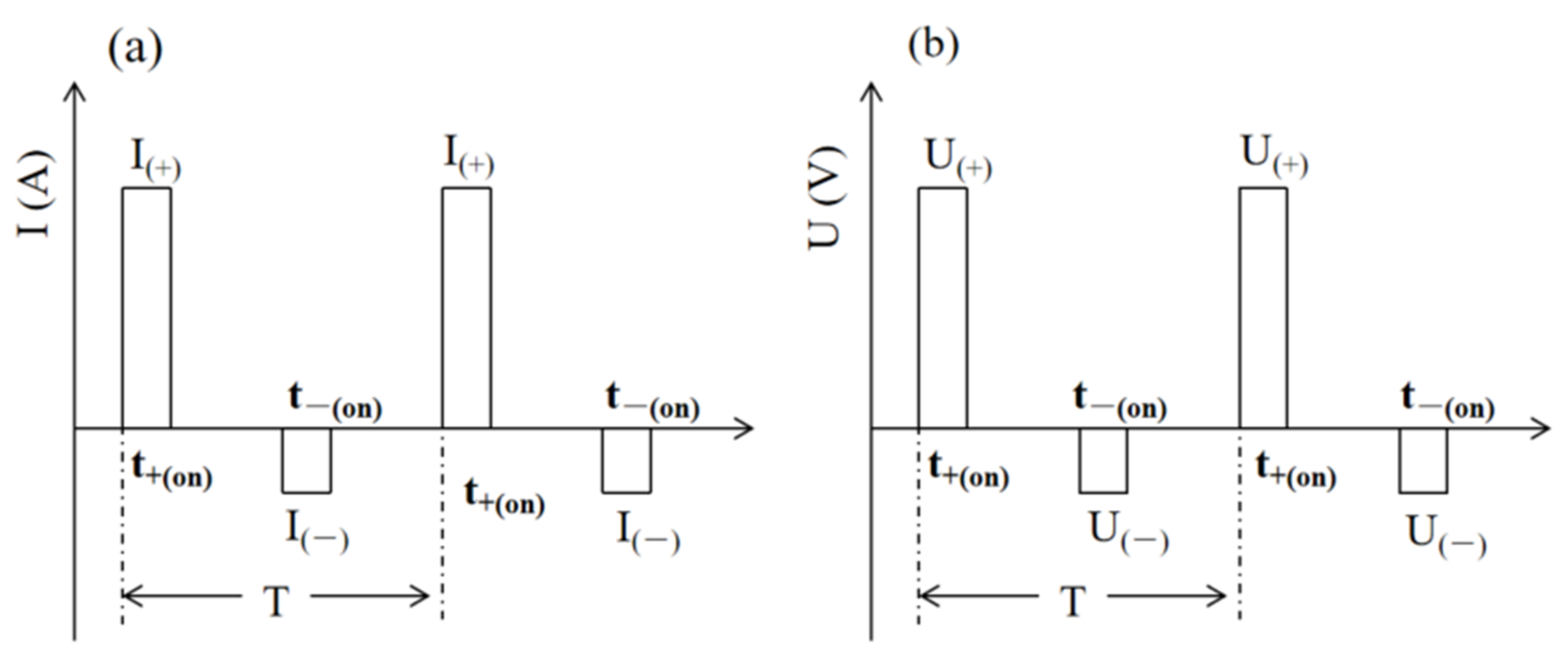
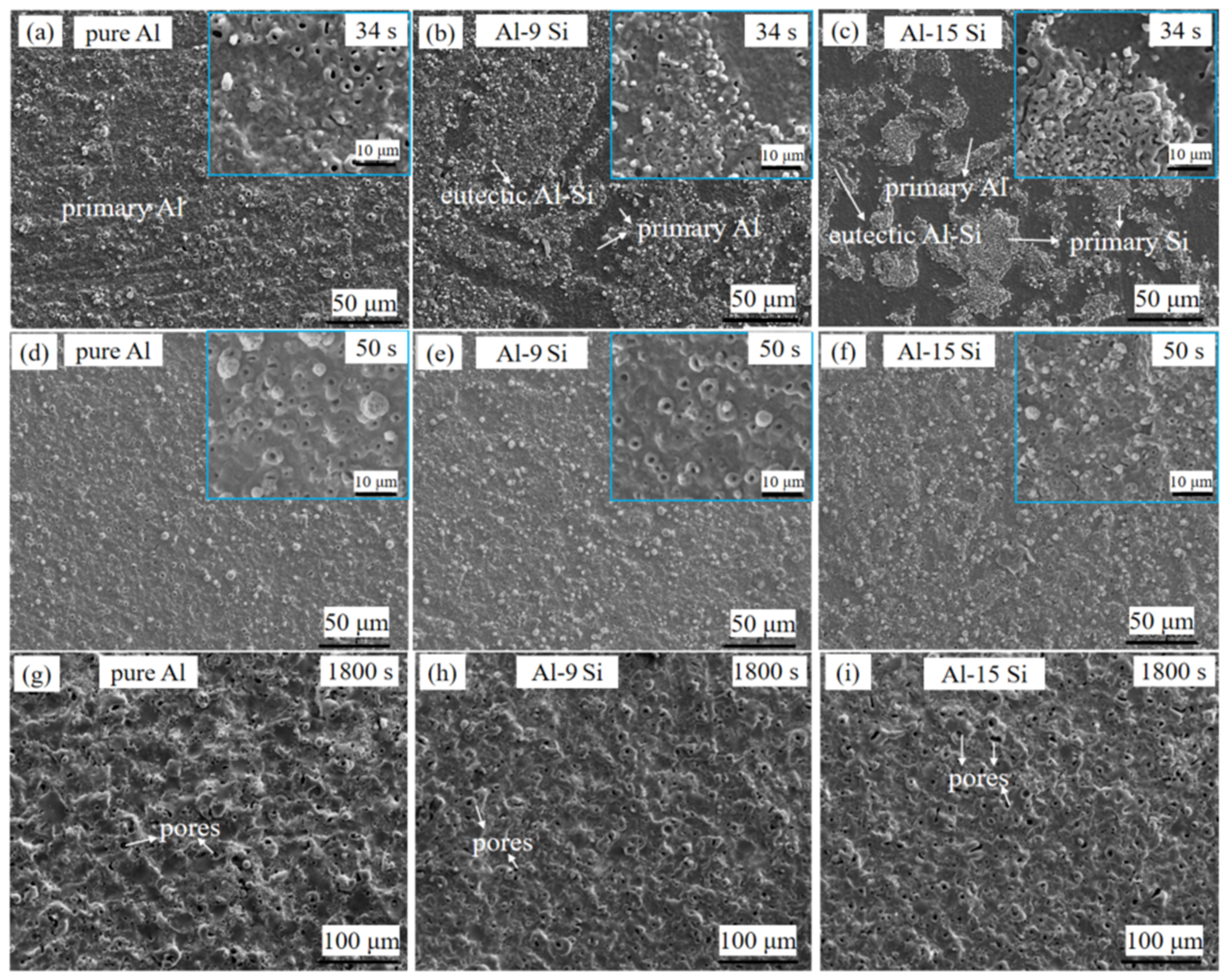
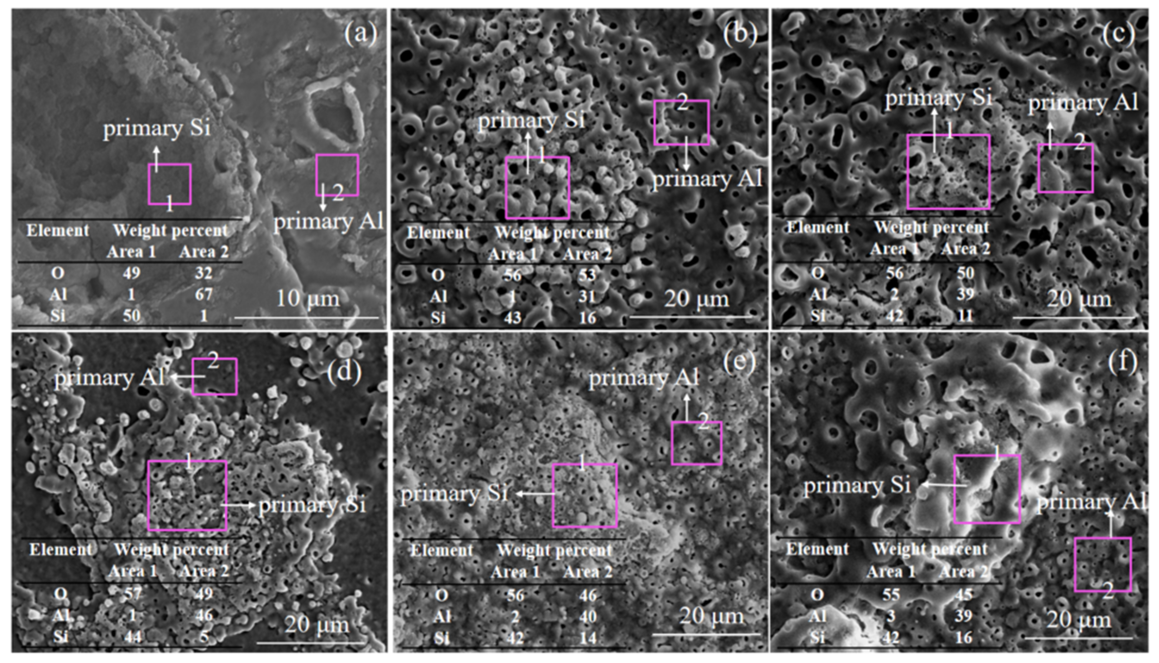
3.1. PEO of Samples Using the PBC Oxidation Mode

Figure 2 shows the relationship between the output positive voltage and the PEO processing time. The voltage curves followed a similar trend as in a previously reported case where Al-Si alloys underwent constant-current oxidation treatment [21]. At any point during the oxidation, the positive voltage decreased with increasing Si content in the substrate. However, the extent of deviation was reduced as the treatment time was prolonged. After 30 min of oxidation, the positive voltage deceased from approximately 464 to 442 V when the Si content in the matrix increased from 0 to 15 wt.%.
Figure 3 presents the surface morphologies of PEO layers on pure Al, Al-9Si, and Al-15 Si after various oxidation times in the PBC mode. The layer on the pure Al sample grew uniformly throughout the entire process (Figure 3a,d,g). However, the layers on the Al-9Si and Al-15Si samples were uneven during the initial stage of oxidation. Some coarse oxide was formed in the eutectic Si and primary Si regions, where discharge sparks preferentially occurred (Figure 3b,c). The layers on the Al-9Si and Al-15Si samples became increasingly uniform as the oxidation process continued for ~10 or 16 min, respectively (Figure 3e,f). By the end of the 30 min process, the surface morphologies of the three layers were all very flat, and the number of pores on their surfaces increased slightly with the substrate’s Si content (Figure 3g–i).
Figure 4 shows the thicknesses of the layers generated on various samples following 30 min of oxidation processing in the PBC mode. The final layer thickness decreased from 21.3 to 11.7 μm (~45%) when the Si concentration in the substrate increased from 0 to 15 wt.%. The thickness decreased almost linearly as the Si content increased from 0 to 12 wt.%, although a sharp reduction in thickness was observed when the matrix Si concentration increased from 12 to 15 wt.%.
Figure 5 shows the energy consumption of the layers on different samples following the 30 min oxidation treatment in the PBC mode. The total energy consumption decreased from 0.12 to 0.1 kWh as the Si concentration in the alloy increased from 0 to 15 wt.%, while the specific energy consumption of the layers gradually increased from 5.0 to 7.6 kWh m−2 μm−1. Additionally, a sharp change was observed in the layer specific energy consumption when the Si content in the matrix increased from 12 to 15 wt.%.
Figure 6 shows the cross-sectional morphologies of the layers on pure Al, Al-9Si, and Al-15Si after 30 min of processing in the PBC mode. The practical layer thicknesses were consistent with the tested values, as shown in Figure 4. However, some large pores with irregular shapes were distributed randomly across these layers, and a dense sub-layer existed near the matrix, which indicated good adhesion between the substrate and the ceramic coatings.

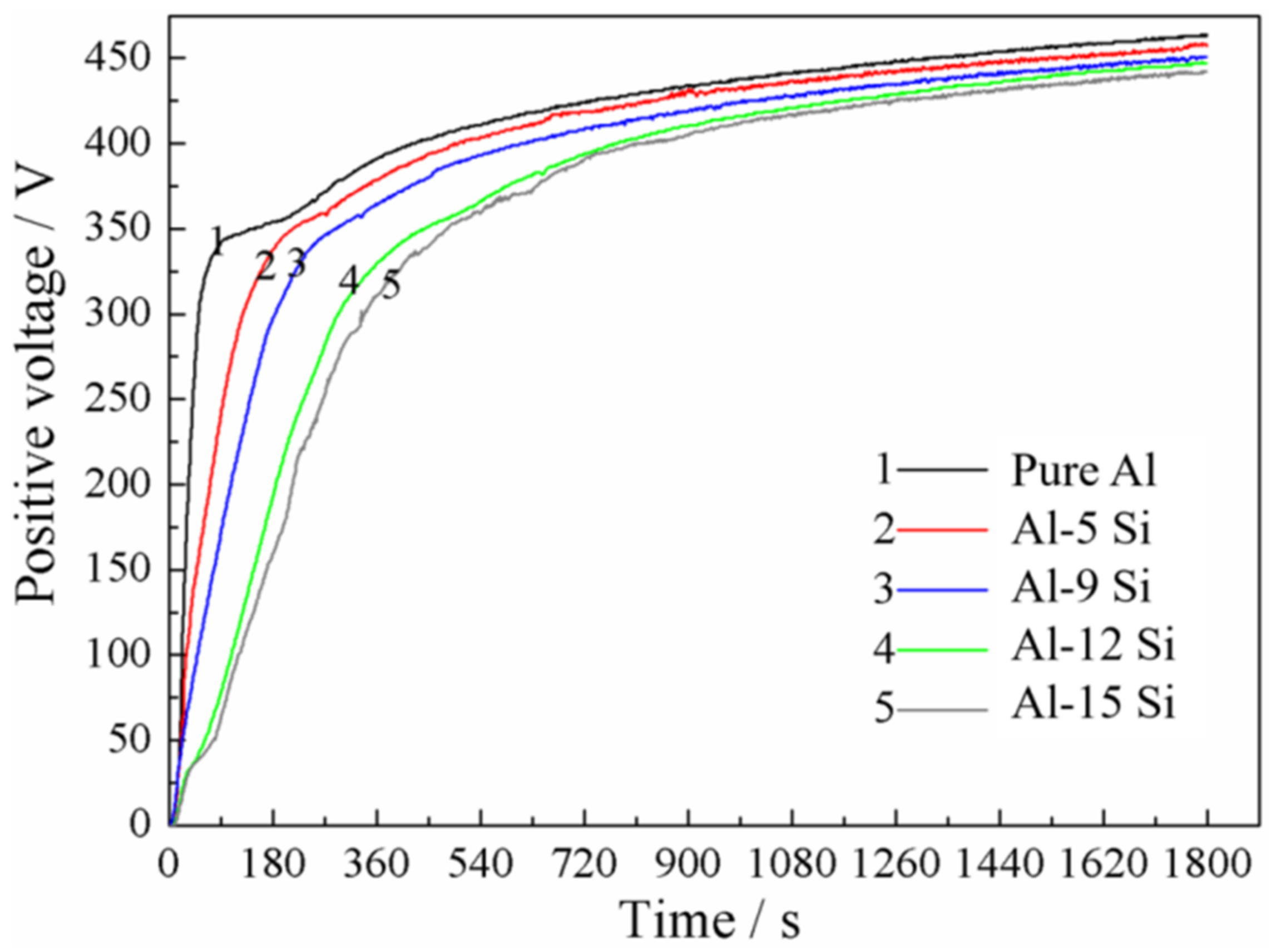
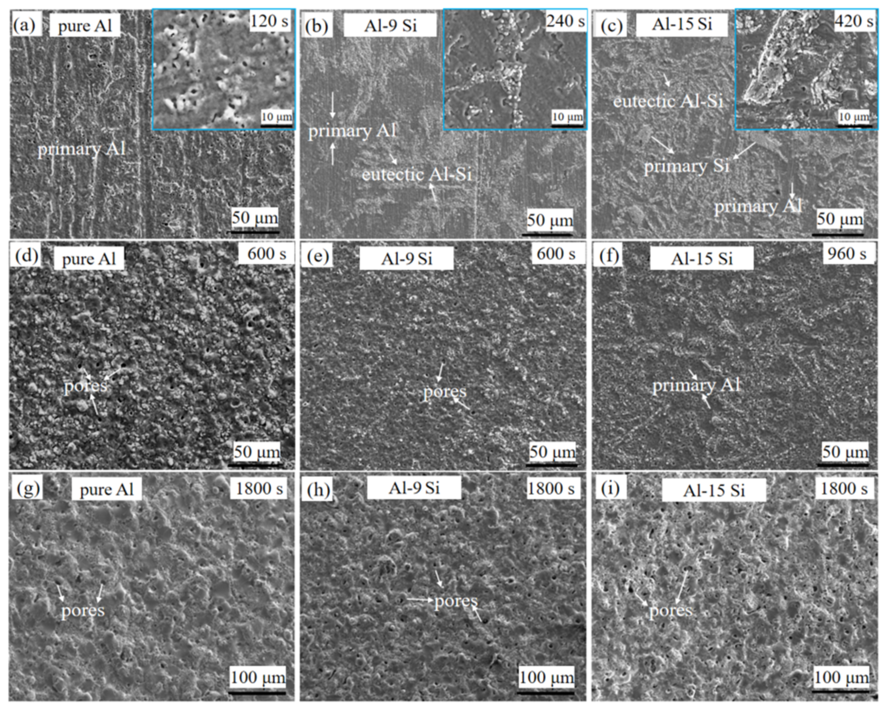
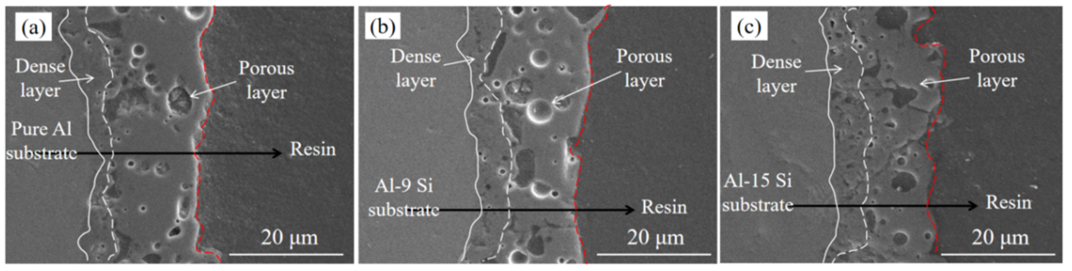
3.2. PEO of Samples Using the PBV Oxidation Mode

Figure 7 presents the positive currents of different samples over 30 min of treatment in the PBV mode. It took several dozen seconds before the output voltage reached the set value because the power supply avoided exceedingly high currents to protect itself (the membrane resistance was very small during the early stage). A similar phenomenon was observed in the PEO of ZL101 when applying a positive voltage of 530 V [18]. The current increased rapidly during the first 34 s of the oxidation process; however, the current of each Al-Si alloy sample experienced a fluctuation between 20 and 25 s, where their values decreased slightly and then began to climb again. In each case, the current reached a peak when the voltage reached 450 V, attaining maximum values of 13.7 to 26.7 A as the Si content increased from 0 to 15 wt.%. The current decreased gradually as the process continued. In general, the currents of samples containing relatively more Si grains were always higher at all points during the oxidation process.
The PEO layer on pure Al was essentially uniform throughout the entire process (Figure 8a,d,g). However, the morphologies of the layers on the Al-9Si and Al-15Si samples were uneven when the voltage reached 450 V. The coarse oxides induced by the discharge sparks were mainly generated in the eutectic Si or primary Si regions (Figure 8b,c). The morphologies of these two layers became much more uniform after 50 s of oxidation (Figure 8e,f). The pores derived from the discharge channels were distributed across most of the sample surface. By the end of the oxidation process, the layers exhibited rough surface structures, and the number of pores on the surface increased with the Si content in the substrate (Figure 8g–i).
Figure 9 illustrates the thicknesses of the layers obtained after 30 min of processing in the PBV mode. The layer thickness decreased in a generally linear fashion (from 22.4 to 19.9 μm) as the Si content in the matrix increased from 0 to 15 wt.%.
Figure 10 shows the energy consumptions of the layers on different samples following the 30 min oxidation treatment in the PBV mode. The total energy consumption of the samples increased from 0.08 to 0.18 kWh as the Si content in the matrix increased from 0 to 15 wt.%, while the specific energy consumption of the layers also increased (from 2.9 to 8.1 kWh m−2 μm−1). Moreover, the total and specific energy consumption both increased rapidly when the Si content of the samples increased from 12 to 15 wt.%.
Figure 11 shows the cross-sectional morphologies of the layers on pure Al, Al-9Si, and Al-15Si after 30 min of processing in the PBV mode. The practical thickness of each layer was consistent with the corresponding measured values (Figure 9). Although there were many pores randomly distributed across the three coatings, their inner layers adopted relatively denser structures.

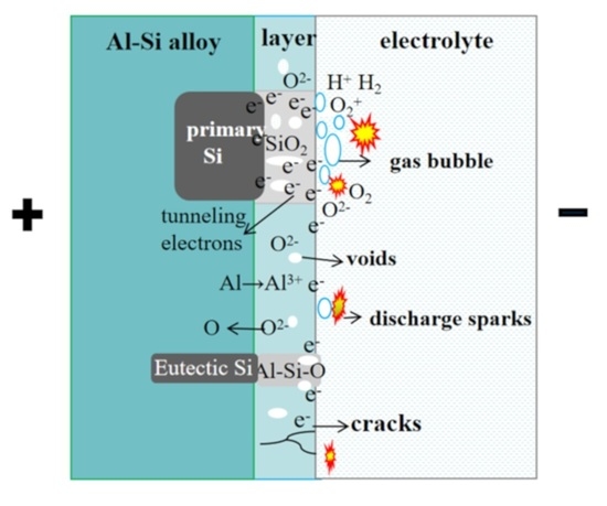
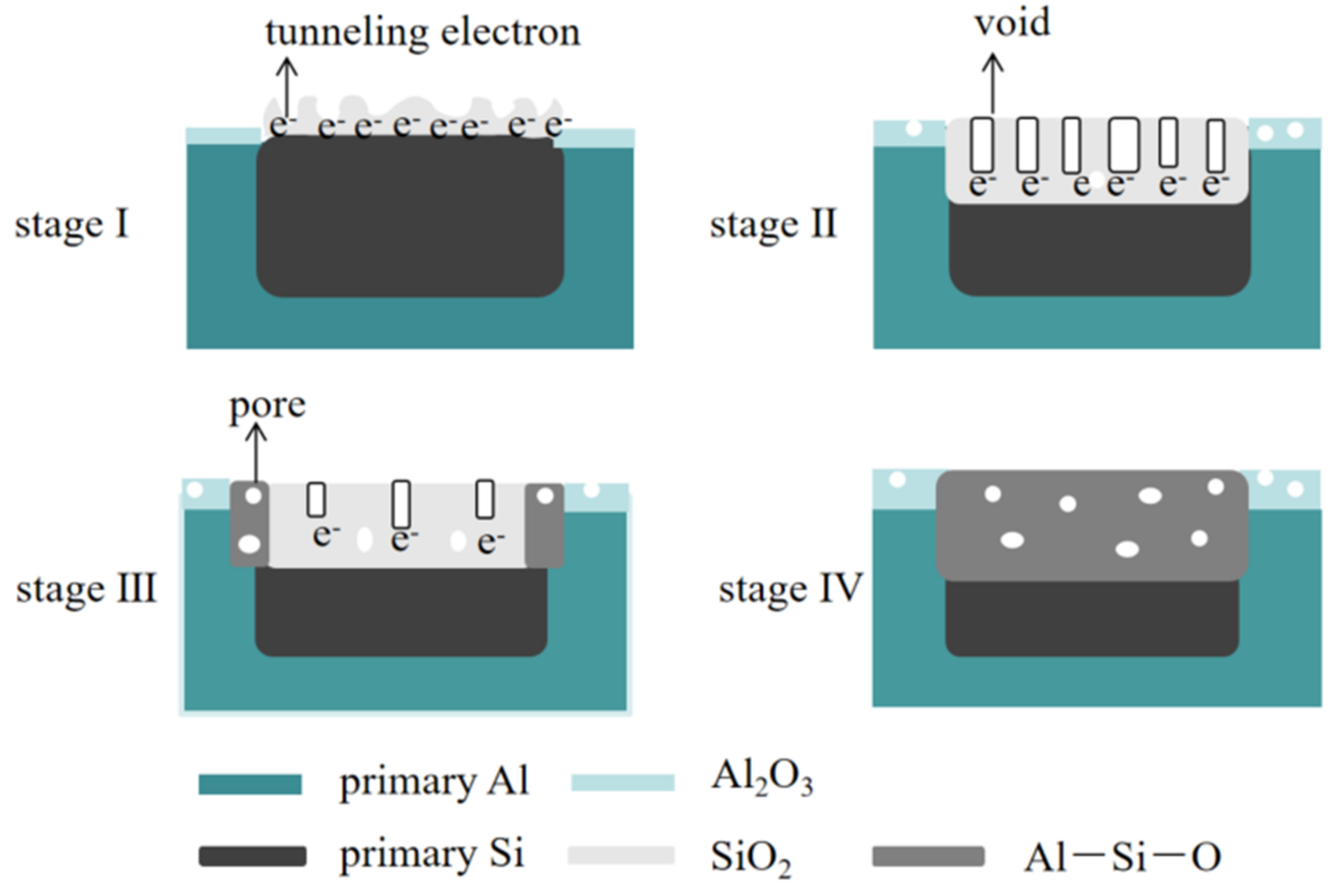
3.3. Mechanistic Analysis of the Impact of Si Grains on the PEO of Al-Si Alloys

The power supply mode plays a key role in governing the layer’s characteristics and the energy efficiency of the Al-Si alloys after a 30 min PEO treatment. This is likely related to the oxidation behavior of Si grains under different power input methods. Because it is difficult to observe the oxidation of eutectic Si owing to its small size, analyzing the oxidation process involving large primary Si might better reveal the mechanism whereby the Si phase influences the PEO processing of Al alloys. Figure 12 shows the surface morphology and composition of the PEO layer on/near the primary Si of the Al-15Si sample at the initial oxidation stage. After 270 s of oxidation in the PBC mode, a significant amount of elemental O was detected on the sample surface as SiO2 and Al2O3 films grew on the primary Si (region 1) and primary Al (region 2), respectively (Figure 12a). The volume expansion of Si to SiO2 was approximately 120%; such expansion would be hindered by the surrounding Al2O3, thus generating high stress [23]. As a result, the fragile SiO2 partially collapsed and left various defects (e.g., pits and cracks) on its surface. The discharge sparks affected the primary Al and Si regions when the oxidation process lasted for 600 s, but the SiO2 layer was still much more porous than the Al2O3 layer (Figure 12b). Additionally, numerous O, Si, and Al atoms were detected at the boundary between SiO2 and Al2O3 (region 2), which gradually converted to Al-Si-O compounds under the higher temperature condition caused by the sparks. When the oxidation treatment continued for 960 s, the SiO2 layer on the primary Si became thicker, and the voids on its surface were significantly reduced (Figure 12c). The interface between SiO2 and Al2O3 disappeared, and these phases mixed at their boundary, where Al, Si, and O elements were abundant (region 2). However, at the central part of the SiO2 layer, the Al elemental content was still relatively low (region 1). Still, an SiO2 layer containing numerous small voids was generated on the primary Si (region 1) after 34 s of oxidation in the PBV mode (Figure 12d). In contrast, only a few voids appeared on the Al2O3 film (region 2) because the discharge sparks mainly impacted the SiO2 at this point. A few seconds later, the discharge sparks covered the entire sample surface (Figure 12e). The area and number of voids on the SiO2 layer decreased substantially (region 1), and the SiO2 and Al2O3 began to mix together (region 2). When the oxidation treatment continued for 300 s, the SiO2 layer became much thicker and denser (Figure 12f, region 1). The boundary between the primary Al and Si regions disappeared as more SiO2 and Al2O3 mixed together and converted to Al-Si-O compounds (region 2). The oxidation of primary Si was significantly accelerated in the PBV mode because strong discharges occurred rapidly on its surface, which resulted in a much weaker effect of the Si content on the layer growth rate for the evaluated samples over 30 min of processing.
According to the experimental results described above, a growth model for the oxide layer on the Si grains was established and is schematically illustrated in Figure 13. In stage I, an anodic Al2O3 with few defects grew rapidly on the surface of the Al phase, while a thin anodic SiO2 film with numerous defects (e.g., voids and cracks) grew on the surface of the Si phase. The width of the tunnel barrier for Al2O3 was approximately 127 Å, while that for SiO2 was 42 Å [33]. Electrons tunneled through the porous SiO2 thin film, and gas bubble generation was promoted on the surface of oxidized Si grains [33,34]; a significant amount of electrical energy would be exhausted by the side reactions in this case (i.e., water electrolysis). However, electron tunneling through the relatively denser and thicker Al2O3 was limited because appreciable electron tunneling only becomes favorable when the width of the barrier is less than 100 Å [33]. In stage Ⅱ, the discharge sparks began to occur as the voltage exceeded a threshold value. The theoretical resistance of SiO2 is approximately 1010 Ω·cm−1, which is four orders of magnitude lower than that of Al2O3 [35,36]. Therefore, dielectric breakdown preferentially occurred on the SiO2 film, rather than on the Al2O3 film. The electrons tunneling through the thin regions of the SiO2 film still promoted the generation of gas bubbles. Some bubbles could become trapped in the oxides during the chilling process. Thus, many voids existed on the surface of the SiO2 layer. When the resistance of SiO2 increased and approached that of Al2O3, the oxidation process entered stage III, wherein the discharge sparks occurred on the anodic Al2O3 layer as well. The electron tunneling phenomenon was reduced significantly as the SiO2 layer grew much thicker. The number of voids in the SiO2 layer also decreased, and the SiO2 and Al2O3 gradually converted to Al-Si-O compounds. As a result, the SiO2 had a much weaker influence on the layer growth thereafter. Once the SiO2 had mostly converted to mullite, the process reached stage IV, wherein the effect of SiO2 on the PEO process was weak. The oxide layer exhibited a much more uniform morphology containing few voids on its surface.
The oxidations of primary Si and eutectic Si to SiO2 were essentially the same; however, it was difficult for the large SiO2 to mix with the Al2O3 to produce mullite. In general, the negative effect of primary Si on the PEO of Al-Si alloys would last for a much longer time than in the case of eutectic Si. Moreover, the size and number of Si grains were directly correlated with the Si concentration in the substrate. Therefore, the layer thickness was reduced, and the specific energy consumption increased appreciably as the matrix Si content increased during a 30 min process in either the PBC or PBV mode. Both of these parameters changed more significantly when the Si content increased from 12 to 15 wt.%, because there were numerous bulk Si grains in the Al-15Si alloy. In addition, the oxidation of Si grains was accelerated in the PBV mode relative to the PBC mode. The layer growth entered stage IV quickly, which meant that the effect of SiO2 on the layer growth weakened within a few minutes. Thus, the layer thicknesses in different samples following 30 min of PBV oxidation treatment were very similar. However, the positive current clearly increased as the Si content increased during the first 5 min of processing (i.e., when the energy consumption contributed a major portion of the overall energy). A greater amount of energy was exhausted by the side reactions or resistance heat for the sample with the highest Si mass. Thus, the specific energy consumption of the final layer increased significantly with the matrix Si content in the PBV mode.

4. Conclusions

In this study, pure Al and Al alloys containing 5, 9, 12, and 15 wt.% Si were treated via PEO for 30 min in pulsed bipolar current and pulsed bipolar voltage power modes. The main conclusions drawn from the results are as follows:
(1)
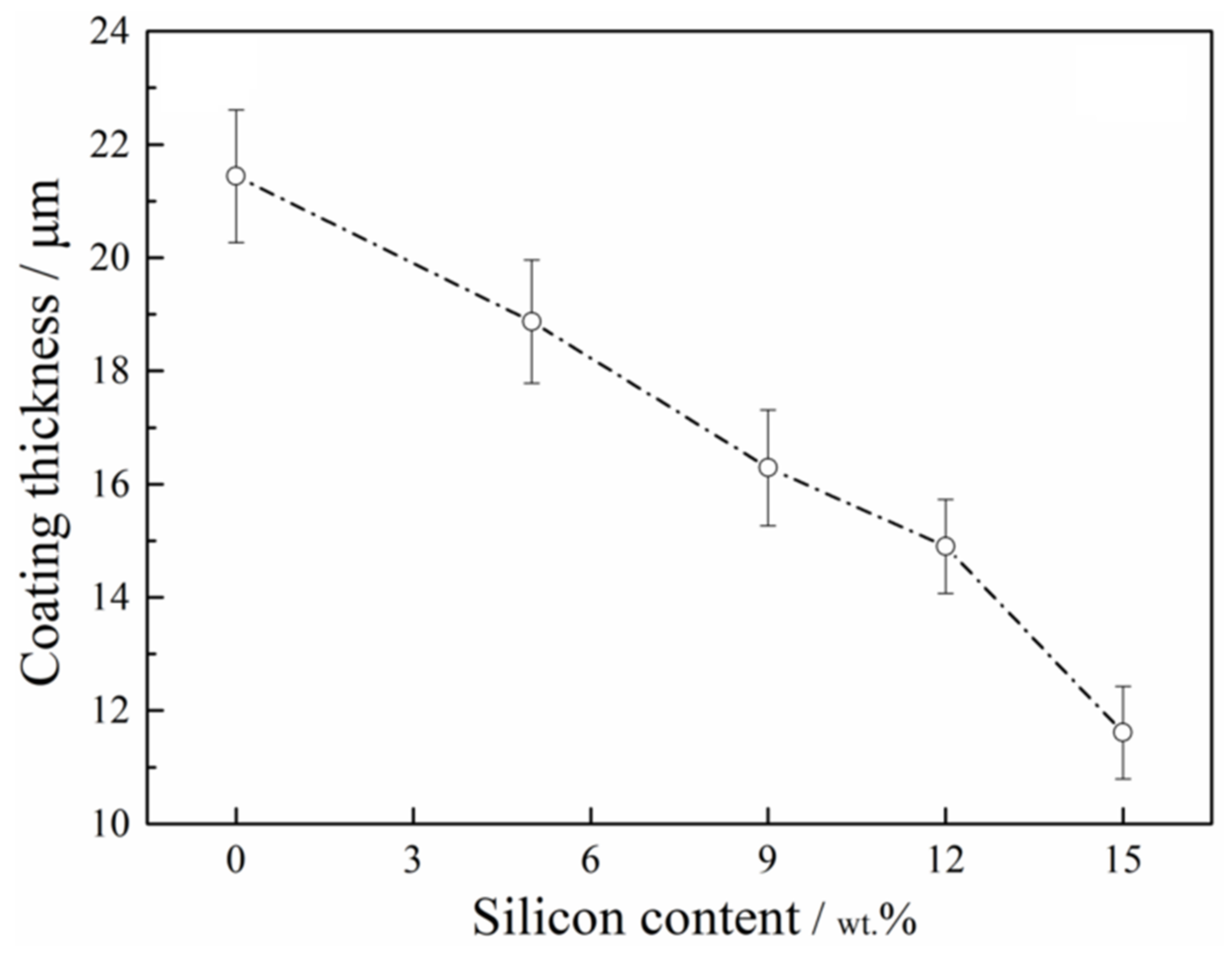
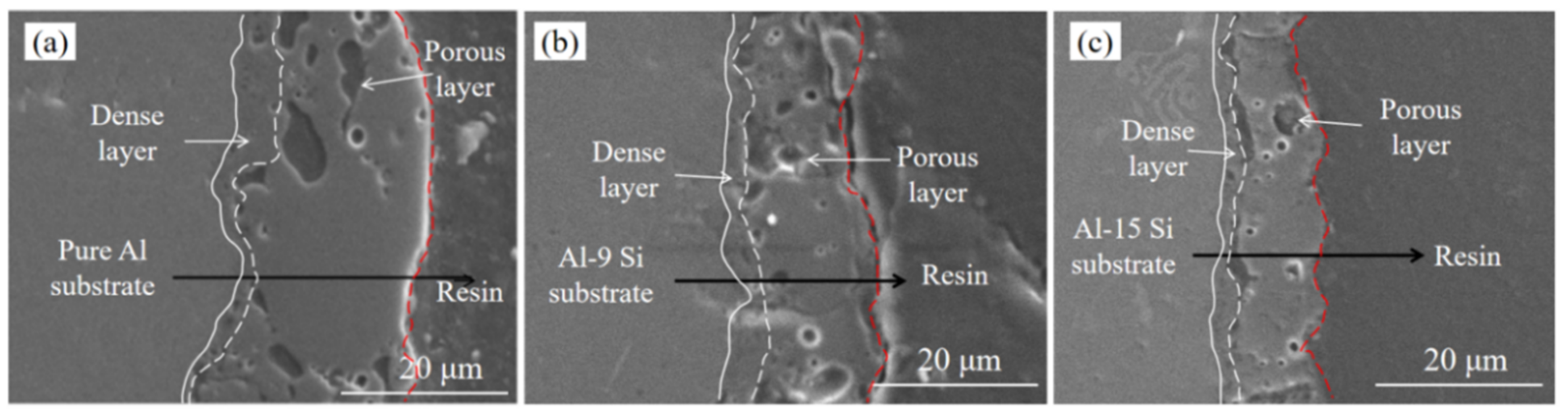
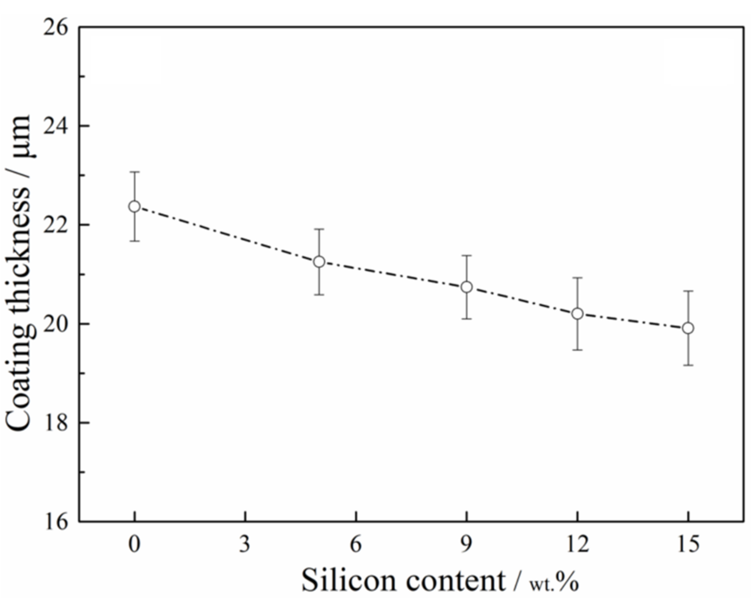
The eutectic Si and primary Si grains had slow oxidation rates when using the pulsed bipolar voltage mode. It took a long time for the SiO2 growing on the large Si grains to mix with the surrounding Al2O3 to generate Al-Si-O compounds. The negative effect of porous SiO2 on the PEO process continued for a longer time in the Al alloy containing larger Si grains; therefore, the final layer thicknesses on different Al alloys decreased significantly with increasing Si content in the matrix;
(2)
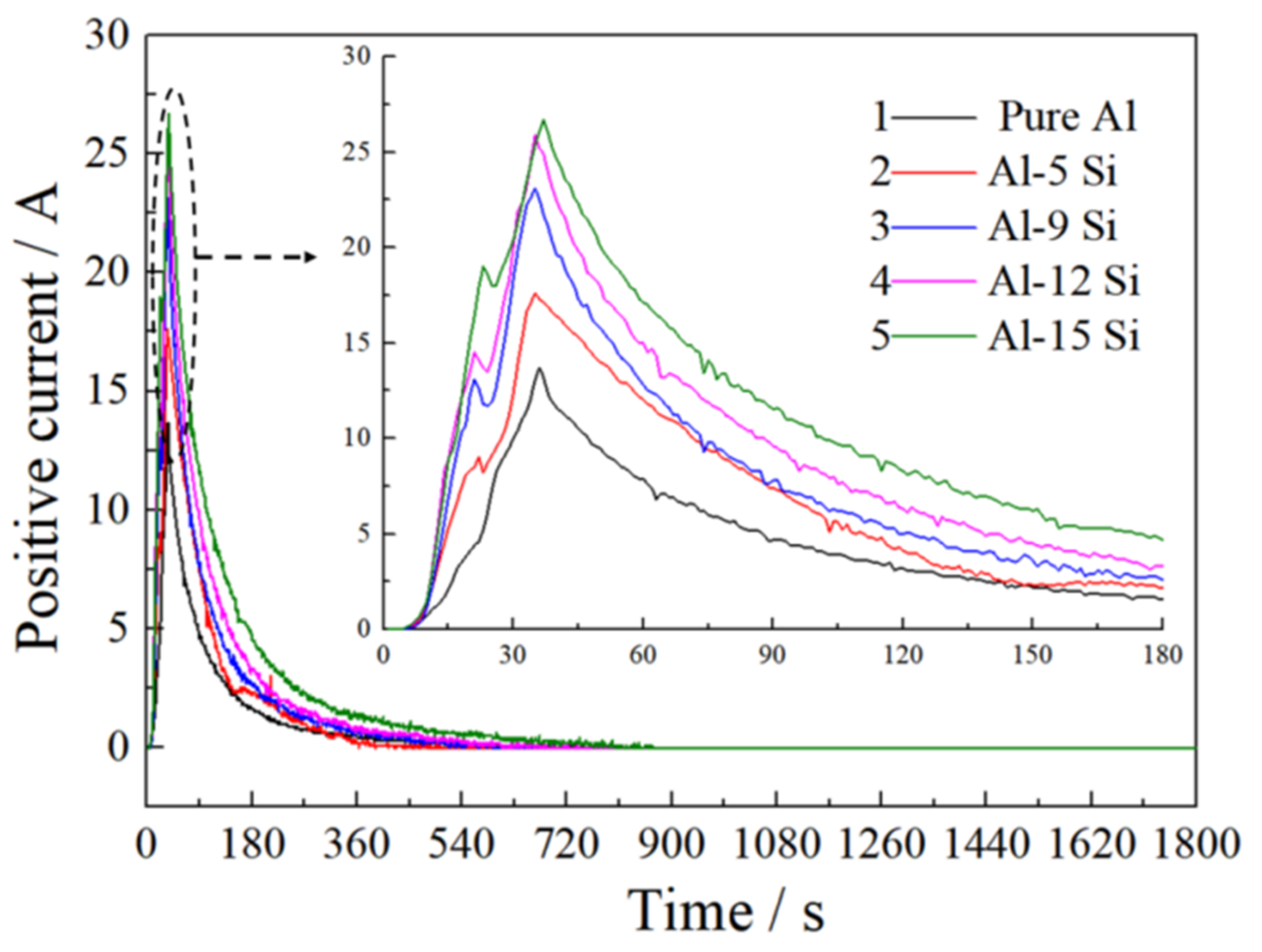
The eutectic Si and primary Si grains were rapidly oxidized and converted to Al-Si-O compounds when using the pulsed bipolar current mode. The effect of Si or SiO2 on the layer growth process weakened after a short period of oxidation, such that the layer thicknesses on different Al alloys were very similar by the end of the pulsed bipolar voltage oxidation process;
(3)
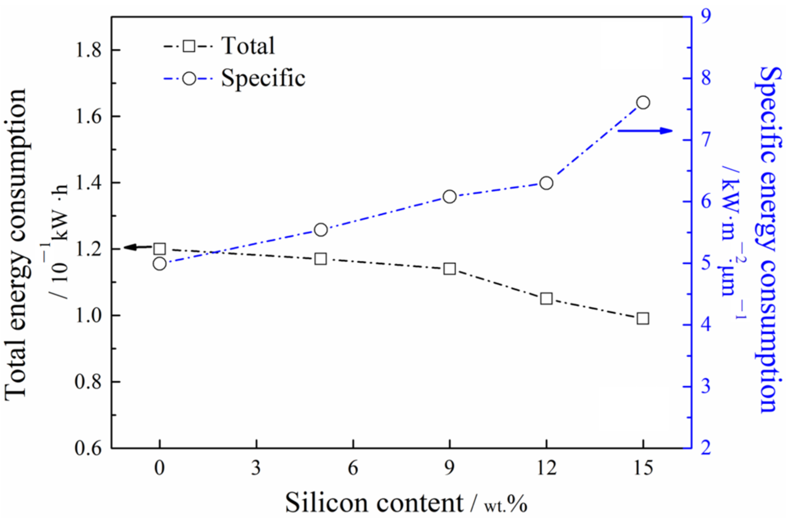
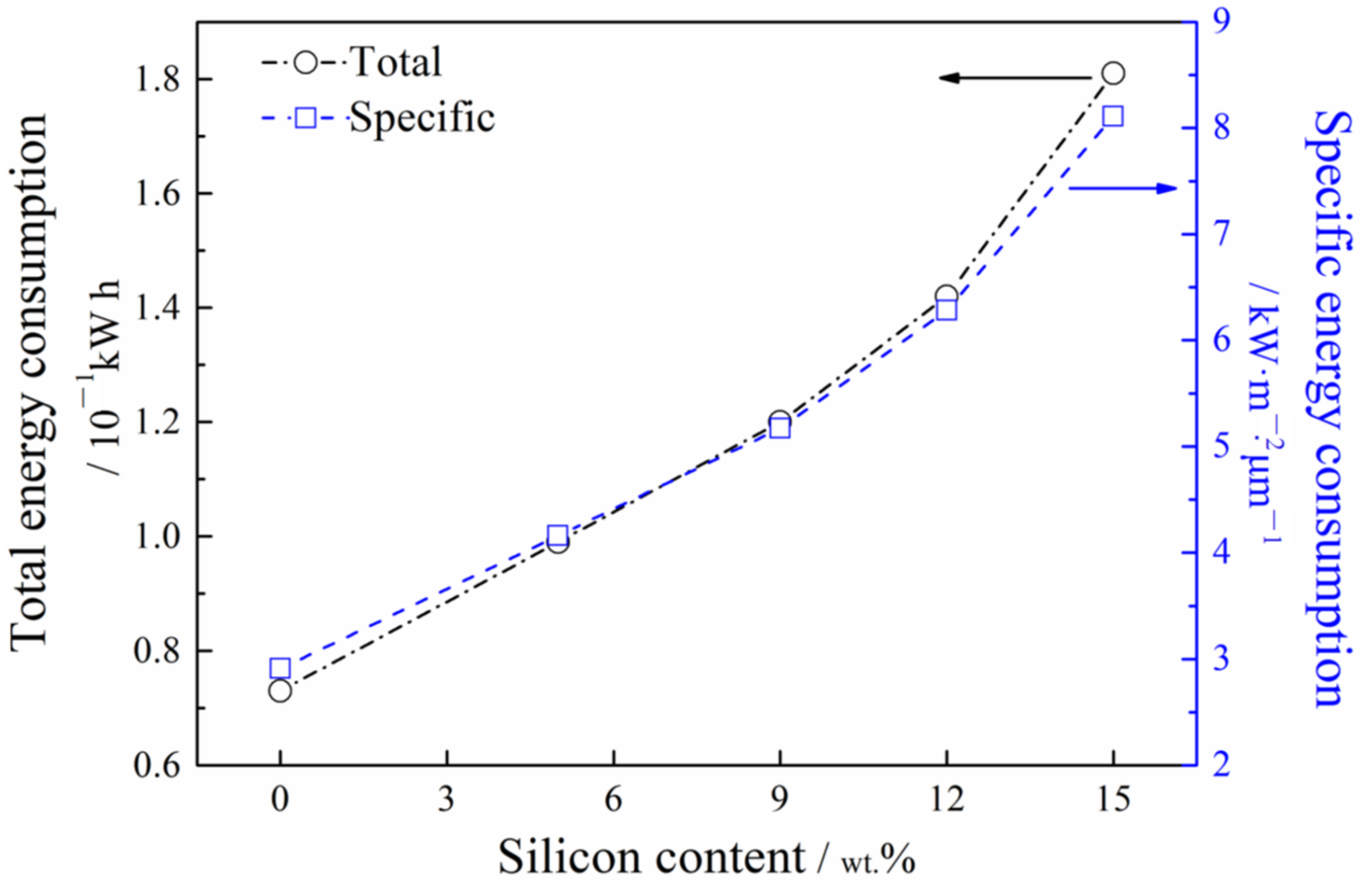
The specific energy consumption of the layers decreased as the Si content increased, regardless of whether the pulsed bipolar current or pulsed bipolar voltage mode was applied.

Author Contributions

Conceptualization, W.L.; investigation, K.L., W.Z. and A.Y.; writing—original draft preparation, K.L. and Z.L. (Zhongmiao Liao); writing—review and editing, G.Z., K.C. and Z.L. (Zhenyuan Luo). All authors have read and agreed to the published version of the manuscript.

Funding

This research was funded by the Guangdong Basic and Applied Basic Research Foundation (Grant No. 2019A1515110466), the Guangzhou Science and Technology Department (Project No. 202002030058), the Research Start-up funds of DGUT (Project No. 211135059), the Development Project (Key) of Dongguan Social Science and Technology (Grant No. 2020507140151), the Innovative Team Project of Guangdong University (Project No. 2021KCXTD022), the Applied Basic Research of High Performance Metal Additive Manufacturing Materials and Process (Project No. 2140064), the Novel Light Alloy and its Process Technology Key Laboratory of Dongguan City, and the Guangdong Research Center of High Performance Light Alloys Forming Technology.

Institutional Review Board Statement

Not applicable.

Informed Consent Statement

Not applicable.

Data Availability Statement

Not applicable.

Conflicts of Interest

The authors declare no conflict of interest.

References

  1. Chen, J.Q.; Wen, F.; Liu, C.; Li, W.R.; Zhou, Q.Y.; Zhu, W.C.; Zhang, Y.H.; Guan, R.G. The microstructure and property of Al-Si alloy improved by the Sc-microalloying and Y2O3 nano-particles. Sci. Technol. Adv. Mater. 2021, 22, 205–217. [Google Scholar] [CrossRef]
  2. Huang, J.M.; Zhao, H.D.; Chen, Z.M. Microstructure and properties of A356 alloy wheels fabricated by low-pressure die casting with local squeeze. J. Mater. Eng. Perform. 2019, 28, 2137–2146. [Google Scholar] [CrossRef]
  3. Martin, J.H.; Yahat, B.D.; Hundley, J.M.; Mayer, J.A.; Schaedler, T.A.; Pollock, T.M. 3D printing of high-strength aluminium alloys. Nature 2017, 549, 365–369. [Google Scholar] [CrossRef]
  4. Cabrini, M.; Lorenzi, S.; Pastore, T.; Testa, C.; Manfredi, D.; Lorusso, M.; Calignano, F.; Pavese, M.; Andreatta, F. Corrosion behavior of AlSi10Mg alloy produced by laser powder bed fusion under chloride exposures. Corros. Sci. 2019, 152, 101–108. [Google Scholar] [CrossRef]
  5. Rogov, A.B.; Lyu, H.; Matthews, A.; Yerokhin, A. AC plasma electrolytic oxidation of additively manufactured and cast AlSi12 alloys. Surf. Coat. Technol. 2020, 399, 126116. [Google Scholar] [CrossRef]
  6. Pezzato, L.; Dabalà, M.; Gross, S.; Brunelli, K. Effect of microstructure and porosity of AlSi10Mg alloy produced by selective laser melting on the corrosion properties of plasma electrolytic oxidation coatings. Surf. Coat. Technol. 2020, 404, 126477. [Google Scholar] [CrossRef]
  7. Zhu, B.W.; Zanella, C. Hardness and corrosion behaviour of anodised Al-Si produced by rheocasting. Mater. Des. 2019, 173, 107764. [Google Scholar] [CrossRef]
  8. Lien, H.H.; Mazumder, J.; Wang, J.; Misra, A. Microstructure evolution and high density of nanotwinned ultrafine Si in hypereutectic Al-Si alloy by laser surface remelting. Mater. Charact. 2020, 161, 110147. [Google Scholar] [CrossRef]
  9. Mora-Sanchez, H.; Olmo, R.; Rams, J.; Torres, B.; Mohedano, M.; Matykina, E.; Arrabal, R. Hard Anodizing and Plasma Electrolytic Oxidation of an Additively Manufactured Al-Si alloy. Surf. Coat. Technol. 2021, 420, 127339. [Google Scholar] [CrossRef]
  10. Wang, P.; Wang, P.; Yuwen, Q.Q.; Li, J.P. The differences in the formation mechanism of PEO and CPED composited ceramic coatings on Al-12Si alloy. J. Alloys Compd. 2019, 788, 61–66. [Google Scholar] [CrossRef]
  11. Walsh, F.C.; Low, C.T.J.; Wood, R.J.K.; Stevens, K.T.; Archer, J.; Poeton, A.R.; Ryder, A. Plasma electrolytic oxidation (PEO) for production of anodised coatings on lightweight metal (Al, Mg, Ti) alloys. Trans. Inst. Met. Finish. 2009, 87, 122–135. [Google Scholar] [CrossRef]
  12. Shi, X.T.; Wang, Y.; Li, H.Y.; Zhang, S.F.; Zhao, R.F.; Li, G.Q.; Zhang, R.F.; Sheng, Y.; Cao, S.Y.; Zhao, Y.J.; et al. Corrosion resistance and biocompatibility of calcium-containing coatings developed in near-neutral solutions containing phytic acid and phosphoric acid on AZ31B alloy. J. Alloys Compd. 2020, 823, 153721. [Google Scholar] [CrossRef]
  13. Javidi, M.; Fadaee, H. Plasma electrolytic oxidation of 2024-T3 aluminum alloy and investigation on microstructure and wear behavior. Appl. Surf. Sci. 2013, 286, 212–219. [Google Scholar] [CrossRef]
  14. Tran, Q.P.; Chin, T.S.; Kuo, Y.C.; Jin, C.X.; Trung, T.; Tuan, C.V.; Dang, D.Q. Diamond powder incorporated oxide layers formed on 6061 Al alloy by plasma electrolytic oxidation. J. Alloys Compd. 2018, 751, 289–298. [Google Scholar] [CrossRef]
  15. Haghighat-Shishavan, B.; Azari-Khosrowshahi, R.; Haghighat-Shishavan, S.; Nazarian-Samani, M.; Parvini-Ahmadi, N. Improving wear and corrosion properties of alumina coating on AA7075 aluminum by plasma electrolytic oxidation: Effects of graphite absorption. Appl. Surf. Sci. 2019, 481, 108–119. [Google Scholar] [CrossRef]
  16. Movahedi, N.; Habibolahzadeh, A. Effect of plasma electrolytic oxidation treatment on corrosion behavior of closed-cell Al-A356 alloy foam. Mater. Lett. 2016, 164, 558–561. [Google Scholar] [CrossRef]
  17. Yu, H.J.; Dong, Q.; Chen, Y.; Chen, C.Z. Influence of silicon on growth mechanism of micro-arc oxidation coating on cast Al-Si alloy. R. Soc. Open Sci. 2018, 5, 172428. [Google Scholar] [CrossRef] [Green Version]
  18. Xue, W.B.; Shi, X.L.; Hua, M.; Li, Y.L. Preparation of anti-corrosion films by micro arc oxidation on an Al-Si alloy. Appl. Surf. Sci. 2007, 253, 6118–6124. [Google Scholar] [CrossRef]
  19. Zhu, M.H.; Cai, Z.B.; Lin, X.Z.; Ren, P.D.; Tan, J.; Zhou, Z.R. Fretting wear behaviour of ceramic coating prepared by micro-arc oxidation on Al-Si alloy. Wear 2007, 263, 472–480. [Google Scholar] [CrossRef]
  20. Krishna, L.R.; Purnima, A.S.; Wasekar, N.P.; Sundararajan, G. Kinetics and properties of micro arc oxidation coatings deposited on commercial Al alloys. Metall. Mater. Trans. A 2007, 38, 370–378. [Google Scholar] [CrossRef]
  21. Wang, L.; Nie, X. Silicon effects on formation of EPO oxide coatings on aluminum alloys. Thin Solid Films 2006, 494, 211–218. [Google Scholar] [CrossRef]
  22. Wang, P.; Li, J.P.; Guo, Y.C.; Yang, Z.; Wang, J.L. Ceramic coating formation on high Si containing Al alloy by PEO process. Surf. Eng. 2016, 32, 428–434. [Google Scholar] [CrossRef]
  23. Xu, F.T.; Cai, Z.B.; Li, G. The mechanism of PEO process on Al-Si alloys with the bulk primary silicon. Appl. Surf. Sci. 2009, 255, 951–953. [Google Scholar] [CrossRef]
  24. Gulec, A.E.; Gencer, Y.; Tarakci, M. The characterization of oxide based ceramic coating synthesized on Al-Si binary alloys by microarc oxidation. Surf. Coat. Technol. 2015, 269, 100–107. [Google Scholar] [CrossRef]
  25. Mohedano, M.; Matykina, E.; Arrabal, R.; Mingo, B.; Zheludkevich, M.L. PEO of rheocast A356 Al alloy: Energy efficiency and corrosion properties. Surf. Interface Anal. 2016, 48, 953–959. [Google Scholar] [CrossRef]
  26. Li, K.; Li, W.F.; Zhang, G.G.; Zhu, W.; Zheng, F.H.; Zhang, D.Q.; Wang, M. Effects of Si phase refinement on the plasma electrolytic oxidation of eutectic Al-Si alloy. J. Alloys Compd. 2019, 790, 650–656. [Google Scholar] [CrossRef]
  27. Li, K.; Li, W.F.; Yi, A.H.; Zhu, W.; Liao, Z.M.; Chen, K.; Li, W.M. Tuning the Surface Characteristic of Al-Si Alloys and Its Impacts on the Formation of Micro Arc Oxidation Layers. Coatings 2021, 11, 453. [Google Scholar] [CrossRef]
  28. Hwang, I.J.; Hwang, D.Y.; Kim, Y.M.; Yoo, B.; Shin, D.H. Formation of uniform passive oxide layers on high Si content Al alloy by plasma electrolytic oxidation. J. Alloys Compd. 2010, 504, S527–S530. [Google Scholar] [CrossRef]
  29. Fernández-López, P.; Alves, S.A.; López-Ortega, A.; Jośe-Lombera, J.T.S.; Bayon, R. High performance tribological coatings on a secondary cast Al–Si alloy generated by Plasma Electrolytic Oxidation. Ceram. Int. 2021, 47, 31238–31250. [Google Scholar] [CrossRef]
  30. Mohedano, M.; Matykina, E.; Arrabal, R.; Mingo, B.; Pardo, A. PEO of pre-anodized Al–Si alloys: Corrosion properties and influence of sealings. Appl. Surf. Sci. 2015, 346, 57–67. [Google Scholar] [CrossRef]
  31. Fu, J.G.; Li, M.; Liu, G.S.; Ma, S.L.; Zhu, X.H.; Ma, C.S.; Cheng, D.; Yan, Z.J. Robust ceramic based self-lubricating coating on Al-Si alloys prepared via PEO and spin-coating methods. Wear 2020, 458–459, 203405. [Google Scholar] [CrossRef]
  32. Hussein, R.O.; Nie, X.; Northwood, D.O.; Yerokhin, A.; Matthews, A. Spectroscopic study of electrolytic plasma and discharging behaviour during the plasma electrolytic oxidation (PEO) process. J. Phys. D Appl. Phys. 2010, 43, 105203. [Google Scholar] [CrossRef]
  33. Vijh, A.K. Sparking voltages and side reactions during anodization of valve metals in terms of electron tunneling. Corros. Sci. 1971, 11, 411–417. [Google Scholar] [CrossRef]
  34. Okorn-Schmidt, H.F. Characterization of silicon surface preparation processes for advanced gate dielectrics. IBM J. Res. Dev. 1999, 43, 351–365. [Google Scholar] [CrossRef]
  35. Adams, M. Ceramic Material Characteristics [EB/OL]. 2013. Available online: http://accuratus.com/materials.html (accessed on 14 May 2021).
  36. Clyne, T.W.; Troughton, S.C. A review of recent work on discharge characteristics during plasma electrolytic oxidation of various metals. Int. Mater. Rev. 2019, 64, 127–162. [Google Scholar] [CrossRef] [Green Version]
Figure 1. Diagrams illustrating the output signals in the pulsed bipolar (a) current and (b) voltage power supply modes.
Crystals 12 00123 g001
Figure 2. Variation in the positive voltage with prolonged processing time in the PBC mode.
Crystals 12 00123 g002
Figure 3. Surface morphologies of the PEO layers on (a,d,g) pure Al, (b,e,h) Al-9Si, and (c,f,i) Al-15Si after different processing times in the PBC mode.
Crystals 12 00123 g003
Figure 4. Thickness of the PEO layer on different samples after a 30 min oxidation process in the PBC mode.
Crystals 12 00123 g004
Figure 5. Thickness of the PEO layers on different samples after a 30 min oxidation process in the PBC mode.
Crystals 12 00123 g005
Figure 6. Cross-sectional images of (a) pure Al, (b) Al-9Si, and (c) Al-15Si after processing for 30 min in the PBC mode.
Crystals 12 00123 g006
Figure 7. Variations in the positive current as a function of the processing time in the PBV mode.
Crystals 12 00123 g007
Figure 8. Surface morphologies of (a,d,g) pure Al, (b,e,h) Al-9Si, and (c,f,i) Al-15Si after different PBV processing times.
Crystals 12 00123 g008
Figure 9. Thicknesses of the layers on different samples in the PBV mode.
Crystals 12 00123 g009
Figure 10. Total and specific energy consumption of the layers on samples after 30 min of oxidation processing in the PBV mode.
Crystals 12 00123 g010
Figure 11. Cross-sectional images of (a) pure Al, (b) Al-9Si, and (c) Al-15Si after processing for 30 min in the PBV mode.
Crystals 12 00123 g011
Figure 12. Morphology and EDS analysis of the layers on Al−15Si after (a) 270, (b) 600, or (c) 960 s of processing in the PBC mode, or (d) 34, (e) 50, or (f) 300 s of processing in the PBV mode.
Crystals 12 00123 g012
Figure 13. Schematic diagram of the oxidation process involving an Al-Si alloy undergoing PEO treatment.
Crystals 12 00123 g013
Publisher’s Note: MDPI stays neutral with regard to jurisdictional claims in published maps and institutional affiliations.

