Article

Low Forward Voltage III-Nitride Red Micro-Light-Emitting Diodes on a Strain Relaxed Template with an InGaN Decomposition Layer

1
Materials Department, University of California, Santa Barbara, CA 93106, USA
2
Department of Electrical and Computer Engineering, University of California, Santa Barbara, CA 93106, USA
3
Department of Chemical Engineering, University of California, Santa Barbara, CA 93106, USA
*
Author to whom correspondence should be addressed.
Crystals 2022, 12(5), 721; https://doi.org/10.3390/cryst12050721
Submission received: 21 April 2022 / Revised: 17 May 2022 / Accepted: 17 May 2022 / Published: 19 May 2022
(This article belongs to the Special Issue GaN-Based Materials and Devices)

Abstract

:
In this study, III-nitride red micro-light-emitting diodes (µLEDs) with ultralow forward voltage are demonstrated on a strain relaxed template. The forward voltage ranges between 2.00 V and 2.05 V at 20 A/cm2 for device dimensions from 5 × 5 to 100 × 100 µm2. The µLEDs emit at 692 nm at 5 A/cm2 and 637 nm at 100 A/cm2, corresponding to a blueshift of 55 nm due to the screening of the internal electric field in the quantum wells. The maximum external quantum efficiency and wall-plug efficiency of µLEDs are 0.31% and 0.21%, respectively. This suggests that efficient III-nitride red µLEDs can be realized with further material optimizations.

1. Introduction

Due to the rapid advancements in micro-light-emitting diodes (µLEDs) for next-generation display applications, significant research attention has been devoted to develop full-color µLED displays [1,2,3]. Moreover, monolithic III-nitride-based µLEDs are especially interesting for near-eye display applications, since this approach offers advantages in terms of fabrication and mass transfer [4,5,6].
Among the three required colors, III-nitride red µLEDs remain a critical challenge due to the increased strain in the active region attributed to the 10% lattice mismatch between InN and GaN [7]. Therefore, several novel methods have been demonstrated to reveal the possibility of III-nitride red LEDs by employing strain engineering in the active region, such as semi-relaxed InGaN substrates and porous GaN pseudo-substrates [8,9,10,11,12,13]. However, most of the proposed techniques require patterning and regrowth, which can be problematic for scalability and manufacturing perspectives. Recently, novel planar InGaN strain relaxed templates (SRTs) with more than 85% biaxially relaxation have been realized, and red LEDs using this type of template have been demonstrated [14,15]. In these reports, the SRTs consist of a thin layer with a high indium composition of InGaN decomposition layer capped with GaN. The decomposition layer is then thermally decomposed to form voids during the high-temperature growth of either GaN or InGaN. After void formation, the subsequently grown InGaN layers show high levels of relaxation.
In this work, III-nitride red µLEDs on SRTs with the forward voltage of 2.05 V at 20 A/cm2 are demonstrated. The red LED epitaxial structure employs a 3 nm of InGaN decomposition layer and eight periods of InGaN/GaN quantum wells grown at 835 °C. The red µLEDs emit at 657 nm with a full width at half-maximum (FWHM) of 70 nm at 20 A/cm2, where they exhibit 55 nm of blueshift in the peak wavelength from 5 to 100 A/cm2. The maximum external quantum efficiency (EQE) and wall-plug efficiency (WPE) are 0.31% and 0.21%, respectively.

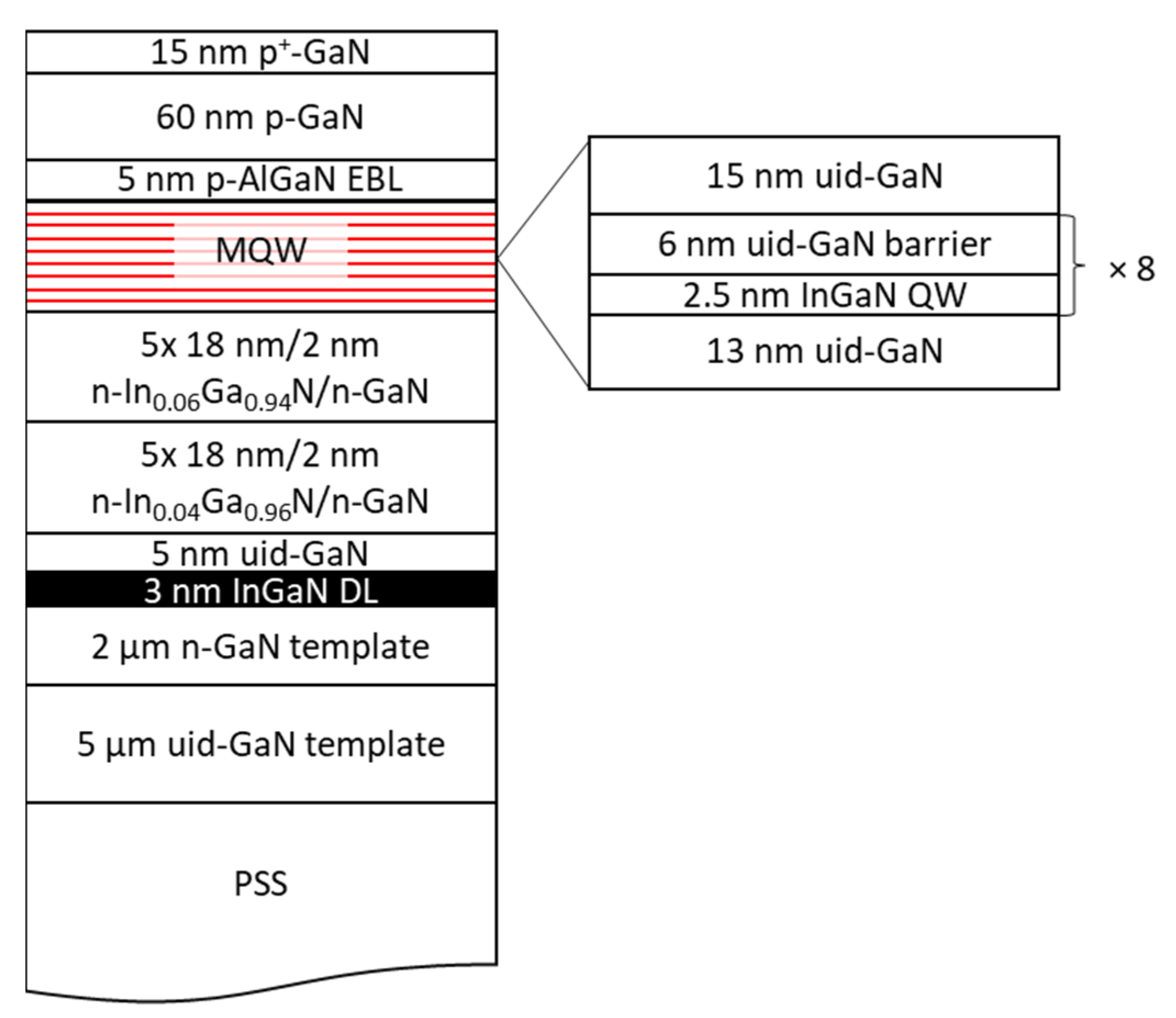
2. Materials and Methods

Similar growth of the LED epitaxial structure on SRTs has been reported previously [14,15]. The LED epitaxial structure on SRT is shown in Figure 1. The epitaxial structure was grown on patterned sapphire substrate with a 7.5 µm thick GaN template. First, a 3 nm InGaN decomposition layer was grown at 720 °C and this layer was capped with a 2.5 nm UID GaN at 720 °C, and 2.5 nm UID GaN at 825 °C. After that, two sets of InGaN superlattices (SLs) were grown. The two sets of SLs consisted of five periods of 18 nm n-In0.04Ga0.96N or n-In0.06Ga0.94N and 2 nm GaN at 930 °C and 920 °C, respectively. During the higher temperature growth of 930 °C, the decomposition layer thermally decomposed to form voids. The first set of SLs was referred to as the decomposition stop layer (DSL) and the second set of SLs served as the InGaN buffer. The developments and the corresponding relaxations of the decomposition layer, DSL, and SLs have been reported [14,15]. The active region was grown at 835 °C with eight periods of 2.5 nm InGaN/6 nm GaN quantum wells. Lastly, 5 nm of p-Al0.1Ga0.9N electron blocking layer (EBL), 60 nm p-GaN, and 15 nm p+-GaN were grown at 920 °C. The relatively thin p-Al0.1Ga0.9N EBL was attributed to the potential relaxation of the thicker AlGaN layer by growing on a higher lattice template. After the epitaxial growth, seven device sizes ranging from 5 × 5 to 100 × 100 µm2 were fabricated with 110 nm indium–tin oxide (ITO) contact and atomic layer deposition (ALD) for sidewall passivation; the details of the device fabrication and device designs have been reported in the literature [16,17]. On-wafer measurements were performed to obtain the electrical characteristics and packaging was executed to determine the optical and efficiency performances [18].

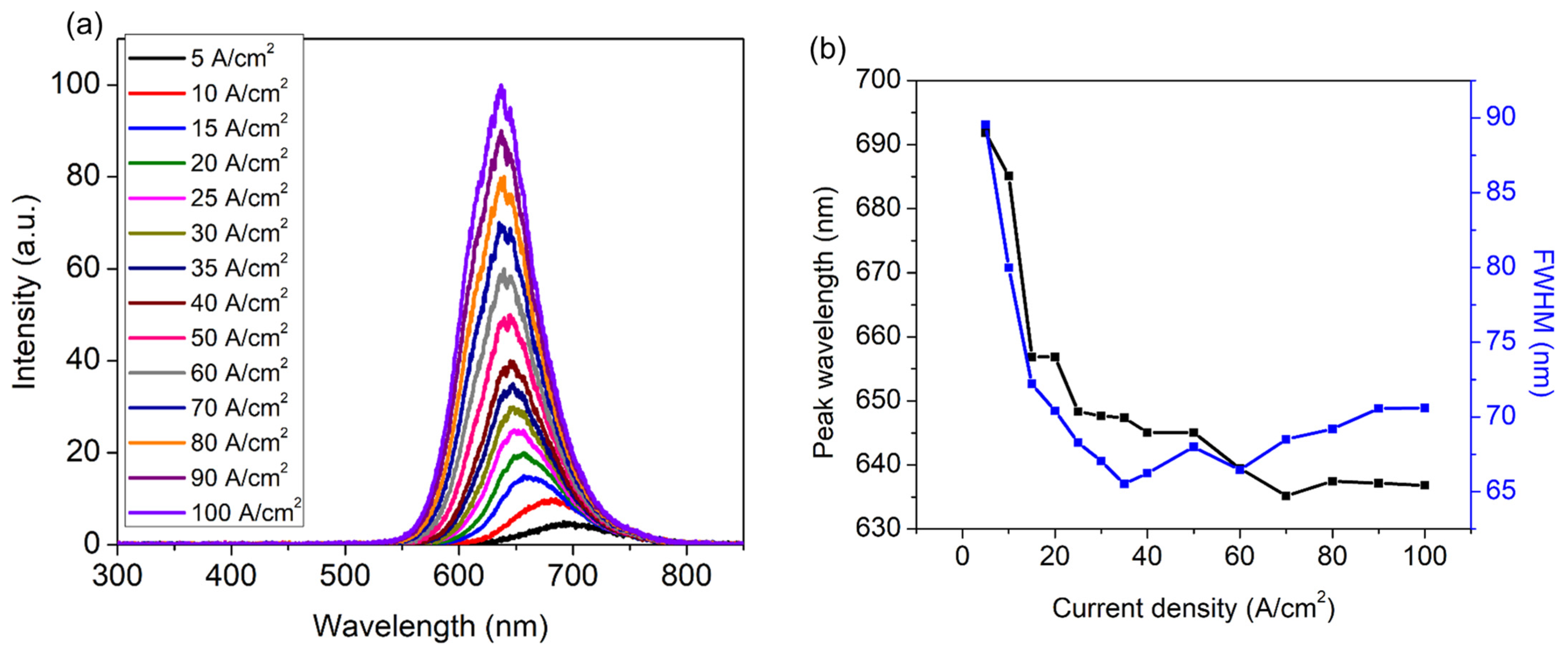
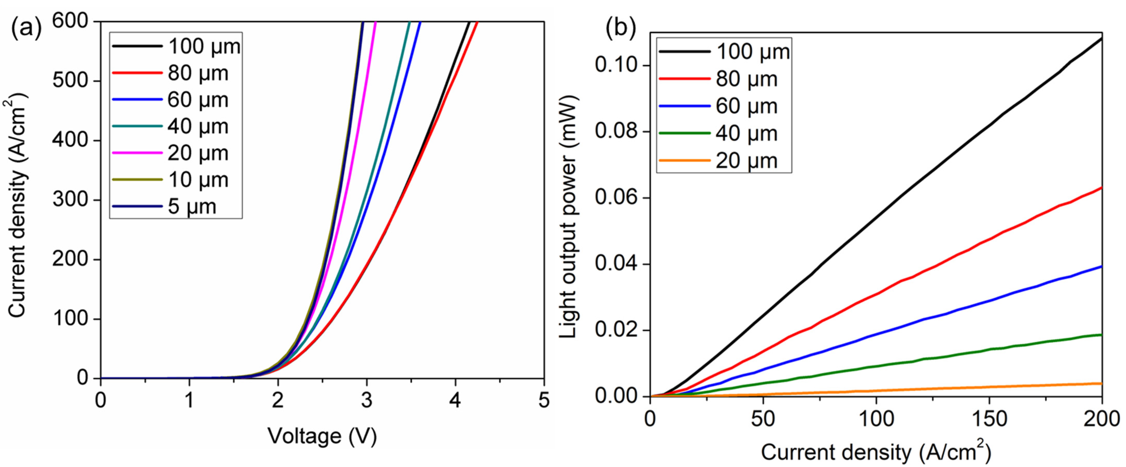
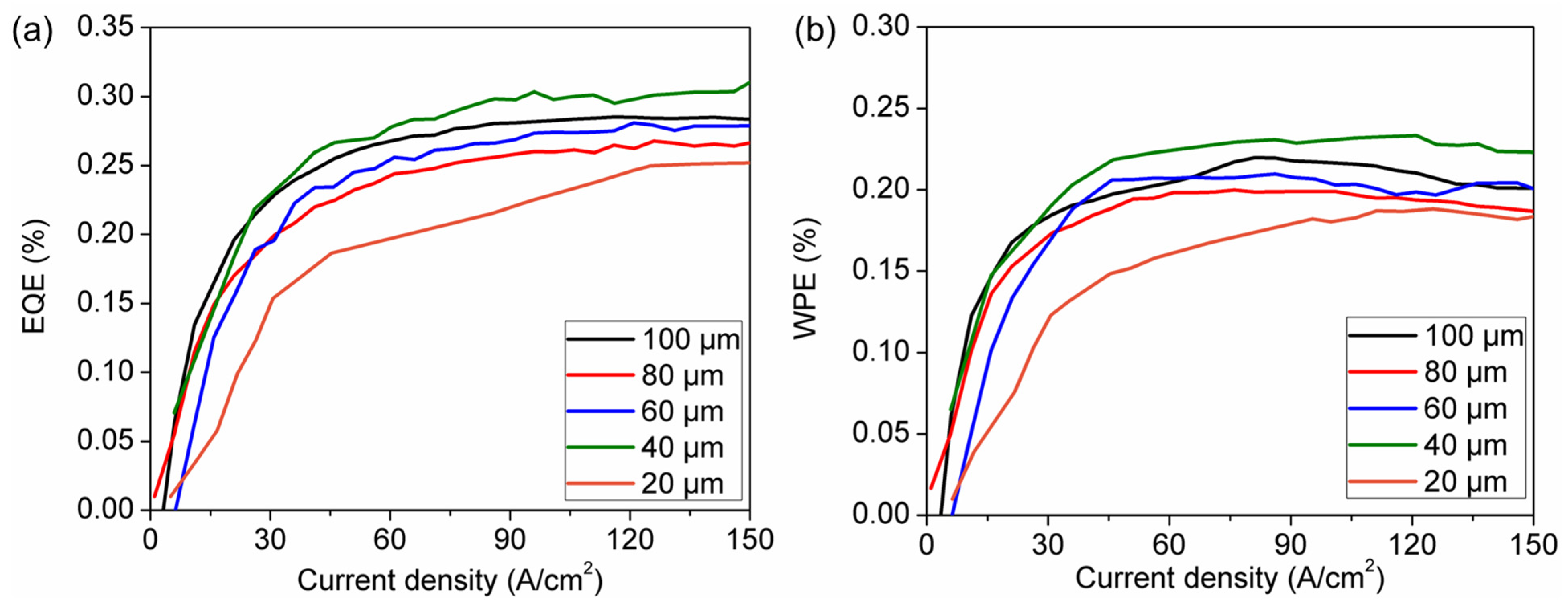
3. Results and Discussion

The emission spectra of a 100 × 100 µm2 device at different current density ranges and the corresponding peak wavelengths and FWHMs are shown in Figure 2a,b. The device yielded a blueshift of 55 nm in the peak wavelength, varying from 692 nm at 5 A/cm2 to 637 nm at 100 A/cm2. The blueshift in the peak wavelength was due to the quantum-confined Stark effect (QCSE) attributed to the charge screening of the polarization-related electric field in the quantum wells, where the degree of blueshift is similar to other c-plane GaN red LEDs [19,20]. The blueshift in the peak wavelength was also due to the large polarization-related electric field; c-plane polar orientation has the highest polarization-related electric field and lessens in semipolar and nonpolar crystal orientations [21,22]. To reduce or mitigate the effects of the polarization-induced electric field in the c-plane polar orientation, the use of polarization screening in the quantum wells by employing doped barriers is a promising option [23]. The peak wavelength variation was 15 nm across the two-inch wafer, from 639 nm to 654 nm, at 100 A/cm2. Additionally, the spectra did not show a separated blue emission at about 430–475 nm, suggesting that the InGaN active region did not show detrimental phase separation or alternately hole injection into the underlying InGaN/GaN SLs [10,24]. Nevertheless, the FWHM was very broad for display applications, and decreased from 90 nm at 5 A/cm2 to 66 nm at 35 A/cm2 and increased gradually to 70 nm at 100 A/cm2. For InGaN-based LEDs, the FWHM generally increased with wavelength emission due to indium fluctuation in the active region [9]. The reduction in electroluminescent FWHM from 5 to 35 A/cm2 could be due to emission from delocalized band states, while the increase in FWHM at higher current densities could be attributed to bandgap normalization due to an increase in junction temperature or excited states [24,25]. When increasing the current density, the color quality was affected by the screening of the internal electric field in the quantum wells, which drove the emission color from deep red towards red. One way to reduce the FWHM is to employ various color filters or reflectors to improve the InGaN red color quality, compared to the emission spectrum of AlGaInP red emitters [26,27]. Therefore, further growth optimizations are required to reduce the FWHM and to suppress the wavelength blueshift due to QCSE in c-plane InGaN red µLEDs.
The InGaN red devices yielded exceptional electrical and optical performances, including low forward voltage and relatively high light output power (LOP) characteristics. Figure 3a shows the current density–voltage characteristics of the µLEDs. All the devices yielded a low forward voltage, showing voltage values between 2.00 V and 2.05 V at 20 A/cm2, which is the lowest voltage characteristic compared to other InGaN red emitters in the literature [9,15,19,28,29,30]. The low voltage could be attributed to the better hole injection via v-defects in the active region, where the v-defects could be generated from the buffer layer surface with deep pits [14,15,19]. As the current density increased, the voltage performance was dominated by the current spreading in the devices, where larger devices resulted in higher resistive characteristics due to greater p-GaN areas [31]. Figure 3b presents the LOP–current density characteristics of the red devices. Although the LOP remained lower compared to the conventional planar growth approaches, the performance was better when comparing to the other relaxation methods, suggesting that the SRT method is promising to realize biaxially relaxed templates for red InGaN µLEDs [19,24,29,30].
The EQE and WPE characteristics are shown in Figure 4. The peak EQE and WPE were 0.31% and 0.21%, respectively, and the efficiency performance was weakly dependent on the device dimensions. The EQE and WPE curves were low and did not show significant droop behavior, indicating the efficiency performance was constrained by the material quality in the active region [32]. Efficiency limitation was likely due to the trap-assisted Auger recombination (TAAR), since the EQE was low and the curves did not reach a peak value. The internal quantum efficiency could be limited by the ratio of TAAR and the radiative recombination if TAAR plays a significant role, resulting in low efficiency without droop [32,33]. In addition to the low efficiency, the devices did not show detectable light emission for applied current densities less than 5 A/cm2. This indicates that the device performance was hindered by the defects in the active region; the Shockley–Read–Hall non-radiative recombination reduced radiative recombination at low current densities and TAAR prohibited the optimal efficiency at high current densities [6,32]. Hence, further optimizations in the active region should be performed, such as incorporating an AlGaN capping layer in the active region [24].

4. Conclusions

In conclusion, InGaN red µLEDs with low forward voltage characteristics were demonstrated in this study by employing the SRT method. The forward voltage values ranged between 2.00 V and 2.05 V at 20 A/cm2, which are the lowest among all red InGaN devices reported in the literature. The devices emitted at 692 nm at 5 A/cm2 and shifted to 637 nm at 100 A/cm2 due to the QCSE. The devices yielded higher LOP performance than other relaxation methods. Since the devices showed low efficiency due to defects and non-radiative centers in the active region, further material improvements are needed to create red InGaN µLEDs with high efficiency using the SRT method.

Author Contributions

Formal analysis, M.S.W. and P.C.; investigation, M.S.W.; resources, N.L., R.C.W. and H.Z.; writing—original draft preparation, M.S.W.; writing—review and editing, P.C., N.L., R.C.W. and H.Z.; supervision, S.N. and S.P.D.; project administration, S.N., S.P.D. and J.S.S.; funding acquisition, S.N., S.P.D. and J.S.S. All authors have read and agreed to the published version of the manuscript.

Funding

This work was funded by the Solid-State Lighting and Energy Electronics Center (SSLEEC) at the University of California, Santa Barbara (UCSB) and the Defense Advanced Research Project (DARPA), U.S. Department of Defense, under Grant No. HR00120C0135. J.S.S. would like to thank the support from the U.S. DOE EERE (grant # DE-EE0009691).

Institutional Review Board Statement

Not applicable.

Informed Consent Statement

Not applicable.

Data Availability Statement

Results presented in this paper are not available publicly at this time but may be obtained from the authors upon reasonable request.

Conflicts of Interest

The authors declare no conflict of interest.

References

  1. Huang, Y.; Hsiang, E.L.; Deng, M.Y.; Wu, S.T. Mini-LED, Micro-LED and OLED displays: Present status and future perspectives. Light Sci. Appl. 2020, 9, 105. [Google Scholar] [CrossRef] [PubMed]
  2. Wierer, J.J.; Tansu, N. III-Nitride Micro-LEDs for Efficient Emissive Displays. Laser Photon. Rev. 2019, 13, 1900141. [Google Scholar] [CrossRef]
  3. Jung, T.; Choi, J.H.; Jang, S.H.; Han, S.J. Review of Micro-light-emitting-diode Technology for Micro-display Applications. SID Symp. Dig. Tech. Pap. 2019, 50, 442–446. [Google Scholar] [CrossRef]
  4. Robin, Y.; Hemeret, F.; D’Inca, G.; Pristovsek, M.; Trassoudaine, A.; Amano, H. Monolithic integration of tricolor micro-LEDs and color mixing investigation by analog and digital dimming. Jpn. J. Appl. Phys. 2019, 58, SCCC06. [Google Scholar] [CrossRef]
  5. Wong, M.S.; Nakamura, S.; DenBaars, S.P. Review—Progress in High Performance III-Nitride Micro-Light-Emitting Diodes. ECS J. Solid State Sci. Technol. 2020, 9, 015012. [Google Scholar] [CrossRef]
  6. Wong, M.S.; Lee, C.; Myers, D.J.; Hwang, D.; Kearns, J.A.; Li, T.; JSpeck, S.; Nakamura, S.; DenBaars, S.P. Size-independent peak efficiency of III-nitride micro-light-emitting-diodes using chemical treatment and sidewall passivation. Appl. Phys. Express 2019, 12, 097004. [Google Scholar] [CrossRef]
  7. Wong, M.S.; Nakamura, S.; DenBaars, S.P. High External Quantum Efficiency III-Nitride Micro-Light-Emitting Diodes, 1st ed.; Elsevier Inc.: Amsterdam, The Netherlands, 2021; Volume 106. [Google Scholar]
  8. Pasayat, S.S.; Gupta, C.; Wong, M.S.; Wang, Y.; Nakamura, S.; Denbaars, S.P.; Keller, S.; Mishra, U.K. Growth of strain-relaxed InGaN on micrometer- sized patterned compliant GaN pseudo-substrates. Appl. Phys. Lett. 2020, 116, 111101. [Google Scholar] [CrossRef]
  9. White, R.C.; Khoury, M.; Wong, M.S.; Li, H.; Lynsky, C.; Iza, M.; Keller, S.; Sotta, D.; Nakamura, S.; DenBaars, S.P. Realization of iii-nitride c-plane microleds emitting from 470 to 645 nm on semi-relaxed substrates enabled by v-defect-free base layers. Crystals 2021, 11, 1168. [Google Scholar] [CrossRef]
  10. Iida, D.; Zhuang, Z.; Kirilenko, P.; Velazquez-Rizo, M.; Najmi, M.A.; Ohkawa, K. 633-nm InGaN-based red LEDs grown on thick underlying GaN layers with reduced in-plane residual stress. Appl. Phys. Lett. 2020, 116, 162101. [Google Scholar] [CrossRef]
  11. Even, A.; Laval, G.; Ledoux, O.; Ferret, P.; Sotta, D.; Guiot, E.; Levy, F.; Robin, I.C.; Dussaigne, A. Enhanced in incorporation in full InGaN heterostructure grown on relaxed InGaN pseudo-substrate. Appl. Phys. Lett. 2017, 110, 262103. [Google Scholar] [CrossRef]
  12. El-Ghoroury, H.; Nakajima, Y.; Yeh, M.; Liang, E.; Chuang, C.-L.; Chen, J.C. Color temperature tunable white light based on monolithic color-tunable light emitting diodes. Opt. Express 2020, 28, 1206–1215. [Google Scholar] [CrossRef] [PubMed]
  13. White, R.C.; Li, H.; Khoury, M.; Lynsky, C.; Iza, M.; Keller, S.; Sotta, D.; Nakamura, S.; DenBaars, S.P. InGaN-Based microLED Devices Approaching 1% EQE with red 609 nm Electroluminescence on Semi-Relaxed Substrates. Crystals 2021, 11, 1364. [Google Scholar] [CrossRef]
  14. Chan, P.; DenBaars, S.P.; Nakamura, S. Growth of highly relaxed InGaN pseudo-substrates over full 2-in. wafers. Appl. Phys. Lett. 2021, 119, 131106. [Google Scholar] [CrossRef]
  15. Chan, P.; Rienzi, V.; Lim, N.; Chang, H.M.; Gordon, M.; DenBaars, S.P.; Nakamura, S. Demonstration of relaxed InGaN-based red LEDs grown with high active region temperature. Appl. Phys. Express 2021, 14, 101002. [Google Scholar] [CrossRef]
  16. Wong, M.S.; Hwang, D.; Alhassan, A.I.; Lee, C.; Ley, R.; Nakamura, S.; DenBaars, S.P. High Efficiency of III-Nitride Micro-Light-Emitting Diodes by Sidewall Passivation Using Atomic Layer Deposition. Opt. Express 2018, 26, 21324–21331. [Google Scholar] [CrossRef]
  17. Hwang, D.; Mughal, A.J.; Wong, M.S.; Alhassan, A.I.; Nakamura, S.; Denbaars, S.P. Micro-light-emitting diodes with III-nitride tunnel junction contacts grown by metalorganic chemical vapor deposition. Appl. Phys. Express 2018, 11, 012102. [Google Scholar] [CrossRef]
  18. Wong, M.S.; Oh, S.H.; Back, J.; Lee, C.; Speck, J.S.; Nakamura, S.; DenBaars, S.P. Enhanced external quantum efficiency of III-nitride micro-light-emitting diodes using vertical and transparent package. Jpn. J. Appl. Phys. 2021, 60, 020905. [Google Scholar] [CrossRef]
  19. Iida, D.; Zhuang, Z.; Kirilenko, P.; Velazquez-Rizo, M.; Ohkawa, K. Demonstration of low forward voltage InGaN-based red LEDs. Appl. Phys. Express 2020, 13, 031001. [Google Scholar] [CrossRef]
  20. Zhuang, Z.; Iida, D.; Ohkawa, K. Effects of size on the electrical and optical properties of InGaN-based red light-emitting diodes. Appl. Phys. Lett. 2020, 116, 173501. [Google Scholar] [CrossRef]
  21. Feezell, D.F.; Speck, J.S.; Denbaars, S.P.; Nakamura, S. Semipolar (2021) InGaN/GaN light-emitting diodes for high-efficiency solid-state lighting. IEEE/OSA J. Disp. Technol. 2013, 9, 190–198. [Google Scholar] [CrossRef]
  22. Young, N.G.; Farrell, R.M.; Oh, S.; Cantore, M.; Wu, F.; Nakamura, S.; DenBaars, S.P.; Weisbuch, C.; Speck, J.S. Polarization field screening in thick (0001) InGaN/GaN single quantum well light-emitting diodes. Appl. Phys. Lett. 2016, 108, 061105. [Google Scholar] [CrossRef]
  23. Chow, Y.C.; Lynsky, C.; Wu, F.; Nakamura, S.; DenBaars, S.P.; Weisbuch, C.; Speck, J.S. Reduction of efficiency droop in c-plane InGaN/GaN light-emitting diodes using a thick single quantum well with doped barriers. Appl. Phys. Lett. 2021, 119, 221102. [Google Scholar] [CrossRef]
  24. Hwang, J.-I.; Hashimoto, R.; Saito, S.; Nunoue, S. Development of InGaN-based red LED grown on (0001) polar surface. Appl. Phys. Express 2014, 7, 071003. [Google Scholar] [CrossRef]
  25. Funato, M.; Ueda, M.; Kawakami, Y.; Narukawa, Y.; Kosugi, T.; Takahashi, M.; Mukai, T. Blue, green, and amber InGaN/GaN light-emitting diodes on semipolar {1122} GaN bulk substrates. Jpn. J. Appl. Phys. 2006, 45, L659. [Google Scholar] [CrossRef]
  26. Wong, M.S.; Kearns, J.A.; Lee, C.; Smith, J.M.; Lynsky, C.; Lheureux, G.; Choi, H.; Kim, J.; Kim, C.; Nakamura, S.; et al. Improved performance of AlGaInP red micro-light-emitting diodes with sidewall treatments. Opt. Express 2020, 28, 5787–5793. [Google Scholar] [CrossRef]
  27. Chen, G.; Wei, B.; Lee, C.; Lee, H. Monolithic Red/Green/Blue Micro-LEDs with HBR and DBR Structures. IEEE Photonics Technol. Lett. 2018, 30, 262–265. [Google Scholar] [CrossRef]
  28. Pasayat, S.S.; Ley, R.; Gupta, C.; Wong, M.S.; Lynsky, C.; Wang, Y.; Gordon, M.J.; Nakamura, S.; Denbaars, S.P.; Keller, S.; et al. Color-tunable <10 μ m square InGaN micro- LEDs on compliant GaN-on-porous-GaN. Appl. Phys. Lett. 2020, 117, 061105. [Google Scholar]
  29. Li, P.; Li, H.; Zhang, H.; Lynsky, C.; Iza, M.; Speck, J.S.; Nakamura, S.; DenBaars, S.P. Size-independent peak external quantum efficiency (>2%) of InGaN red micro-light-emitting diodes with an emission wavelength over 600 nm. Appl. Phys. Lett. 2021, 119, 081102. [Google Scholar] [CrossRef]
  30. Pasayat, S.S.; Gupta, C.; Wong, M.S.; Ley, R.; Gordon, M.J.; DenBaars, S.P.; Nakamura, S.; Keller, S.; Mishra, U.K. Demonstration of ultra-small (<10 μm) 632 nm red InGaN micro-LEDs with useful on-wafer external quantum efficiency (>0.2%) for mini-displays. Appl. Phys. Express 2021, 14, 011004. [Google Scholar] [CrossRef]
  31. Hwang, D.; Mughal, A.; Pynn, C.D.; Nakamura, S.; DenBaars, S.P. Sustained high external quantum efficiency in ultrasmall blue III-nitride micro-LEDs. Appl. Phys. Express 2017, 10, 032101. [Google Scholar] [CrossRef]
  32. Myers, D.J.; Espenlaub, A.C.; Gelzinyte, K.; Young, E.C.; Martinelli, L.; Peretti, J.; Weisbuch, C.; Speck, J.S. Evidence for trap-assisted Auger recombination in MBE grown InGaN quantum wells by electron emission spectroscopy. Appl. Phys. Lett. 2020, 116, 091102. [Google Scholar] [CrossRef]
  33. Espenlaub, A.C.; Myers, D.J.; Young, E.C.; Marcinkevičius, S.; Weisbuch, C.; Speck, J.S. Evidence of trap-assisted Auger recombination in low radiative efficiency MBE-grown III-nitride LEDs. J. Appl. Phys. 2019, 126, 184502. [Google Scholar] [CrossRef]
Figure 1. Schematic of the LED epitaxial design.
Crystals 12 00721 g001
Figure 2. (a) Emission spectra from 5 to 100 A/cm2 from a 100 × 100 µm2 device and (b) the peak wavelength and FWHM with current densities from the 100 × 100 µm2 device.
Crystals 12 00721 g002
Figure 3. (a) Current density–voltage characteristics and (b) LOP–current density characteristics of the packaged red InGaN devices.
Crystals 12 00721 g003
Figure 4. The dependence of (a) EQE and (b) WPE with the current density of packaged red InGaN devices.
Crystals 12 00721 g004
Publisher’s Note: MDPI stays neutral with regard to jurisdictional claims in published maps and institutional affiliations.

