
Crystal Growth and Characterization of ZrSiS-Type Topological Dirac Semimetals
by

Ying Yang
1,2, 
Peng Zhu
1,2,3,
Liu Yang
1,2,
Jinjin Liu
1,2,
Yongkai Li
1,2,3 and
Zhiwei Wang
1,2,3,* 1
Key Laboratory of Advanced Optoelectronic Quantum Architecture and Measurement, Ministry of Education, School of Physics, Beijing Institute of Technology, Beijing 100081, China
2
Micronano Centre, Beijing Key Lab of Nanophotonics & Ultrafine Optoelectronic Systems, Beijing Institute of Technology, Beijing 100081, China
3
Material Science Center, Yangtze Delta Region Academy of Beijing Institute of Technology, Jiaxing 314011, China
*
Author to whom correspondence should be addressed.
Crystals 2022, 12(5), 728; https://0-doi-org.brum.beds.ac.uk/10.3390/cryst12050728
Submission received: 19 April 2022
/
Revised: 16 May 2022
/
Accepted: 17 May 2022
/
Published: 19 May 2022
(This article belongs to the Section Inorganic Crystalline Materials)
Abstract
:WHM materials (W = Zr/Hf, H = Si/Ge/Sn, M = S/Se/Te) represent a large family of topological semimetals, which have attracted intensive interest since they are considered to be good candidates for studying various topological states. Here, we report the crystal growth, characterization, and electronic properties of HfSiS, ZrGeS, and ZrGeSe. All samples were prepared by a chemical vapor transport method with I2 as a transport agent, and the growth conditions were optimized. X-ray diffraction (XRD) measurements showed that the as-grown crystals crystallized in a PbFCl-type layered structure. They all showed metallic behavior from temperature-dependent resistivity measurements and the carrier densities were estimated to be in the order of 1021 cm−3. A large magnetoresistance of up to 1200% and an obvious Shubnikov–de Hass (SdH) oscillation were observed for HfSiS.
1. Introduction
Topological semimetals represent new topological states of quantum matter and exhibit a variety of exotic properties, such as extremely high carrier mobility [1,2,3,4], large magnetoresistance (MR) [5,6,7,8,9], chiral anomaly [10,11], and potential topological superconductivity [12], which have tremendous potential applications in the future. According to the way the valance band and the conduction band touch each other, we can classify topological semimetals into Dirac semimetals, Weyl semimetals, nodal-line semimetals, and so on. Na3Bi [9,10] and Cd3As2 [11,12,13,14] are two kinds of widely-investigated Dirac semimetals. In a Dirac semimetal, there are fourfold degenerate linear band crossings at the Dirac nodes, which are protected by their crystal symmetry. Once the spin degeneracy is separated by time-reversal symmetry breaking or crystal symmetry breaking, a Dirac semimetal can transform into a Weyl semimetal, in which the Dirac cone splits to a pair of Weyl cones that have opposite chirality [9,11,15,16]. The inversion symmetry breaking Weyl semimetal has been realized in the TaAs-type family [15,16,17] and the WTe2/MoTe2 family [18,19,20], while the spontaneous time-reversal symmetry breaking Weyl semimetal has been reported in YbMnBi2 [21], magnetic Heusler alloys [22], RAlX (R = rare earth, X = Si, Ge) compounds [23], Co3Sn2S2 [24], and so on.
The Dirac/Weyl nodes in the above topological semimetals are discrete in the momentum space. However, there is another novel type of topological semimetal (called topological nodal-line semimetal), which was predicted to host a one-dimensional nodal line or loop at its band crossing [25,26,27,28]. Nodal-line semimetals are experimentally observed in several kinds of materials such as PbTaSe2 [29], PtSn4 [30], and ZrSiM (M = S, Se, Te) [31,32,33,34,35]. Among these materials, the layered material ZrSiM, which belongs to the WHM-family material with a PbFCl-type structure, attracted more intensive interests due to its unique properties. The electronic band structures of the WHM-family materials with different combinations of W, H, and M elements are very similar and all of them present nodal-line states, except for some small discrepancies due to their different spin–orbit coupling (SOC) strength and structural dimensionality [27]. Actually, the ZrSiM nodal-line semimetal systems are widely studied and demonstrated by ARPES [32], STM [35], quantum oscillations [36], infrared spectra [37], and so on. Since SOC strength and structural dimensionality can be tuned by combining different elements of W, H, and M, the WHM materials provide a good opportunity to investigate the interplay between SOC and nonsymmorphic symmetry. However, although the crystal growth and novel physical properties of the WHM-family materials have been studied intensively [38,39,40,41], there are a few studies on the optimization of the crystal growth conditions of this kind of materials. As we know, WHM materials are very suitable for quantum device fabrications and investigations because of their layered structure feature. However, first, large-size single crystals with high quality are needed for exfoliation. In this study, we reported the optimized crystal growth and electronic transport characterization of HfSiS, ZrGeS, and ZrGeSe.
2. Materials and Methods
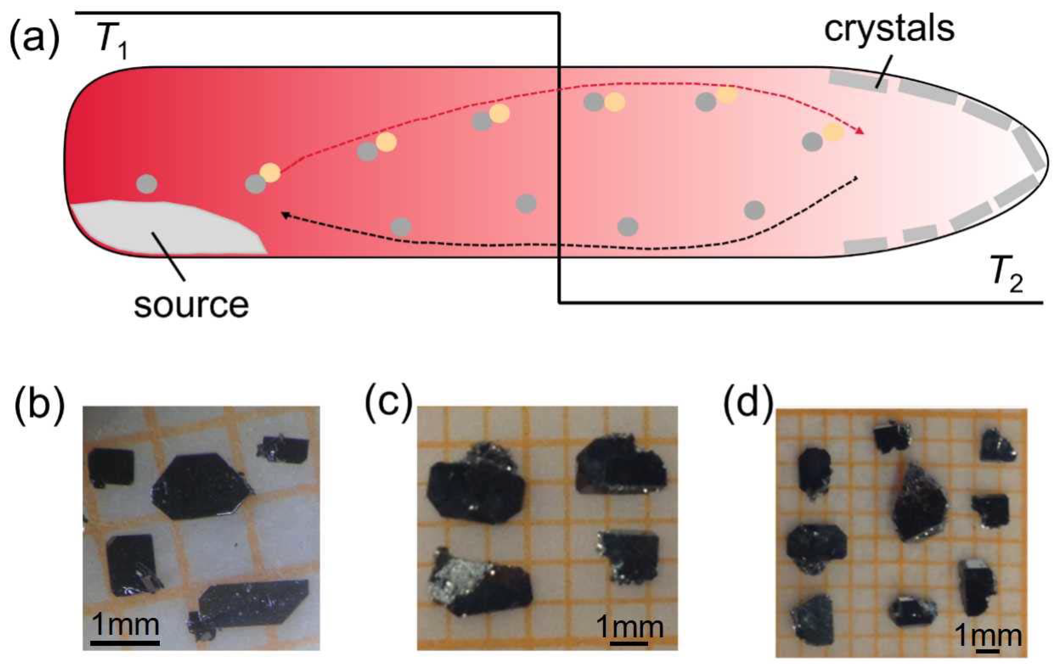
High-quality WHM (W = Hf and Zr, H = Si and Ge, M = S and Se) single crystals were grown by a chemical vapor transport method using I2 as a transport agent. High-purity Zr or Hf powder (99.8%), Si or Ge powder (99.999%), S pieces (99.999%), or Se shot (99.999%) are used as the starting materials. To obtain high-quality crystals, pretreatment of the starting materials (Zr, Hf and Se) was performed to remove possible oxide layers on their surfaces, as described elsewhere [42,43]. Specifically, the above-mentioned starting materials were sealed in a quartz tube with hydrogen of 0.8 atm individually, and then, they were annealed for 10 h at 873 K for Zr and Hf and 450 K for Se, respectively. This pretreatment process is quite important to obtain large crystals with high quality. After that, the starting material, with a total mass of 1g, is weighed with a molar ratio of W:H:M = 1:1:1 and sealed in an evacuated quartz tube (16 cm in length and 8 mm in inner diameter, with a base pressure lower than 2 × 10⁻⁴ Pa). Each tube was sealed together with 40 mg I2 pieces (99.99%); the I2 concentration is about 5 µg/mL. Then, the quartz tubes were placed horizontally in a two-zone tube furnace with a temperature gradient set to 100 K. The source materials were placed on the hot side, as shown in Figure 1a. The hot side of the furnace was heated slowly to 1373 K for HfSiS and 1153 K for ZrGeS and ZrGeSe. After it was kept on for 2 weeks, the furnace was cooled down to room temperature with the power shut down. Shiny crystals with rectangular features were obtained, as shown in Figure 1b–d. Actually, we have tried several growths of the above three materials under different growth conditions and found the above conditions to be the optimal conditions for obtaining large-size single crystals.
The structure was characterized by XRD using a Bruker D8 Advance X (Karlsruhe, Germany) with Cu-Kα radiation. The chemical compositions of the as-grown single crystals were identified using a scanning electron microscope (SEM, JEOL JSM-7500F, Tokyo, Japan) equipped with energy-dispersive X-ray spectroscopy (EDX, Oxford Instruments, Oxford, UK). Electronic transport measurements were carried out on a physical property measurement system (PPMS, Quantum Design, San Diego, CA, USA) at a temperature down to 1.8 K and a magnetic field within ±9 T. Gold wires were used to connect the samples by a room temperature-cured silver paste to make ohmic contacts.
3. Results and Discussion
WHM-family materials crystallize in a layered structure, which is similar to PbFCl, as illustrated in Figure 2a. A Zr/Hf atom is coordinated by four Si/Ge and four S/Se atoms, while Si/Ge and S/Se atoms are arranged in square planes. Within a layer, the atoms are stacked as S/Se–Zr/Hf–Si/Ge–Zr/Hf–S/Se along the c-axis. The distance between each layer, i.e., the lattice parameter of c, becomes larger and larger when an M atom changes from S to Te. Figure 2b shows the XRD patterns of HfSiS, ZrGeS and ZrGeSe single crystals. The sharp diffraction peaks indicate good crystallinity of our single crystals. We can only observe (001) peaks which can be easily indexed according to their tetragonal structures with a space group P4/nmm. The lattice parameters of c can be calculated as follows: 7.995 Å, 8.018 Å, and 8.269 Å for HfSiS, ZrGeS, and ZrGeSe, respectively.
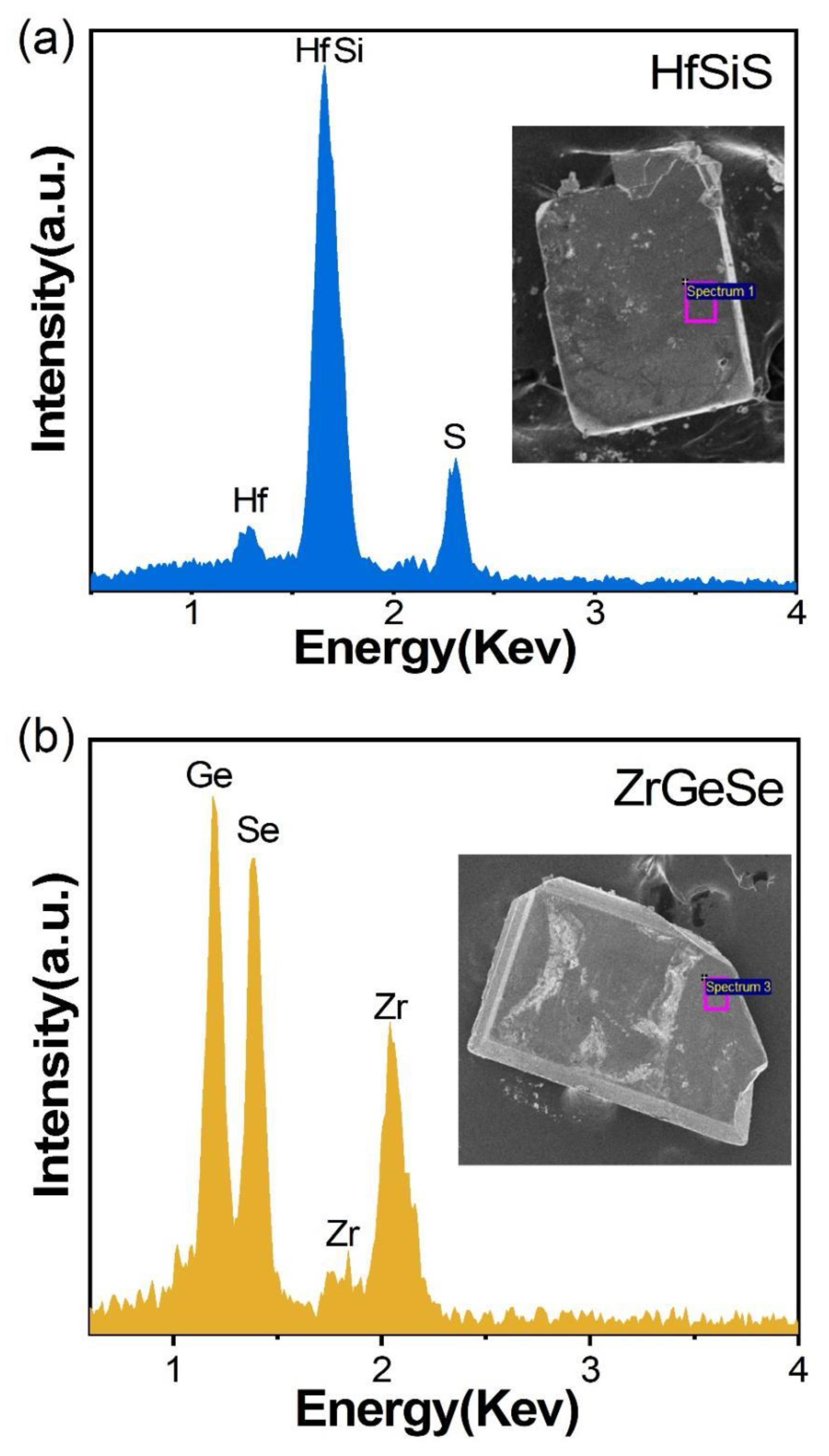
To check the chemical composition of the as-grown crystals, we performed energy-dispersive X-ray spectroscopy (EDS) measurements for HfSiS and ZrGeSe, as shown in Figure 3. We can see that each sample presents its own corresponding three elements. In HfSiS, the peaks of the Hf M-line (1.645 eV) and Si L-line (1.740 eV) almost overlap since their energy is quite close to each other; we can still roughly obtain the composition as follows: Hf:Si:S = 34.6:34.6:30.8. This indicates that there is a certain S vacancy in the HfSiS crystal. This seems quite common in sulfides since the S is very easy to evaporate during growth at high temperature. In contrast, the composition for ZrGeSe is estimated to be as follows: Zr:Ge:Se = 32.9:33.0:34.1, which is very close to the nominal composition. The insets of each panel show SEM images of both crystals, which presents a tetragonal structure feature.
Figure 4 presents the electronic transport properties of HfSiS. From the ρxx (T) curve, as shown in Figure 4a, we can see that the resistivity decreases with the temperature cooling down, indicating a metallic behavior. The residual resistivity ρ0 is about 3.5 μΩ cm and the residual resistivity ratio (RRR) is calculated to be about 14, which implies the high quality of the crystal. Figure 4b shows the magnetic field dependence of the Hall resistivity ρyx (B), measured at 2 K. A slightly nonlinear ρyx (B) behavior suggests the existence of two or more bands at the Fermi level. In addition, the positive slope of the ρyx (B) curve indicates that the dominate carrier is a p-type, (i.e., holes), and we can obtain an approximate carrier density p of about 2.3 × 1021 cm−3 from the slope at low fields.
Figure 4c presents the magnetic field dependence of the magnetoresistance (MR) of HfSiS at 2 K with an applied field from −9 T to 9 T. We can see that the MR reaches 1200% with a magnetic field of up to 9 T. It is quite common that a Dirac semimetal shows a very large MR, such as in WTe2, ZrSiS, etc. [27,44]. However, this large MR cannot be explained with the mobility we extracted above. According to the formula of classical magnetoresistance , where , , and are the resistivity at the zero field, carrier mobility, and applied magnetic field, respectively. We can get a mobility of about 3900 cm2/Vs. From the field dependence of MR, we can see a clear Shubnikov–de Hass (SdH) oscillation when the magnetic field is applied higher than 6 T. This result is similar to that reported by Delft et al. [45]. Figure 4d shows the quantum oscillations in dρyx/dB, in which the main oscillation frequency F is 285 T and the corresponding hole density (assuming a spherical Fermi surface) is 2.7 × 1019 cm−3. We can see that the carrier density obtained from the SdH oscillation is lower than that from the Hall measurement. One of the possible reasons for this discrepancy is that HfSiS actually has multiple Fermi surfaces, as reported by Delft et al. [45], and our carrier density calculation from the Hall data will introduce some overestimations. Another possible reason is that the carrier density estimated from the SdH oscillation corresponds to the specific band which related to this oscillation; it cannot reflect the exact carrier density of the material which features multibands.
We also characterized the electronic properties of ZrGeS and ZrGeSe and the results are shown in Figure 5. Obviously, both samples are metallic, as shown in Figure 5a,c. The residual resistivities are 4.8 μΩ cm with an RRR of 8.1 for ZrGeS and 11.7 μΩ cm with an RRR of 3.2 for ZrGeSe, respectively. There is a kink at about 30 K for ZrGeSe, which seems intrinsic because we can reproduce this kink during the cooling down and warming up processes. The origin of this kink is not clear at present; one possibility is that there is a phase transition, which we left for future studies. The Hall resistivity is quite similar to that of HfSiS and the ρyx (B) curves show to be slightly deviated from the linear, as shown in Figure 5b,d, suggesting at least two kinds of carriers. Multiple carrier behavior indicates there is more than one band at the Fermi level and this multiband feature was confirmed by the de Haas–van Alphen (dHvA) effect [40] and ARPES measurements [46]. However, the dominated carrier is hole and the carrier densities are estimated to be 5.4 × 1021 cm−3 for ZrGeS and 3.2 × 1021 cm−3 for ZrGeSe, where slopes at low fields are used. We also would like to point out that no SdH oscillation was observed in ZrGeS and ZrGeSe. This is probably because the Feimi levels of these two compounds are slightly further away from the Dirac nodal-line.
4. Conclusions
In summary, we have successfully grown HfSiS, ZrGeS, and ZrGeSe single crystals by a chemical vapor transport method and the optimal growth conditions have been found. All crystals crystallize in a layered PbFCl-structure. From the resistivity measurements, they all show metallic behavior. The main carrier is a hole and the carrier densities are in the order of 1021 cm−3. Besides, HfSiS has a very large MR, up to 1200%, and a clear SdH oscillation with an oscillation frequency of 285 T. ZrSiS-type Dirac semimetals are very interesting not only because they host a variety of novel topological features, but also, they are considered to be a good platform for the study of quantum devices because of their cleavability, due to a layered structure feature, as well as their stability against air. We hope our work can promote the development of quantum devices based on Dirac materials.
Author Contributions
Y.Y. grew the single crystals. Y.Y. and P.Z. performed XRD and SEM measurements and analysis. Y.Y., P.Z., L.Y., J.L. and Y.L. performed the transport measurement and analyzed the results. Writing—reviewing and editing: Z.W. All authors discussed the results and contributed to writing the manuscript. Z.W. conceived the project. All authors have read and agreed to the published version of the manuscript.
Funding
This work was supported by the National Natural Science Foundation of China (No. 92065109), Beijing Natural Science Foundation (Nos. Z210006 and Z190006), and Beijing Institute of Technology Research Fund Program for Young Scholars (No. 3180012222011).
Institutional Review Board Statement
Not applicable.
Informed Consent Statement
Not applicable.
Data Availability Statement
Data available in a publicly accessible repository.
Acknowledgments
Z.W. would like to thank Fan Yang at Tianjin University for helpful discussion. Z.W. thanks the Analysis &Testing Center at BIT for assistance in facility support.
Conflicts of Interest
The authors declare no conflict of interest.
References
- Yang, J.; Zhen, W.; Liang, D.; Wang, Y.; Zhang, C. Current jetting distorted planar hall effect in a Weyl semimetal with ultrahigh mobility. Phys. Rev. Mater. 2019, 3, 014201. [Google Scholar] [CrossRef] [Green Version]
- Wang, Z.; Zheng, Y.; Shen, Z.; Lu, Y.; Fang, H.; Sheng, F.; Zhou, Y.; Yang, X.; Li, Y.; Feng, C.; et al. Helicity protected ultrahigh mobility Weyl fermions in NbP. Phys. Rev. B 2016, 93, 121112. [Google Scholar] [CrossRef] [Green Version]
- Okamoto, Y.; Saigusa, K.; Wada, T.; Yamakawa, Y.; Yamakage, A.; Sasagawa, T.; Katayama, N.; Takatsu, H.; Kageyama, H.; Takenaka, K. High-mobility carriers induced by chemical doping in the candidate nodal-line semimetal CaAgP. Phys. Rev. B 2020, 102, 121112. [Google Scholar] [CrossRef]
- Hou, Z.; Wang, W.; Xu, G.; Zhang, X.; Wei, Z.; Shen, S.; Liu, E.; Yao, Y.; Chai, Y.; Sun, Y.; et al. High electron mobility and large magnetoresistance in the half-Heusler semimetal LuPtBi. Phys. Rev. B 2015, 92, 235134. [Google Scholar] [CrossRef] [Green Version]
- Feng, J.; Pang, Y.; Wu, D.; Wang, Z.; Weng, H.; Li, J.; Dai, X.; Fang, Z.; Shi, Y.; Lu, L. Large linear magnetoresistance in Dirac semimetal Cd3As2 with Fermi surfaces close to the Dirac points. Phys. Rev. B 2015, 92, 081306. [Google Scholar] [CrossRef] [Green Version]
- Yuan, Z.; Lu, H.; Liu, Y.; Wang, J.; Jia, S. Large magnetoresistance in compensated semimetals TaAs2 and NbAs2. Phys. Rev. B 2016, 93, 184405. [Google Scholar] [CrossRef] [Green Version]
- Shekhar, C.; Nayak, A.K.; Sun, Y.; Schmidt, M.; Nicklas, M.; Leermakers, I.; Zeitler, U.; Skourski, Y.; Wosnitza, J.; Liu, Z.; et al. Extremely large magnetoresistance and ultrahigh mobility in the topological Weyl semimetal candidate NbP. Nat. Phys. 2015, 11, 645–649. [Google Scholar] [CrossRef]
- Baibich, M.N.; Broto, J.M.; Fert, A.; NguyenVanDau, F.; Petroff, F.; Etienne, P.; Creuzet, G.; Friederich, A.; Chazelas, J. Giant magnetoresistance of (001)Fe/(001)Cr magnetic superlattices. Phys. Rev. Lett. 1988, 61, 2472–2475. [Google Scholar] [CrossRef] [Green Version]
- Wang, Z.; Sun, Y.; Chen, X.-Q.; Franchini, C.; Xu, G.; Weng, H.; Dai, X.; Fang, Z. Dirac semimetal and topological phase transitions in A3Bi (A = Na, K, Rb). Phys. Rev. B 2012, 85, 195320. [Google Scholar] [CrossRef] [Green Version]
- Xiong, J.; Kushwaha, S.; Liang, T.; Krizan, J.; Hirschberger, M.; Wang, W. Evidence for the chiral anomaly in the Dirac semimetal Na3Bi. Science 2015, 350, 413–416. [Google Scholar] [CrossRef] [Green Version]
- Jia, Z.; Li, C.; Li, X.; Shi, J.; Liao, Z.; Yu, D.; Wu, X. Thermoelectric signature of the chiral anomaly in Cd3As2. Nat. Mater. 2016, 7, 13013. [Google Scholar] [CrossRef] [PubMed]
- Wang, H.; Wang, H.; Liu, H.; Lu, H.; Yang, W.; Jia, S.; Liu, X.; Xie, X.C.; Wei, J.; Wang, J. Observation of superconductivity induced by a point contact on 3d dirac semimetal Cd3As2 crystals. Nat. Mater. 2016, 15, 38–42. [Google Scholar] [CrossRef] [PubMed]
- Liu, Z.; Jiang, J.; Zhou, B.; Wang, Z.; Zhang, Y.; Weng, H.; Prabhakaran, D.; Mo, S.-K.; Peng, H.; Dudin, P.; et al. A stable three-dimensional topological Dirac semimetal Cd3As2. Nat. Mater. 2014, 13, 677–681. [Google Scholar] [CrossRef] [PubMed]
- Jeon, S.; Zhou, B.; Gyenis, A.; Feldman, B.; Kimchi, I.; Potter, A.; Gibson, Q.; Cava, R.; Vishwanath, A.; Yazdani, A. Landau quantization and quasiparticle interference in the three-dimensional Dirac semimetal Cd3As2. Nat. Mater. 2014, 13, 851–856. [Google Scholar] [CrossRef] [PubMed] [Green Version]
- Huang, S.-M.; Xu, S.-Y.; Belopolski, I.; Lee, C.-C.; Chang, G.; Wang, B.; Alidoust, N.; Bian, G.; Neupane, M.; Zhang, C.; et al. A Weyl Fermion semimetal with surface Fermi arcs in the transition metal monopnictide TaAs class. Nat. Commun. 2015, 6, 7373. [Google Scholar] [CrossRef] [PubMed]
- Zhang, C.-L.; Tong, B.; Yuan, Z.; Lin, Z.; Wang, J.; Zhang, J.; Xi, C.-Y.; Wang, Z.; Jia, S.; Zhang, C. Signature of chiral fermion instability in the Weyl semimetal TaAs above the quantum limit. Phys. Rev. B 2016, 94, 250120. [Google Scholar] [CrossRef] [Green Version]
- Xu, S.-Y.; Alidoust, N.; Belopolski, I.; Yuan, Z.; Bian, G.; Chang, T.-R.; Zheng, H.; Strocov, V.N.; Sanchez1, D.S.; Chang, G.; et al. Discovery of a Weyl fermion state with Fermi arcs in niobium arsenide. Nat. Phys. 2015, 11, 748–754. [Google Scholar] [CrossRef] [Green Version]
- Wang, C.; Zhang, Y.; Huang, J.; Nie, S.; Liu, G.; Liang, A.; Zhang, Y.; Shen, B.; Liu, J.; Hu, C.; et al. Observation of Fermi arc and its connection with bulk states in the candidate type-II Weyl semimetal WTe2. Phys. Rev. B 2016, 94, 241119. [Google Scholar] [CrossRef] [Green Version]
- Wu, Y.; Mou, D.; Jo, N.H.; Sun, K.; Huang, L.; Bud’ko, S.L.; Canfield, P.C.; Kaminski, A. Observation of Fermi arcs in the type-II Weyl semimetal candidate WTe2. Phys. Rev. B 2016, 94, 121113. [Google Scholar] [CrossRef] [Green Version]
- Wang, Z.; Wieder, B.J.; Li, J.; Yan, B.; Bernevig, B.A. Higher-Order Topology, Monopole Nodal Lines, and the Origin of Large Fermi Arcs in Transition Metal Dichalcogenides XTe2 (X = Mo; W). Phys. Rev. Lett. 2019, 123, 186401. [Google Scholar] [CrossRef] [Green Version]
- Borisenko, S.; Evtushinsky, D.; Gibson, Q.; Yaresko, A.; Koepernik, K.; Kim, T.; Ali, M.; van den Brink, J.; Hoesch, M.; Fedorov, A.; et al. Time-reversal symmetry breaking type-II Weyl state in YbMnBi2. Nat. Commun. 2019, 10, 1. [Google Scholar] [CrossRef] [PubMed] [Green Version]
- Wang, Z.; Vergniory, M.G.; Kushwaha, S.; Hirschberger, M.; Chulkov, E.V.; Ernst, A.; Ong, N.P.; Cava, R.J.; Bernevig, B.A. Time-Reversal-Breaking Weyl Fermions in Magnetic Heusler Alloys. Phys. Rev. Lett. 2016, 117, 236401. [Google Scholar] [CrossRef] [PubMed] [Green Version]
- Xu, S.-Y.; Alidoust, N.; Chang, G.; Lu, H.; Singh, B.; Belopolski, I.; Sanchez, D.S.; Zhang, X.; Bian, G.; Zheng, H.; et al. Discovery of Lorentz-violating type II Weyl fermions in LaAlGe. Sci. Adv. 2017, 3, e1603266. [Google Scholar] [CrossRef] [PubMed] [Green Version]
- Wang, Q.; Xu, Y.; Lou, R.; Liu, Z.; Li, M.; Huang, Y.; Shen, D.; Weng, H.; Wang, S.; Lei, H. Large intrinsic anomalous Hall effect in half-metallic ferromagnet Co3Sn2S2 with magnetic Weyl fermions. Nat. Commun. 2018, 9, 1–8. [Google Scholar]
- Phillips, M.; Aji, V. Tunable line node semimetals. Phys. Rev. B 2014, 90, 115111. [Google Scholar] [CrossRef] [Green Version]
- Xie, L.; Schoop, L.M.; Seibel, E.M.; Gibson, Q.D.; Xie, W.; Cava, R.J. A new form of Ca3P2 with a ring of Dirac nodes. APL Mater. 2015, 3, 083602. [Google Scholar] [CrossRef] [Green Version]
- Schoop, L.M.; Ali, M.N.; Straber, C.; Topp, A.; Varykhalov, A.; Marchenko, D.; Duppel, V.; Parkin, S.S.P.; Lotsch, B.V.; Ast, C.R. Dirac cone protected by non-symmorphic symmetry and three-dimensional Dirac line node in ZrSiS. Nat. Commun. 2016, 7, 11696. [Google Scholar] [CrossRef]
- Takane, D.; Wang, Z.; Souma, S.; Kakayama, K.; Trang, C.; Sato, T.; Takahashi, T.; Ando, Y. Dirac-node arc in the topological line-node semimetal HfSiS. Phys. Rev. B 2016, 94, 121108. [Google Scholar] [CrossRef] [Green Version]
- Bian, G.; Chang, T.R.; Sankar, R.; Xu, S.Y.; Zheng, H.; Neupert, T.; Chiu, C.K.; Huang, S.M.; Chang, G.; Belopolski, I.; et al. Topological nodal-line fermions in spin-orbit metal PbTaSe2. Nat. commun. 2016, 7, 1. [Google Scholar] [CrossRef]
- Wu, Y.; Wang, L.L.; Mun, E.; Johnson, D.D.; Mou, D.; Huang, L.; Lee, Y.; Bud’ko, S.L.; Canfield, P.C.; Kaminski, A. Dirac node arcs in PtSn4. Nat. Phys. 2016, 12, 667. [Google Scholar] [CrossRef]
- Hosen, M.M.; Dimitri, K.; Belopolski, I.; Maldonado, P.; Sankar, R.; Dhakal, N.; Dhakal, G.; Cole, T.; Oppeneer, P.M.; Kaczorowski, D.; et al. Tunability of the topological nodal-line semimetal phase in ZrSiX-type materials (X = S, Se, Te). Phys. Rev. B 2017, 95, 161101. [Google Scholar] [CrossRef] [Green Version]
- Neupane, M.; Belopolski, I.; Hosen, M.M.; Sanchez, D.S.; Sankar, R.; Szlawska, M.; Xu, S.Y.; Dimitri, K.; Dhakal, N.; Maldonado, P.; et al. Observation of topological nodal fermion semimetal phase in ZrSiS. Phys. Rev. B 2017, 93, 201104. [Google Scholar] [CrossRef] [Green Version]
- Pan, H.; Tong, B.; Yu, J.; Wang, J.; Fu, D.; Zhang, S.; Zhang, S.; Wu, B.; Wan, X.; Zhang, C.; et al. Three-dimensional anisotropic magnetoresistance in the Dirac node-line material ZrSiSe. Sci. Rep. 2018, 8, 1. [Google Scholar] [CrossRef] [PubMed]
- Zhou, W.; Gao, H.; Zhang, J.; Fang, R.; Song, H.; Hu, T.; Stroppa, A.; Li, L.; Wang, X.; Ruan, S.; et al. Lattice dynamics of Dirac node-line semimetal ZrSiS. Phys. Rev. B 2017, 96, 064103. [Google Scholar] [CrossRef]
- He, Q.; Zhou, L.; Rost, A.W.; Huang, D.; Grüneis, A.; Schoop, L.M.; Takagi, H. Real-space visualization of quasiparticle dephasing near the Planckian limit in the Dirac line node material ZrSiS. arXiv 2021, arXiv:2110.11125. [Google Scholar]
- Hu, J.; Tang, Z.; Liu, J.; Liu, X.; Zhu, Y.; Graf, D.; Myhro, K.; Tran, S.; Lau, C.N.; Wei, J.; et al. Evidence of topological nodal-line fermions in ZrSiSe and ZrSiTe. Phys. Rev. Lett. 2016, 117, 016602. [Google Scholar] [CrossRef] [Green Version]
- Ebad-Allah, J.; Krottenmüller, M.; Hu, J.; Zhu, Y.L.; Mao, Z.Q.; Kuntscher, C.A. Infrared spectroscopy study of the nodal-line semimetal candidate ZrSiTe under pressure: Hints for pressure-induced phase transitions. Phys. Rev. B 2019, 99, 245133. [Google Scholar] [CrossRef] [Green Version]
- Klein Haneveld, A.; Jelinek, F. Zirconium Silicide and Germanide Chalcogenides preparation and crystal structures. Recueil 1964, 83, 776–783. [Google Scholar] [CrossRef]
- Kumar, N.; Manna, K.; Qi, Y.; Wu, S.-C.; Wang, L.; Yan, B.; Felser, C.; Shekhar, C. Unusual magnetotransport from Si-square nets in topological semimetal HfSiS. Phys. Rev. B 2017, 95, 121109. [Google Scholar] [CrossRef] [Green Version]
- Hu, J.; Zhu, Y.; Graf, D.; Tang, Z.; Liu, J.; Mao, Z. Quantum oscillation studies of the topological semimetal candidate ZrGeM (M = S, Se, Te). Phys. Rev. B 2017, 95, 205134. [Google Scholar] [CrossRef] [Green Version]
- Guo, L.; Chen, T.; Chen, C.; Chen, L.; Zhang, Y.; Gao, G.; Yang, J.; Li, X.; Zhao, W.; Dong, S.; et al. Transport Evidence for Topological Nodal-Line Semimetals of ZrGeSe Single Crystals. ACS Appl. Electron. Mater. 2019, 1, 869–876. [Google Scholar] [CrossRef] [Green Version]
- Wang, Z.; Taskin, A.A.; Frölich, T.; Braden, M.; Ando, Y. Superconductivity in Tl0.6Bi2Te3 Derived from a Topological Insulator. Chem. Mater. 2016, 28, 779–784. [Google Scholar] [CrossRef] [Green Version]
- Wang, Z.; Segawa, K.; Sasaki, S.; Taskin, A.A.; Ando, Y. Ferromagnetism in Cr-doped topological insulator TlSbTe2. APL Mater. 2015, 3, 083302. [Google Scholar] [CrossRef] [Green Version]
- Dai, Y.M.; Bowlan, J.; Li, H.; Miao, H.; Wu, S.F.; Kong, W.D.; Richard, P.; Shi, Y.G.; Trugman, S.A.; Zhu, J.X.; et al. Ultrafast carrier dynamics in the large magnetoresistance material WTe2. Phys. Rev. B 2015, 92, 161104(R). [Google Scholar] [CrossRef] [Green Version]
- Van Delft, M.R.; Pezzini, S.; Khouri, T.; Müller, C.S.A.; Breitkreiz, M.; Schoop, L.M.; Carrington, A.; Hussey, N.E.; Wiedmann, S. Electron-hole tunneling revealed by quantum oscillations in the nodal-line semimetal HfSiS. Phys. Rev. Lett. 2018, 121, 256602. [Google Scholar] [CrossRef] [Green Version]
- Nakamura, T.; Souma, S.; Wang, Z.; Yamauchi, K.; Takane, D.; Oinuma, H.; Nakayama, K.; Horiba, K.; Kumigashira, H.; Oguchi, T.; et al. Evidence for bulk nodal loops and universality of Dirac-node arc surface states in ZrGeXc (Xc = S, Se, Te). Phys. Rev. B 2019, 99, 245105. [Google Scholar] [CrossRef] [Green Version]
Figure 1.
(a) Schematic illustration of a chemical vapor transport method. (b–d) Optical images of as-grown crystals of HfSiS, ZrGeS, and ZrGeSe, respectively.
Figure 1.
(a) Schematic illustration of a chemical vapor transport method. (b–d) Optical images of as-grown crystals of HfSiS, ZrGeS, and ZrGeSe, respectively.

Figure 2.
(a) The crystal structure of WHM-family Dirac semimetals. (b) X-ray diffraction (XRD) pattern of the as-grown single crystals of HfSiS, ZrGeS, and ZrGeSe.
Figure 2.
(a) The crystal structure of WHM-family Dirac semimetals. (b) X-ray diffraction (XRD) pattern of the as-grown single crystals of HfSiS, ZrGeS, and ZrGeSe.

Figure 3.
EDS of HfSiS (a) and ZrGeSe (b). The inset of each panel shows SEM images for both crystals. The pink rectangular box indicates the area for taking EDS measurements.
Figure 3.
EDS of HfSiS (a) and ZrGeSe (b). The inset of each panel shows SEM images for both crystals. The pink rectangular box indicates the area for taking EDS measurements.

Figure 4.
Electronic properties of HfSiS. (a) The temperature dependence of longitudinal resistivity (ρxx). (b,c) The field dependence of Hall resistivity (ρyx) and MR measured at 2 K, respectively. (d) dρyx/dB as a function of 1/B, showing a clear SdH oscillation. During measurements, the current is applied in the ab plane and the magnetic field is perpendicular to the ab plane, as shown in the inset of (c).

Figure 5.
(a) The temperature dependence of longitudinal resistivity (ρxx), and (b) the field dependence of the Hall resistivity (ρyx) measured at 2 K for ZrGeS. (c,d), which is the same as in (a,b), but for ZrGeSe. The measurement configurations are the same as in the Figure 4.
Figure 5.
(a) The temperature dependence of longitudinal resistivity (ρxx), and (b) the field dependence of the Hall resistivity (ρyx) measured at 2 K for ZrGeS. (c,d), which is the same as in (a,b), but for ZrGeSe. The measurement configurations are the same as in the Figure 4.

Publisher’s Note: MDPI stays neutral with regard to jurisdictional claims in published maps and institutional affiliations. |
© 2022 by the authors. Licensee MDPI, Basel, Switzerland. This article is an open access article distributed under the terms and conditions of the Creative Commons Attribution (CC BY) license (https://creativecommons.org/licenses/by/4.0/).
Share and Cite
MDPI and ACS Style
Yang, Y.; Zhu, P.; Yang, L.; Liu, J.; Li, Y.; Wang, Z. Crystal Growth and Characterization of ZrSiS-Type Topological Dirac Semimetals. Crystals 2022, 12, 728. https://0-doi-org.brum.beds.ac.uk/10.3390/cryst12050728
AMA Style
Yang Y, Zhu P, Yang L, Liu J, Li Y, Wang Z. Crystal Growth and Characterization of ZrSiS-Type Topological Dirac Semimetals. Crystals. 2022; 12(5):728. https://0-doi-org.brum.beds.ac.uk/10.3390/cryst12050728
Chicago/Turabian StyleYang, Ying, Peng Zhu, Liu Yang, Jinjin Liu, Yongkai Li, and Zhiwei Wang. 2022. "Crystal Growth and Characterization of ZrSiS-Type Topological Dirac Semimetals" Crystals 12, no. 5: 728. https://0-doi-org.brum.beds.ac.uk/10.3390/cryst12050728
Note that from the first issue of 2016, this journal uses article numbers instead of page numbers. See further details here.