Review

Principles of Selective Area Epitaxy and Applications in III–V Semiconductor Lasers Using MOCVD: A Review

1
State Key Laboratory of Luminescence and Application, Changchun Institute of Optics, Fine Mechanics and Physics, Chinese Academy of Sciences, Changchun 130033, China
2
Daheng College, University of Chinese Academy of Sciences, Beijing 100049, China
3
School of Opto-Electronic Engineering, Changchun University of Science and Technology, Changchun 130022, China
4
Peng Cheng Laboratory, No. 2, Shenzhen 518000, China
5
Academician Team Innovation Center of Hainan Province, Key Laboratory of Laser Technology and Optoelectronic Functional Materials of Hainan Province, School of Physics and Electronic Engineering, Hainan Normal University, Haikou 570206, China
*
Author to whom correspondence should be addressed.
Submission received: 18 June 2022 / Revised: 15 July 2022 / Accepted: 18 July 2022 / Published: 21 July 2022
(This article belongs to the Special Issue Frontiers of Semiconductor Lasers)

Abstract

:
Selective area epitaxy (SAE) using metal–organic chemical vapor deposition (MOCVD) is a crucial fabrication technique for lasers and photonic integrated circuits (PICs). A low-cost, reproducible, and simple process for the mass production of semiconductor lasers with specific structures was realized by means of SAE. This paper presents a review of the applications of SAE in semiconductor lasers. Growth rate enhancement and composition variation, which are two unique characteristics of SAE, are attributed to a mask. The design of the mask geometry enables the engineering of a bandgap to achieve lasing wavelength tuning. SAE allows for the reproducible and economical fabrication of buried heterojunction lasers, quantum dot lasers, and heteroepitaxial III–V compound lasers on Si. Moreover, it enables the fabrication of compact photonic integrated devices, including electro-absorption modulated lasers and multi-wavelength array lasers. Results show that SAE is an economical and reproducible method to fabricate lasers with desired structures. The goals for SAE applications in the future are to improve the performance of lasers and PICs, including reducing the defects of the grown material introduced by the SAE mask and achieving precise control of the thickness and composition.

1. Introduction

Semiconductor lasers have become crucial light sources because of their advantages, including small size, light weight, high reliability, high modulation speed, and easy monolithic integration with other optoelectronic devices, in the fields of modern optical communication, industry, medical, and military fields [1,2,3]. The fabrication of semiconductor laser epitaxial structures has been achieved due to the emergence and development of metal–organic chemical vapor deposition (MOCVD) and molecular beam epitaxy (MBE). Selective area epitaxy (SAE) is a method used to controllably grow III–V, II–VI and lead salts lasing materials with specific shapes and geometries. III–V compounds are widely used semiconductor laser materials. Some novel III–V nanostructure materials fabricated with SAE, such as nanowires (NWs), twin-free nanosheets, and low-dislocation nanomembranes at the heterogeneous interface, have been attractive for use in solar cells and lasers due to their good optical and electrical properties [4,5]. Although SAE using MBE has the advantages of providing a controllable thickness and ultra-high clean surface, the MBE process is time-consuming and the required equipment is expensive, which limits the large-scale production of epitaxial structures. In the fabrication of III–V semiconductor lasers, SAE employing MOCVD technologies can realize the desired laser structure on a large scale, such as buried heterostructure (BH) [6] and quantum dot (QD) lasers. SAE can decrease the high defect density due to a lattice being mismatched at the interface between III and V materials and Si, demonstrating the feasibility of high-performance III–V lasers on Si. Over the past few decades, the integration of semiconductor lasers and other optoelectronic devices on monolithic chips has been an inevitable trend to satisfy the demands of high-speed optical communication [7,8]. SAE is an effective method that realizes integrated lasers, such as electro-absorption modulated lasers (EML) [9], multi-wavelength laser arrays (MWLA) [10].
The improvement of laser structure and the design of advanced monolithic integrated devices require a deeper understanding of the principles and applications of SAE. SAE has proven to be a powerful tool for fabricating semiconductor lasers with desired structure and compact photonic integrated circuits (PICs). In this paper, we interpret SAE principles including growth-rate enhancement, composition variation, vapor-phase diffusion model, and bandgap engineering. The SAE applications such as BH laser, QD laser, heteroepitaxial laser on Si, EML, and MWLA are introduced in detail. The problems of defects in the growth of materials introduced by masks needs to be solved urgently. It is also crucial to achieving precise and controllable material growth. SAE can potentially be the primary technology for future optoelectronic devices. It is hoped that this paper can provide a reference for clearly understanding the mechanism of SAE, reducing material defects caused by selective epitaxial growth, and improving the performance of lasers.

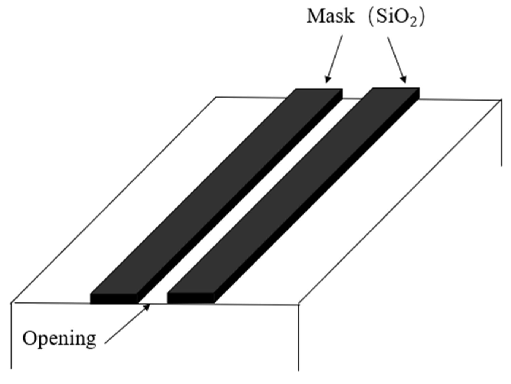
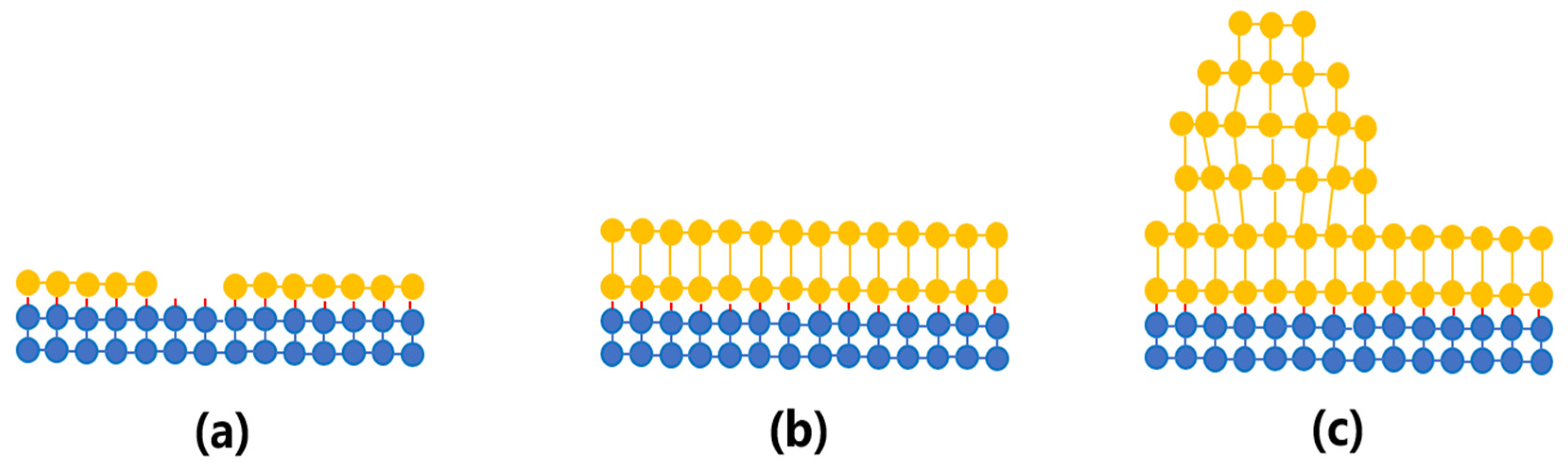
2. Principles of SAE

SAE refers to the method of growing materials with different thicknesses and compositions at various locations on the same wafer. It involves the deposition of a dielectric material on the substrate as a mask, most commonly silicon oxide (SiO2). After designing the desired substrate pattern, the substrate was divided into regions covered by the mask and exposed areas using pattern techniques. The most straightforward and practical mask pattern is a pair of rectangular strips, as shown in Figure 1. The area exposed between the two stripes was the mask-opening region. The dielectric mask can inhibit the precursor deposition and nucleation. As a result, deposition and growth occur only in the opening region and hardly on the mask, realizing the selective growth of the material on the substrate.
The mask material should have a low sticking coefficient to the precursor gas [11,12], can withstand high temperatures [13], is insensitive to precursors, and is compatible with subsequent processes, such as inductively coupled plasma (ICP) or chemical wet etching [14]. Common mask materials are amorphous SiNx and SiO2.
Pattern techniques realize the design of a patterned mask over the substrate. There are three primary patterning design methods. Deep ultraviolet (DUV) lithography realizes the mask size in the hundreds of nanometers [15]. Electron beam lithography (EBL) can enable the resolution of SAE on a scale of tens to hundreds of nanometers [16]. Nano-imprinting lithography (NIL) can realize the pattern design of wafer-level size.
The geometry and size of the mask affect the epilayer thickness and composition obtained via SAE compared to the uniform epilayer obtained by MOCVD on exposed planar substrates. The successful fabrication of lasers and integrated optoelectronic devices is based on the control of the surface morphology and the composition of selective area growth.

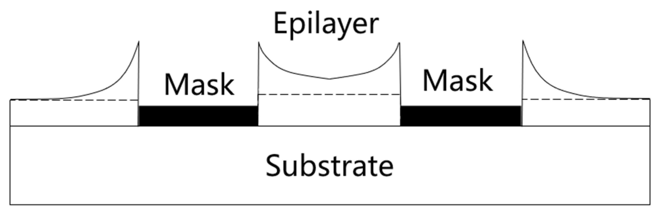
2.1. Growth-Rate Enhancement and Composition Variation

The growth-rate enhancement (or “growth-enhancement effect”, GRE/GEE) effect is one of the essential properties of SAE. During the MOCVD process, the precursor gas-phase molecules were selectively adsorbed at the substrate opening, whereas few molecules were attached to the mask surface. This occurred because the sticking coefficients of precursors on the mask were much lower than that of the surface of the epitaxial region in the high temperature of MOCVD. The mask suppressed the nucleation of the crystals. Material growth occurred selectively in the opening region. According to the conservation of mass, the concentration of the precursor above the mask was larger than that of the opening area. The precursor gas was transported from the mask to the opening driven by the concentration gradient. The material grown on the opening area of the masked substrate was thicker than that grown on the unmasked planar substrate at the same time. The deposition rate near the edge of the stripe mask was higher than that of the opening area far from the mask. The lateral gas diffusion over the mask area to the opening area leads to this phenomenon [17,18,19]. The phenomenon mentioned above is the GRE. GRE is expressed as the ratio of the thickness of the film grown at the opening area on the masked substrate to the thickness of the film grown on the unmasked wafer. Figure 2 shows a schematic of the cross-section of the GRE cross-section.
Another critical property of SAE is the compositional variation with the GRE. The MOCVD growth of III–V alloys on wafers is dominated by the absorption and vapor-phase diffusion of III species. The absorption, surface migration, and re-evaporation capabilities of III-group molecules on the mask are different. These processes affect the flux of III-species gas absorbed on the mask reaching the opening area.
A compositional variation appears in the opening area, especially in the sidewalls of the growth layers near the edges of the strip masks, as diffusion from the mask to the unmasked wafer occurred [20,21].
The typical opening width between the mask was 5–20 μm, and the stripe width was 5–50 μm; the material growth in the openings was determined by the widths of both the oxide mask and the opening [22]. The thickness and GRE of the growth layer increased as the width of the mask increased, which was the exact opposite of the case noted considering the opening area [23]. The GRE was still clearly visible in the opening area with a 100 μm width [24]. The GRE disappeared at positions very far from the edge of the mask stripes, which does not differ from the case involving growth on a planar substrate. The controllable growth of layers with different thicknesses and compositions was realized by changing the spacing and width of the mask stripes.

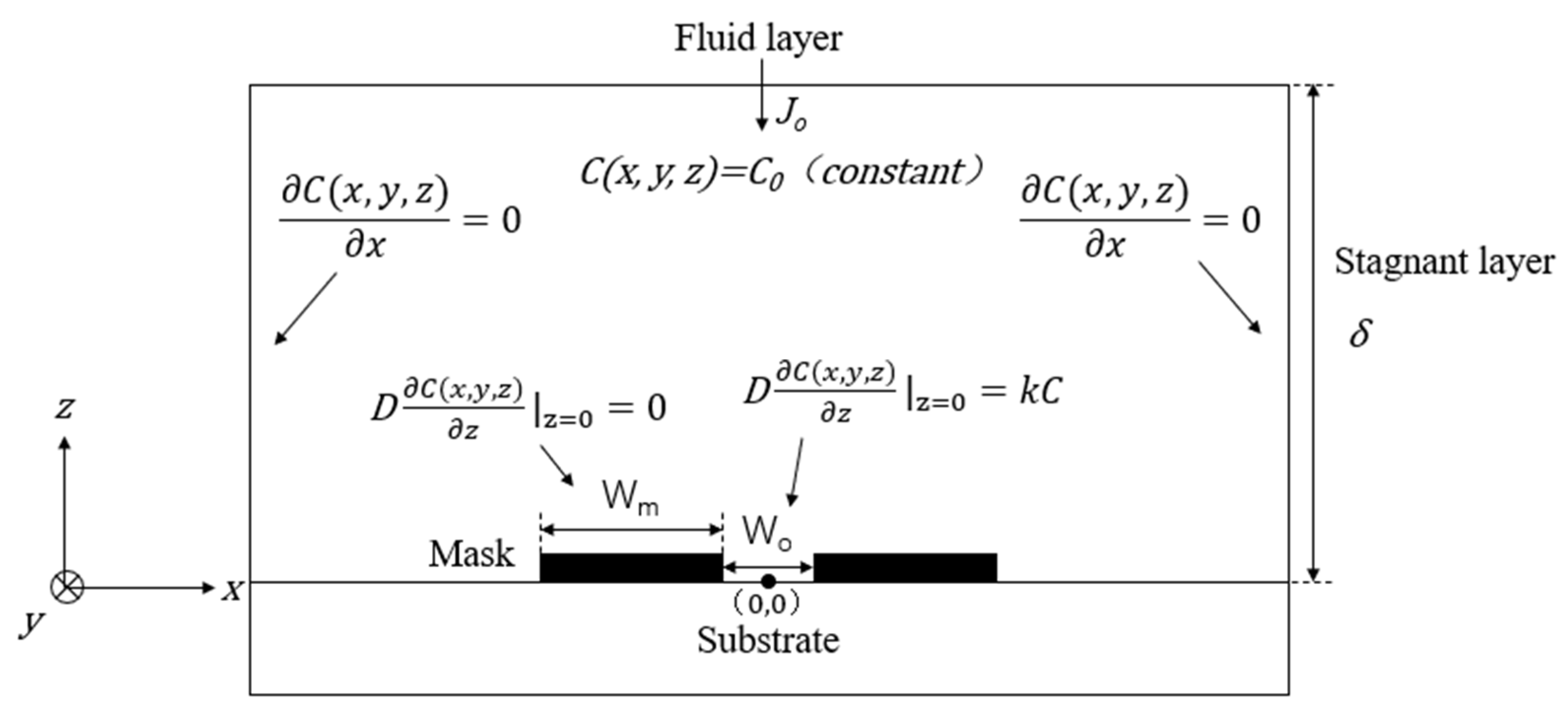
2.2. Vapor-Phase Diffusion Model of SAE

Several studies have proposed models for SAE-grown materials that quantify the diffusion process. The GRE and composition shift were considered functions of the mask geometry. The GRE mechanism comprises two parts: surface migration and vapor-phase diffusion [23]. Surface migration was thought to occur because the gas molecules absorbed on the dielectric mask migrated along the surface of the mask and the sidewalls of the epilayer. Vapor-phase diffusion refers to the flux to the unmasked region due to the concentration gradient of the undeposited precursor above the mask. The mask width is typically on the order of tens of micrometers. Surface migration in the masked area is ignored as it only occurs within a few microns of the mask surface [25].
The three-dimensional vapor-phase diffusion model is established by solving the state diffusion equation in an assumed region that is similar to the experimental conditions, as shown in Figure 3. The thickness and composition profiles of various compounds were predicted using vapor-phase diffusion calculations.
The model assumed a stagnant area above the wafer. The height of the stagnant area is “δ”(~500 μm) [22]. The fluid layer above the stagnant layer provided a constant flow. In the equations below, D and k are the diffusion length and reaction rate of the reactant precursor, respectively. Wo and Wm are the widths of the opening area and masks, respectively. C is the concentration of the reactant gas molecules, usually group-III species. The growth direction was z, and the length along the mask was y. The horizontal direction, x, is perpendicular to the z- and y-axes.
Because the spatial gas concentration is constant, the substance diffusion equation in three-dimensional space is
2 C x 2 + 2 C y 2 + 2 C z 2 = 0 .
Above the stagnant area, the concentration of precursors is constant.
C ( x ,   y ,   z = δ ) = C 0
The symmetry of the computational domain defines the left and right boundaries is expressed as
D C ( x , y , z ) x = 0 .
There is no growth occurring on the mask surfaces.
D C ( x , y , z ) z | z = 0 = 0
The growth process in the unmasked region is given by
D C ( x , y , z ) z | z = 0 = k C .
In this model, D/k is the effective diffusion length of the species. The relationship between the effective diffusion length and mask length determines the dominant process in GRE. Surface migration plays a major role when the mask geometry is close to the surface-diffusion length. On the contrary, the vapor-phase diffusion model dominates this process because the mask size is larger than the diffusion length [26]. A decrease in the effective diffusion length increased the growth rate next to the stripe mask. The vapor-phase diffusion equations for different III-species precursors were obtained to obtain the GRE and composition changes.
The GRE factor R is expressed as
R = C ( x , y , z = 0 ) C ( 0 ) ,
where C(x, y, z = 0) is the concentration of group-III vapor-phase molecules on the z = 0 plane, and C(0) is the analytic solution of Laplace’s equation for the unmasked wafer. C(0) is expressed as [27]
C ( 0 ) = C 0 k D δ + 1
Model calculations were performed without considering the interactions between the different III species [28]. Dupuis et al. [25,29] assumed that the growth-rate enhancement of ternary or quaternary alloys was linearly related to group-III precursors. They gave the expressions for the growth-rate enhancement factor of AlxGayIn1−xyAs system film and III–element composition.
R ( A l x 0 G a y 0 I n 1 x 0 y 0 A s ) = x 0 · R A l + y 0 · R G a + ( 1 x 0 y 0 ) · R I n
A l % = x 0 · R A l R ( A l x 0 G a y 0 I n 1 x 0 y 0 A s )
G a % = y 0 · R G a R ( A l x 0 G a y 0 I n 1 x 0 y 0 A s )
I n % = ( 1 x 0 y 0 ) · R I n R ( A l x 0 G a y 0 I n 1 x 0 y 0 A s )
The reactivity of V precursors is very low at the typical deposition temperatures of MOCVD. The V precursors account for the majority of the gas-phase components, far exceeding the stoichiometric number in the film compound composition, such that it is therefore difficult to obtain an expression of the V composition of the semiconductor compound. Therefore, the deposition rate of III–V compounds is usually determined by the incorporation of III precursors. The GRE becomes more pronounced with the increase of the III–V ratio. At higher temperatures, the desorption of gas molecules on the surface is enhanced, resulting in weaker selective growth. Building an accurate growth-rate-enhancement computational model for these equations helps predict and control the specific growth, including thickness and composition, enabling the design of strain and bandgap energy variations at different locations on a single wafer. The accuracy and efficiency of a diffusion model are vital for the applications of future SAE-integrated optical devices.

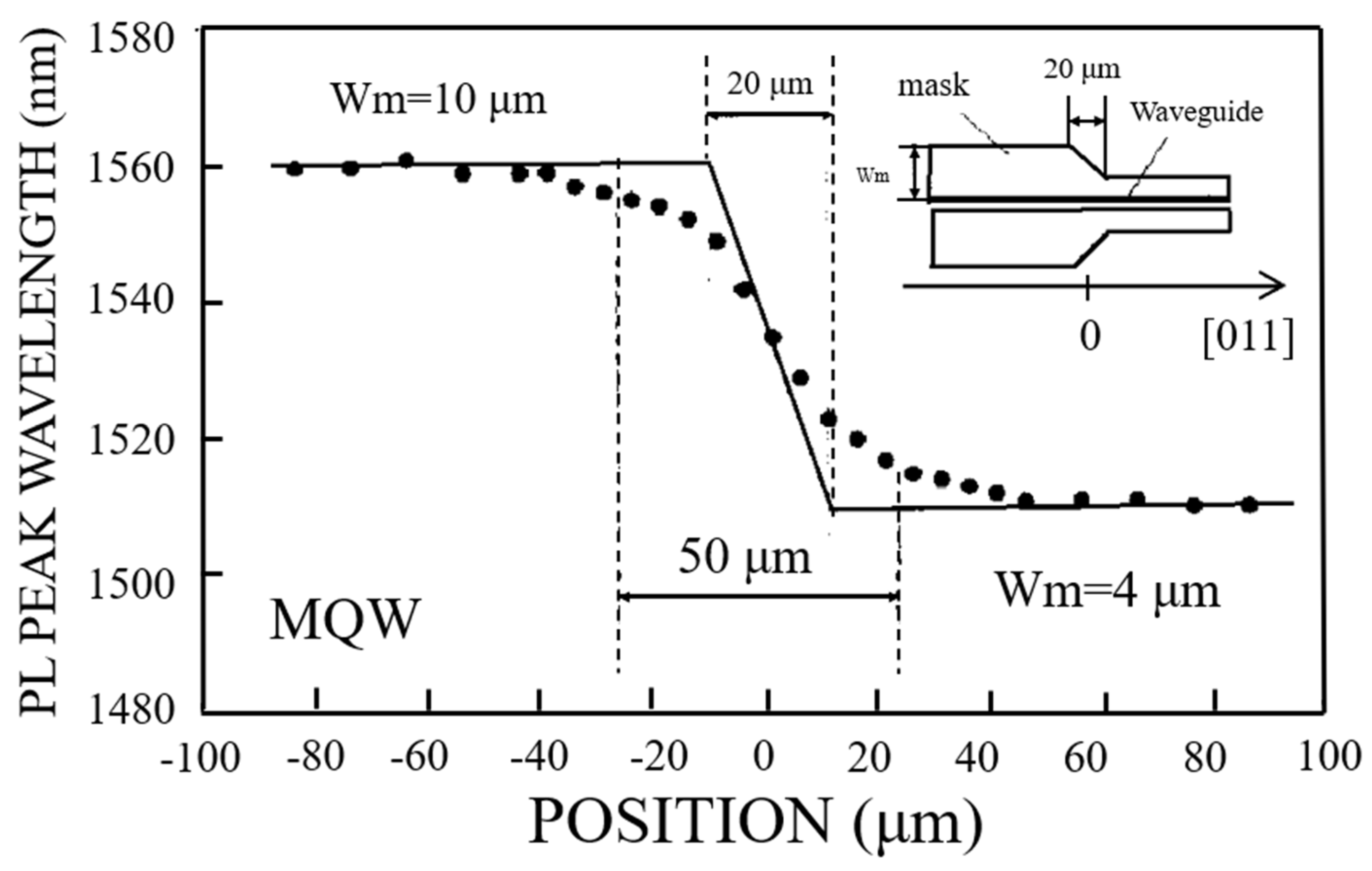
2.3. Bandgap Engineering of SAE

The spatial variation of the energy band and strain for a given patterned mask can be deduced by varying the width of the mask and the opening area. For bulk materials, changes in composition cause a wavelength shift. In quantum wells (QWs), the GRE causes an additional wavelength shift in addition to the composition. The magnitude of the wavelength shifts depends on the width of the mask and the opening area [30]. The effective energy gap, Eg, is sensitive to the thickness of the QW and increases as the layer thickness decreases. The dependence of Eg on the layer thickness enables the tuning of emission wavelength.
Sasaki et al. [31] fabricated a 2 μm wide InGaAs/InGaAsP multiple quantum well (MQW) ridge structure, which was surrounded by stripe masks with various widths on both sides. They observed a 50 nm PL peak wavelength shift by varying the mask width from 4 μm to 10 μm, as shown in Figure 4. A series of studies have demonstrated the relationship between QW emission wavelength tuning and mask geometry [8,28,29].
The gradual gradient wavelength profiles were due to GRE along the edge of the mask. Due to the GRE, there is a thick bulge region at the interface between the mask and the epitaxial layer (Figure 2). Flat interfaces are essential in photonic devices. Adjusting MOCVD parameters, such as increasing the growth temperature [32] and reactor pressure [33], can eliminate convexity near the edge of the mask. The in situ etching process can improve the planarity between the opening area and the masked region [34,35].
Nonplanar growth on a substrate is also an indispensable research topic for SAE. In specific applications, such as butt-coupled waveguides and buried heterojunction lasers, wafers are etched to create grooves with well-defined inclined facets. The orientation of the inclined plane of the groove was different from that of the planar wafer. Distinction of the growth rate in different crystal orientations leads to enhanced diffusion on a nonplanar surface. Different growth rates on different crystal planes also enable the fabrication of high-performance laser structures, such as BH, which will be further discussed in the following sections.

3. Applications of SAE in Semiconductor Lasers

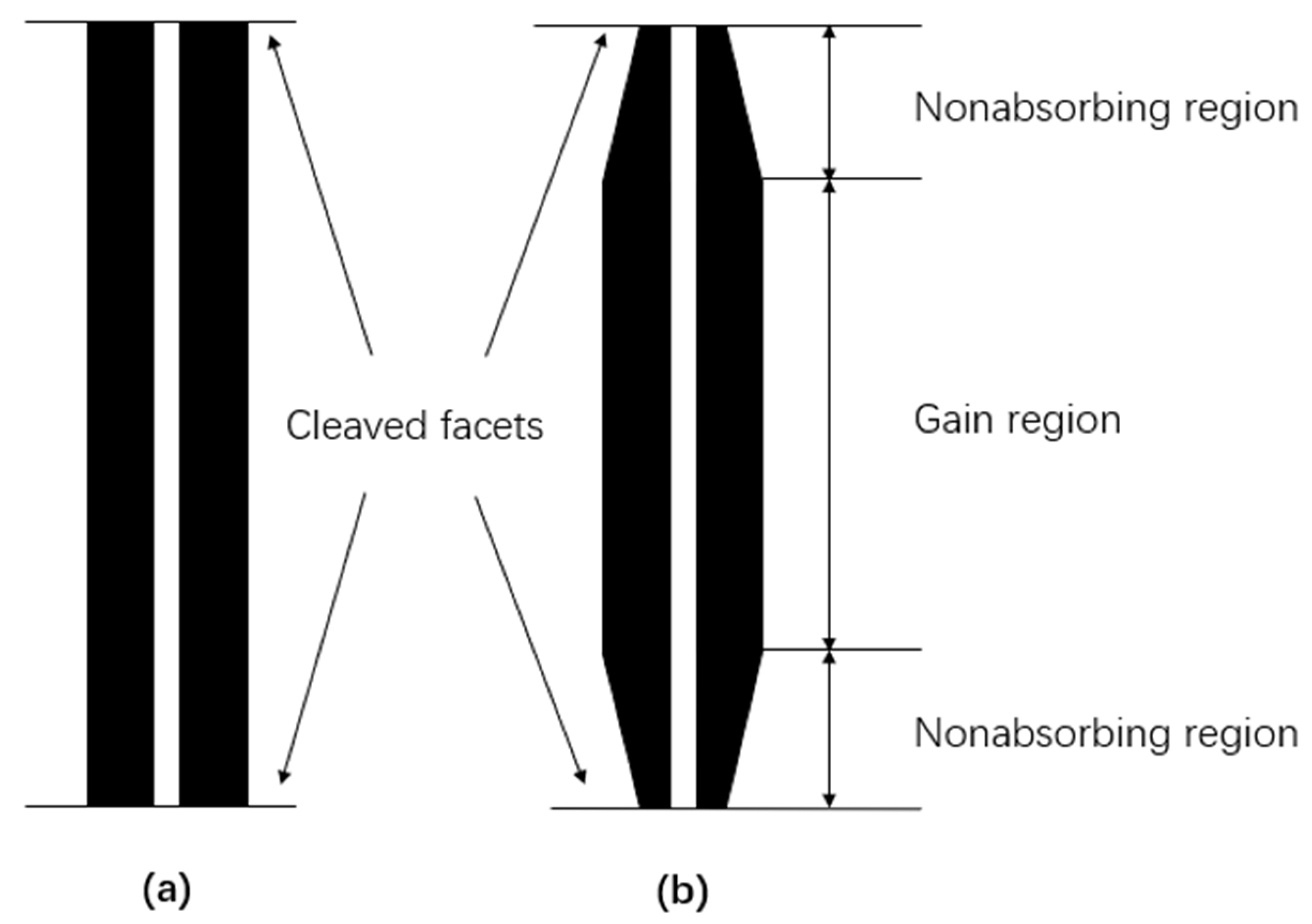
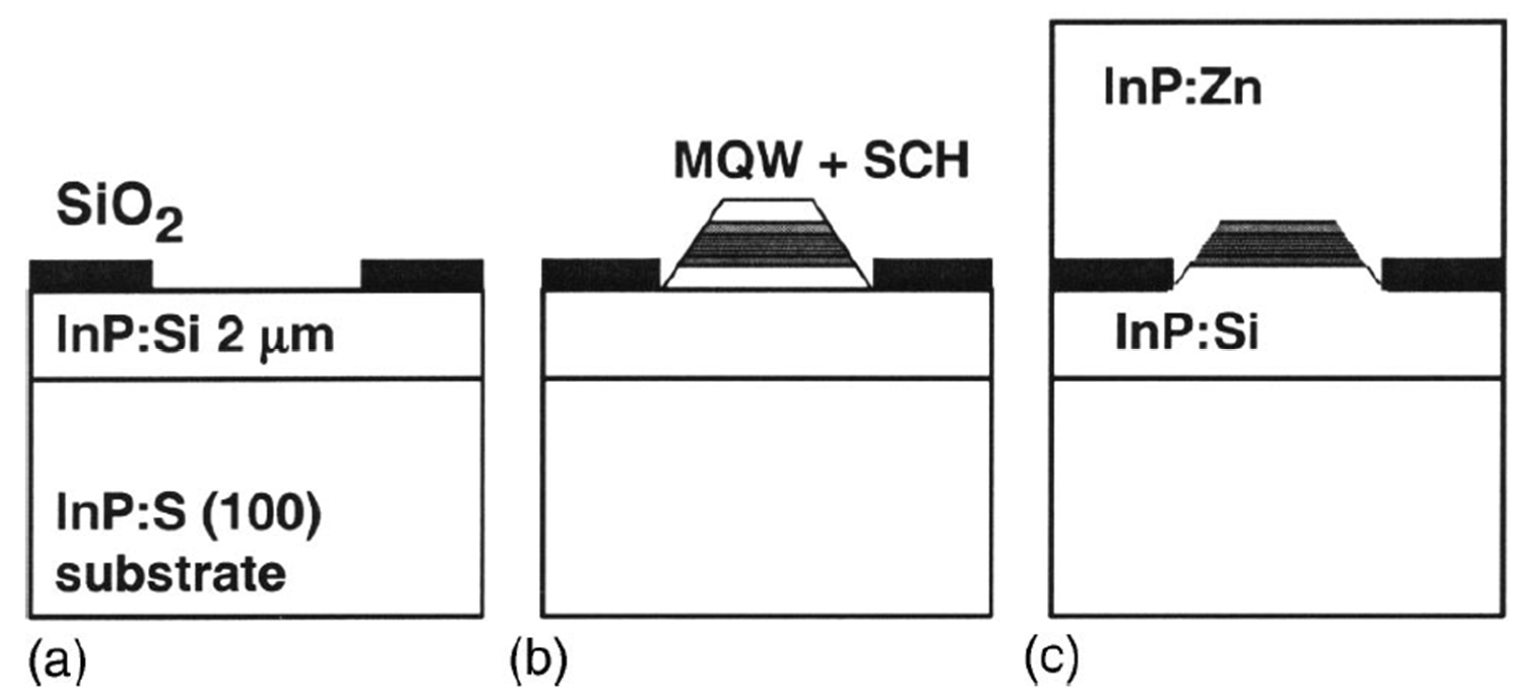
3.1. Buried Heterostructure (BH) Lasers

The active region in a buried heterostructure (BH) laser is completely buried in a wide-bandgap hetero-material. The BH structure has a strong lateral refractive index confinement and current confinement due to the lateral heterostructure [36]. The BH laser has a low threshold current, stable waveguide mode, and nearly symmetrical beam distribution, making it a perfect structure for semiconductor lasers operating with a low threshold and high efficiency. However, conventional BH lasers require multiple MOCVD steps, easily introducing contamination and oxidation to the surface. The SAE can complete the BH structure in a single growth step, eliminating the related defects.
Galeuchet et al. [37] presented a GaInAs/InP heterostructure grown in one SAE step. The GaInAs active layer growth occurred on the (100) facet rather than {111}, where the InP layer growth took place. Different sticking coefficients or diffusion constants of InP and GaInAs may be responsible for the different growth in the (100) and {111} facets. The nucleation sites of the {111} A facets were occupied with stable molecules that did not react to a large extent, while the {111}B facets were active and provided reactants to the (100) facets. The width of the mesa decreased as the growth proceeded. Finally, the lateral size of the buried layers became zero, and the sides of the sloping {111}B facets merged into one. A BH laser was fabricated in one growth step because the GaInAs layers were buried in the InP. The catastrophic optical damage (COD) due to the absorption in the active region near the output facets usually occurs in high-power semiconductor lasers. This limits the high-power output of lasers. Lammert et al. [38] presented a BH laser with a nonabsorbing mirror region, where a fusiform patterned mask was used, as shown in Figure 5. The output power of the BH laser with nonabsorbing mirrors exhibited increments of 40%.
Epitaxial structures with different thicknesses and compositions were obtained by designing the mask geometry. Semiconductor lasers are integrated with other waveguides on the same wafer to form optoelectronic devices for various purposes. Kobayashi et al. [39] proposed an MQW BH laser integrated with a reduced-thickness waveguide layer. Both the gain and waveguide regions were simultaneously grown by SAE on a (100) InP-patterned substrate. The far-field FWHM of the device was 11.8° vertically and 8° laterally. The threshold current was 19 mA, with a high slope efficiency of 0.25 mW/mA. Takemase et al. [40] reported an AlGaInAs BH laser with a mode profile converter (MPC) for the first time. The device consisted of a constant thickness portion as the gain region and a vertically tapered thickness portion to expand the beam output. The gain region and thickness-tapered portion were grown via SAE. The width of the opening area between the two masks was 20 μm. AlGaInAs MQW was grown between the mask stripes with a width of 100 μm. The gain layer was approximately two times thicker than that of the end of the tapered region. The SiO2 mask was removed using HF after the current blocking layers were established. The characteristic temperature was 43 K at 60 °C. The poor temperature characteristic was attributed to the poor crystal quality of the AlGaInAs grown by SAE.
Bour et al. [41] described a self-aligned BH AlGaInAs QW laser using a micro-SAE. The general process of fabricating a self-aligned BH laser with a single growth step is shown in Figure 6. The 50 nm SiO2 mask stripes were formed along [011] on a 2 μm InP n-cladding layer. The widths of opening region and masks were 1.5 and 7 μm, respectively. The sample was returned to the MOCVD reactor for growing AlGaInAs MQW and a separate confinement heterostructure (SCH) under high temperature conditions, accompanied by the {111} B sidewall formation, as shown in Figure 6b. The InP layer nucleated on the {111} sidewall when the temperature was lowered, because of a decrease in the surface mobility, and therefore the InP p-cladding layer was developed and encapsulated in the active region (Figure 6c). The SiO2 mask was used as the current blocking layer without removal in the finished device, whose performance was improved compared to the conventional reverse-biased p–n junction.
Cai et al. [42] obtained an InGaAs/InGaAsP MQW BH laser in a single growth step. InP cladding layer was grown on {111} B sidewalls. The threshold current of the BH laser is 2.7 mA at room temperature. After a burn-in test of 600 h, the total degradation of the outpower was less than 6%, and the BH laser had excellent reliability. The SAE method has great potential for low-cost high-performance BH laser fabrications and associated device integrations due to its excellent performance and inherent manufacturing simplicity.

3.2. Quantum Dots (QD) Lasers

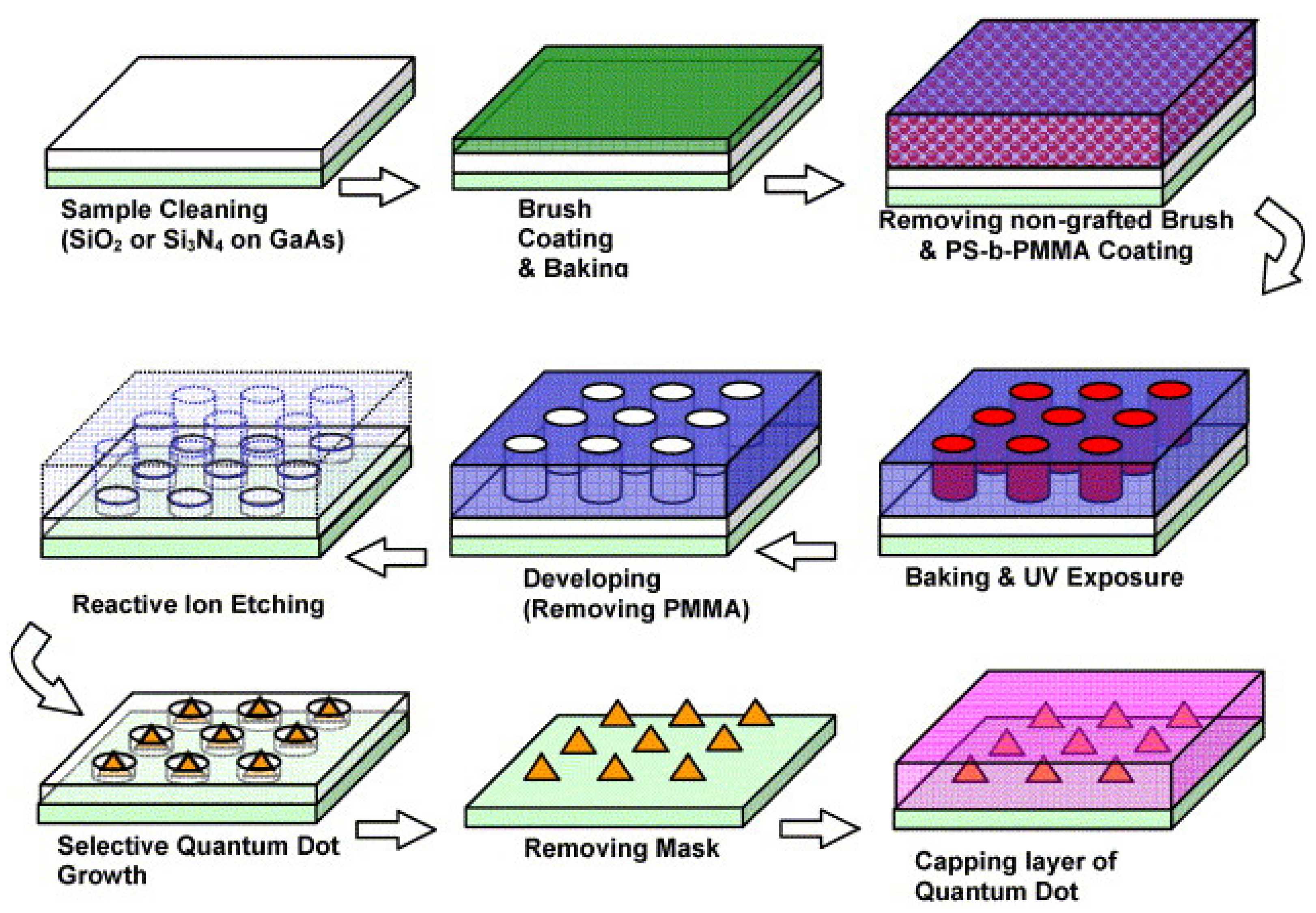
3.2.1. QDs Lasers by EBL and Lithography

Semiconductor quantum dots (QDs) that achieve full three-dimensional confinement are sphere-like nanostructures with strong carrier confinement effects. However, in MOCVD and MBE, pyramidal or cylindrical QDs are obtained due to the existence of a wetting layer. They are typically embedded in another material with a large bandgap. Since QDs have a lower threshold current density, narrower gain spectrum, higher optical gain, higher temperature stability, and better dynamic characteristics than QWs, they are an ideal gain medium for semiconductor lasers. However, it is challenging to grow QDs with uniform size and controlled position. The growth of high-quality QDs is a popular research topic.
The typical QD growth mode is Stranski–Krastanov (SK) growth, relying on strain-driven self-assembly between different material layers. If the strain is too high to grow continuous layers, the later-grown layers split into nanoscale islands when they reach a thickness of several single atoms. Subsequently, the island structures were embedded in an extensive–bandgap material to form QDs. This process is known as SK growth (Figure 7). The QD obtained using this method is called self-assembled QDs (SAQDs). The precisely controlled diameter and thickness of the QDs can stabilize the energy-level distribution without broadening the laser gain spectrum. The gain increased as density of the QDs increased. The operating threshold and gain spectrum characteristics of QD lasers were better than those of QW lasers. However, SAQDs have two disadvantages: (1) the presence of a wetting layer causes incomplete three-dimensional confinement and (2) the randomness of the nucleation position and the variation in size (diameter, thickness) also limit the advantages of QDs. Both lead to a shift in the quantized energy level and the non-uniform broadening of the gain spectrum, which is broader than that of QWs.
The SAE is a method used to overcome the shortcomings of SAQDs’ growth. The patterned grown QDs have no wetting layers and can control their position and diameter to obtain uniform QDs. The most widely used method of fabricating QDs by SAE is to first pattern a mask on the substrate with high-resolution lithography, ensuring that the size of the opening region is small enough to grow QDs.
Elarde et al. [43] combined EBL and SAE to prepare uniformly distributed QDs. The EBL was used to define the exact location of QDs’ nucleation, and the SAE realized the control of QDs’ geometries by patterned SiO2 masks. They deposited 10 nm SiO2 and patterned 4, 6, and 8 μm mask stripes using optical lithography and wet etching on n-type Al0.75Ga0.25As cladding and GaAs barrier layers. Their samples were coated with polymethylmethacrylate to obtain arrays of 30 to 40 nm circular features in diameter using EBL. The arrays were centered over the SiO2 mask stripes. After the array pattern was transferred to the SiO2 masks by wet etching, 6.9 nm-thick In0.35Ga0.65As QD layers were formed and encapsulated by 10 nm GaAs. The p-type cladding and contact layer were then grown during a later stage. The density of the fabricated QDs with a center spacing of 100 nm was 1.2 × 1010 cm−2, and the diameter of QDs was an average of 80 nm. This report combined EBL and SAE to manufacture the first QD laser.
Mokkapati et al. [44] presented the InGaAs QD laser with different lasing wavelengths. When the width of the stripe was as small as 5 μm, QD intensity could provide insufficient gain for lasing. Correspondingly, an excessive thickness of InGaAs was obtained when the stripe width reached 20 μm, introducing defects and increasing losses. Akaishi et al. [45] fabricate a series of SiO2 stripe masks uniformly arrayed on the InP substrate. They utilized a SiO2 mask array consisting of a wide mask on the side and a series of relatively narrow mask stripes. By changing the width of the wide mask while maintaining the narrow stripe masks at 3 μm widths, the sizes of the InAs QDs varied in each opening region. The double-capped layer enabled the uniform height of QDs. When the width of the wide stripe mask was 200 μm, the emission wavelength range of the QD array grown between the narrow masks exceeded 120 nm.

3.2.2. QDs Lasers by Block Copolymer Lithography

Morever, patterned QDs can also be prepared by block copolymer (BCP) lithography. A typical diblock copolymer consists of alternately polymerizing two polymers, one of which is miscible in small amounts in another polymer. This immiscibility leads to the phase separation of the two materials and maintains the properties of each material. The interaction between the two polymers produces a QD pattern. The absence of a wetting layer resulted in perfect three-dimensional confinement. Figure 8 presents the process of SAE QD fabrication using diblock copolymer lithography.
Polystyrene-block-poly (PS-b-PMMA) was the diblock copolymer in this process. First, the amorphous mask materials were deposited onto the substrate using plasma chemical vapor deposition (PECVD). Then the PS-b-PMMA brush was coated above the mask. After spinning the PS-b-PMMA on wafers, the entire structure was exposed to UV such that the PS area was exposed as the pattern template upon the removal of PMMA. ICP transferred the pattern into the mask layer, followed by the removal of the PS region via etching. Finally, the selective area growth of QD was accomplished in the cylinder hole.
The uniform size distribution and spatial position of QDs fabricated by block copolymer lithography provide more significant advantages than SAQDs grown in SK mode. Li et al. [47] obtained uniform GaAs QDs with a density of approximately 1011 cm−2 by selective growth in the narrow openings of SiNx patterned masks using block copolymer lithography. Kim et al. [48] fabricated GaAs/InGaAs/GaAs compressive–strain QDs using SiNx patterns defined by block copolymer lithography. Figure 9 shows the InGaAs QD laser structure. The CBr4 in situ etching time was optimized to reduce the processing damage before growing the QDs, leading to a decrease of the nonradiative recombination centers of the QDs. Compared with the devices grown using non-optimized in situ etching times, the QD lasers grown using optimal etching times significantly reduced the threshold and transparency current. Furthermore, Kim et al. [49] fabricated an InAs QDs laser with an In0.1Ga0.9As QW carrier collection layer to increase the carrier injection into the QDs. The QD laser achieved lasing at RT.

3.3. Heteroepitaxy Lasers on Si or SOI

The natural characteristics of indirect bandgaps limit the wide applications of silicon photonic devices. This inherent property results in weak light emission and poor optoelectronic performance. Direct bandgap materials exhibit good luminescence properties. The direct bandgap III–V semiconductor lasers are high-performance light sources that may be utilized for silicon photonic integrated circuits. However, a high density of threading dislocations (TDs), planar defects, and anti-phase boundaries (APB) arises at the interface of III–V and silicon [50,51,52,53], owing to the mismatch of lattice constants, thermal expansion coefficient, and polarity between III–V materials and silicon. There is great research interest in finding methods for growing lattice constant-matched or low-defect-density III–V light sources directly on silicon. Defects introduced by the lattice and polarity mismatches between the III–V materials and Si have been substantially eliminated in a previous study using a template in conjunction with bonding techniques [54]. However, it is expensive and time-consuming to prepare such templates. Therefore, it is more desirable to directly epitaxially grow high-quality III–V materials on Si.

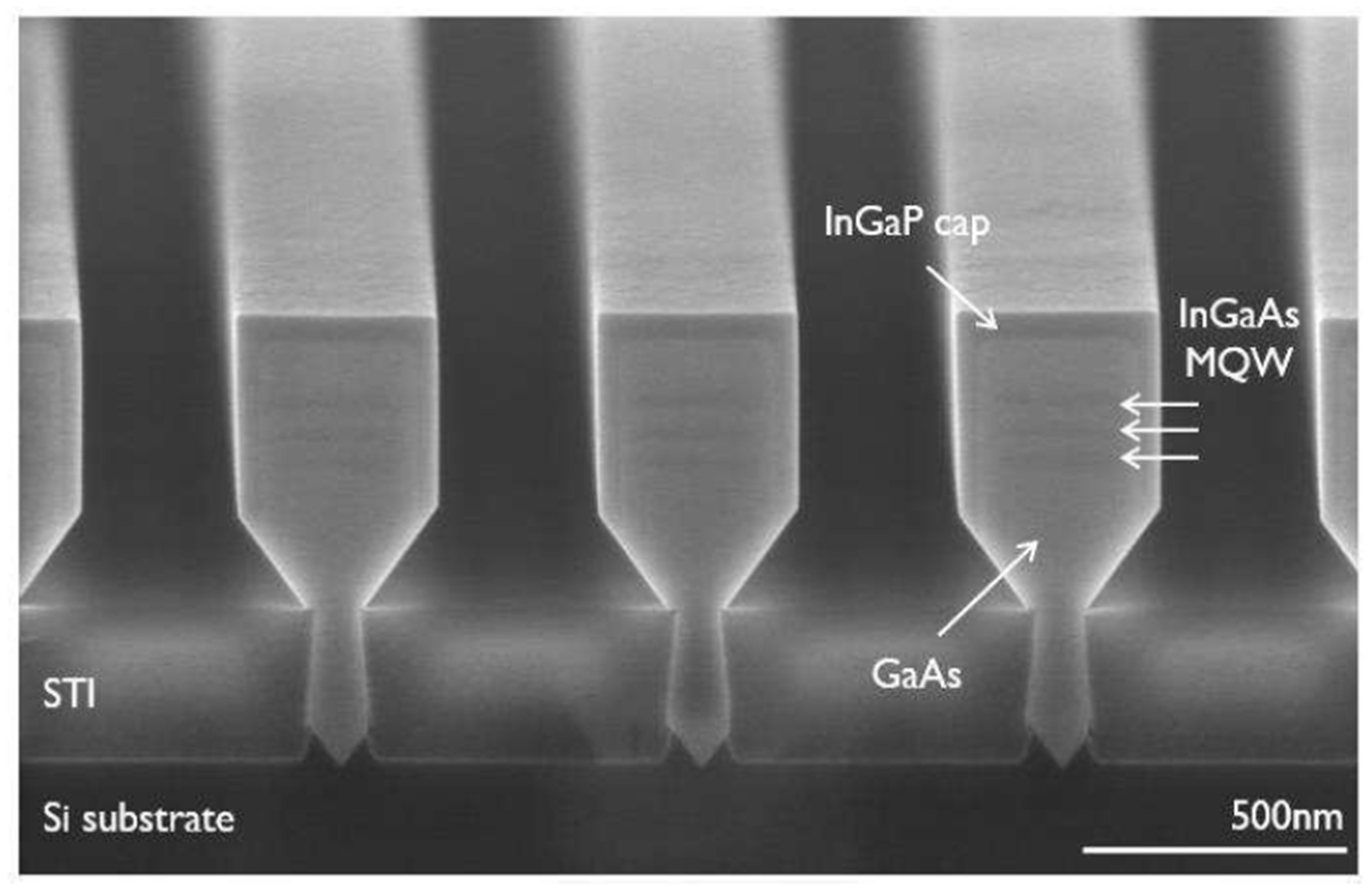
3.3.1. Aspect Ratio Trapping (ART)

Bonding technology is the most common III–V/Si integration technique, combining a known good III–V epitaxial layer with a silicon platform. The main shortcomings of the bonding technique are the strict requirements for ultra-clean and highly flat surfaces, the high thermal resistance introduced by the oxide during bonding, and the wafer size mismatched between the Si substrate and the III–V (InP and GaAs) material substrate. These shortcomings limit the high-density integration of laser on silicon [55]. The local bonding process is technically challenging and expensive, not conducive to mass production [22]. SAE has become an economical and reproductive approach for relieving the defects resulting from mismatched crystal growth and realizing the local integration of III–V lasers on a silicon platform. Figure 10 presents the principle of SAE to decrease dislocation densities in the epitaxial layer at the interface of III–V materials and silicon.
The growth begins in narrow openings on the masked substrate. The dislocations that occur at the interface of III–V and silicon because of the heavily lattice-mismatched can only propagate along a certain angle inclined to the substrate plane from the opening area to the epitaxial layer. For Si (0 0 1) substrates, the dislocations propagate along with the <1 1 1> directions, forming a 54.7° angle with (0 0 1). The thickness of the materials exceeded that of the mask as the growth process proceeded. The epitaxial layer grows laterally along the mask surface, which is referred to as epitaxial lateral overgrowth (ELO or ELOG). Dislocations cannot propagate into the mask and vanish in the epitaxial layers because the interface lattice between the crystalline material and the amorphous mask is discontinuous. If the growth time is sufficiently long, the epitaxial layer grown in the opening region merges with the layer grown in the neighboring opening region to form a complete epitaxial layer above the masks. The mask effectively prevented dislocation propagation, and the dislocation density distributed in the lateral overgrowth partial of the epitaxial layer was several orders of magnitude lower than that grown on the standard unmasked substrate. Figure 11 shows the cross-sectional TEM image of the ELOG InP with SiO2 masks on silicon. The region above the mask was dislocation-free. Figure 11a shows that the dislocations from the buffer layer could penetrate the region above the mask if the openings were wider than the thickness of the mask. Figure 11b shows that the dislocations were filtered even above the openings if the opening width was smaller than or equal to the mask thickness. There were no coalescence defects above the mask, which refers to defects formed at the junction of two laterally grown InP layers from adjacent openings [56]. This approach, called the aspect ratio trap (ART), has been used in various materials grown on Si [57,58,59].
Moreover, III–V materials grown by ART are on the sub-micrometer scale, which is not conducive to micrometer-scale ridge waveguide fabrication. Han et al. [60] proposed a lateral ART scheme to grow a micrometer-scale InP sandwiched by oxides on the silicon-on-insulator (SOI). A schematic of lateral ART is shown in Figure 12. Compared to the conventional ART grown on (001) Si, lateral ART started at the {111} Si surface, which would not form APBs. The dimensions of the III–V ridge width were limited by the trench width in conventional ART. The size of III–V materials grown in lateral ART is controlled by the thickness of the Si layer, realizing precise micrometer- or nanometer-scale control.
The ART method has been widely used in shallow trench isolation (STI) structures, where a thin Ge layer is typically grown in situ and covers the bottom of the trench as a buffer layer. The lattice mismatch between InP and Ge is only half that between InP and Si, leading to the easier nucleation of InP on the Ge surface [61]. By designing the Ge surface profiles and setting an aspect ratio larger than two, TDs were confined at the bottom of the trench, and APB formation was suppressed [62,63]. GaAs [64,65], InP [66], and InGaAs [67] have been grown on (001) Si with low defect density using SAE technology. After obtaining defect-less high-quality epitaxial layers, III–V materials were grown to fabricate lasers. Staudinger et al. [68] fabricated wurtzite InP microdisks using SAE. They deposited 300 nm-thick SiO2 and patterned approximately 50 to 100 nm line openings. The wurtzite InP was nucleated in the trenches and grew vertically along the [111] A-direction. The zipper-points at the center of the line openings induced ELO after the wurtzite InP extended out of the SiO2 mask, and {1−100} or {11−20} wurtzite facets were formed. The micro-photoluminescence of this system demonstrated that the wurtzite InP microdisk enabled optically driven lasing at room temperature with a threshold of 365 μJ cm−2. Wong et al. [69] deposited 200 nm-thick SiO2 onto InP (111) A substrate using PECVD. They patterned 120 nm ring-shaped mask openings using EBL and ICP. A micro-ring InP laser was obtained via SAE using a two-stage growth process. In the first stage, the temperature and V/III were 750 °C and 300, respectively. The opening areas were completely filled with high-quality wurtzite InP, and ELO occurred. The growth temperature was then lowered to 730 °C, and the V/III content was increased to suppress vertical growth and enhance lateral growth. The micro-ring laser was operated at room temperature with a low threshold.

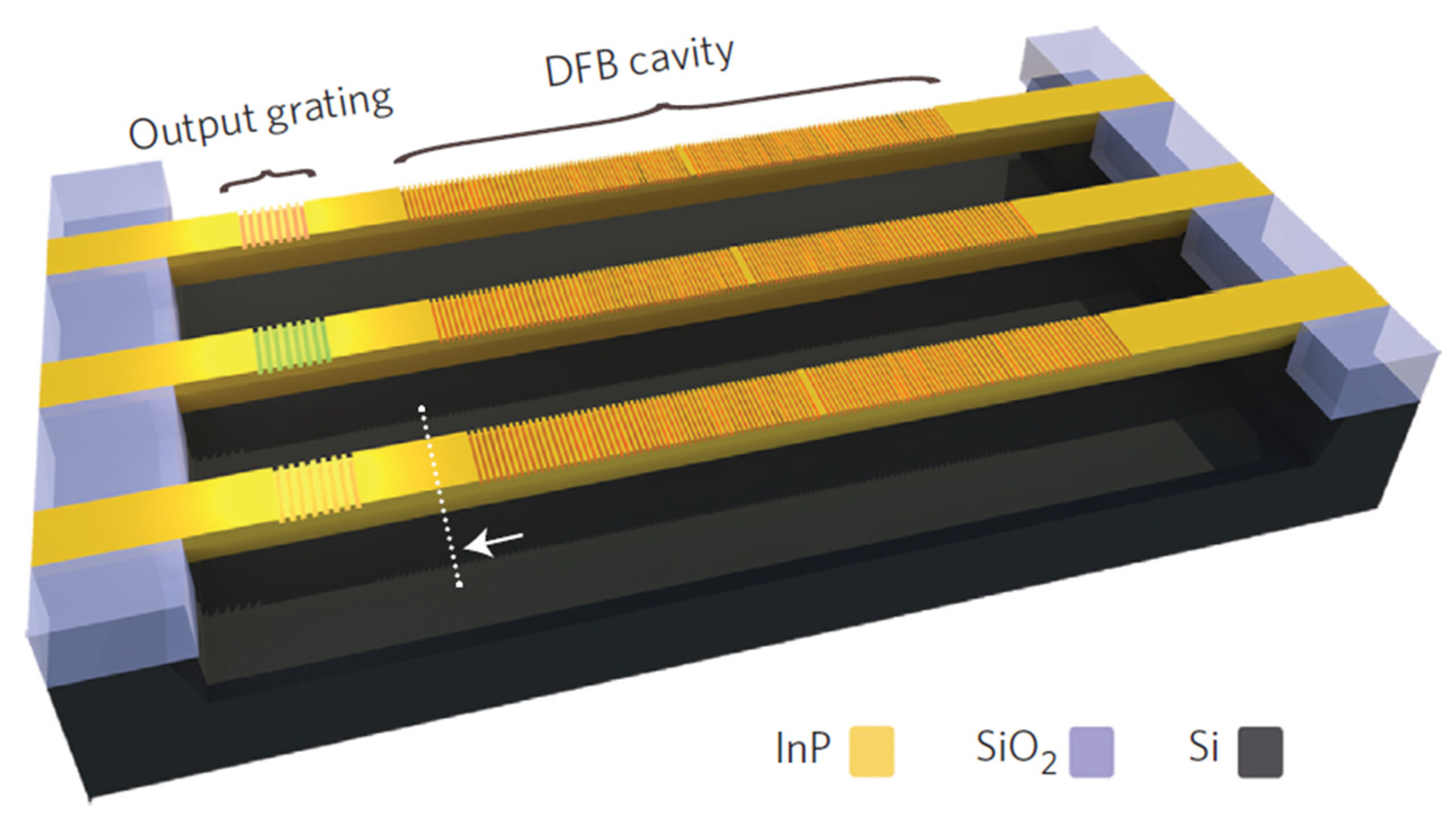
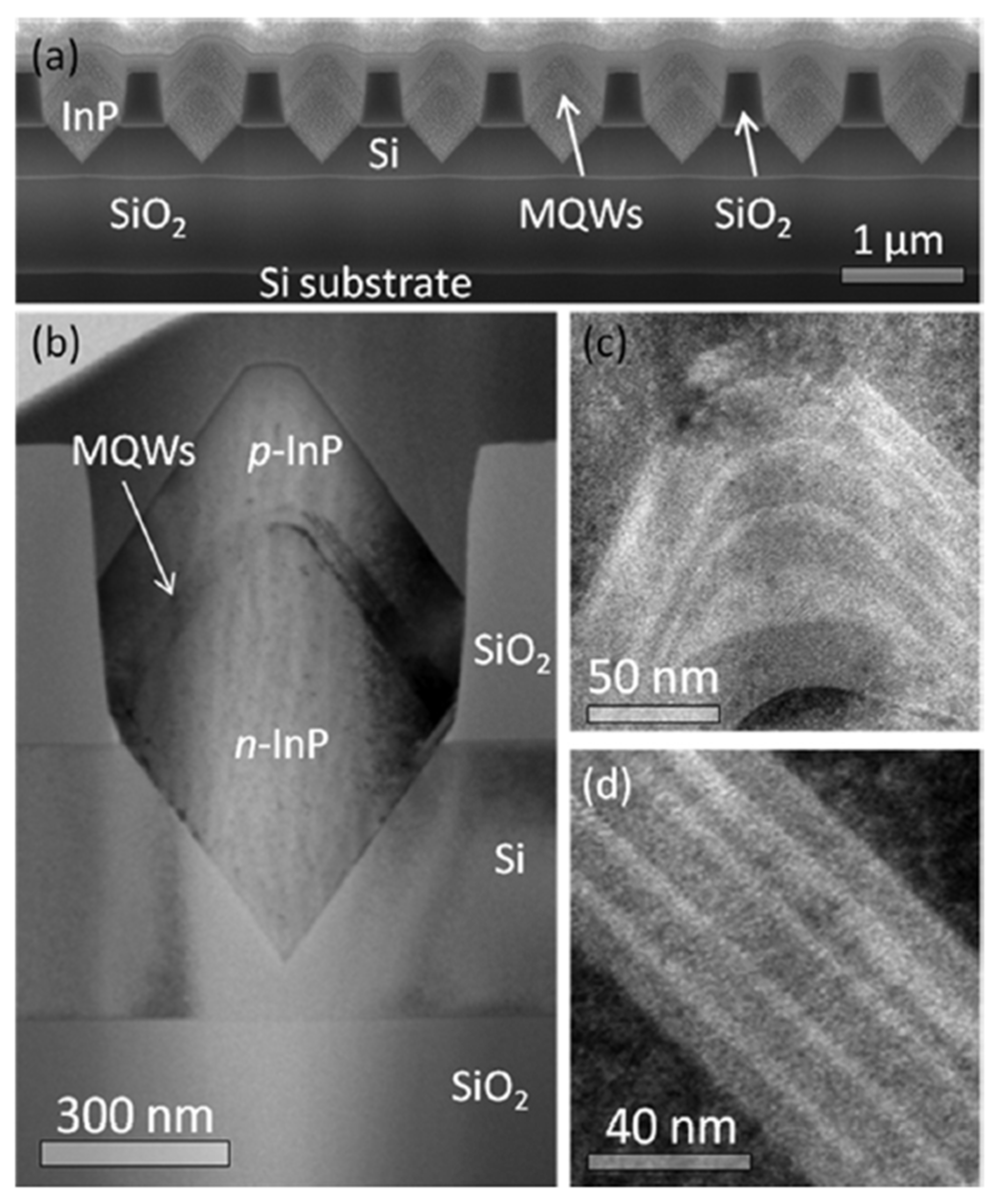
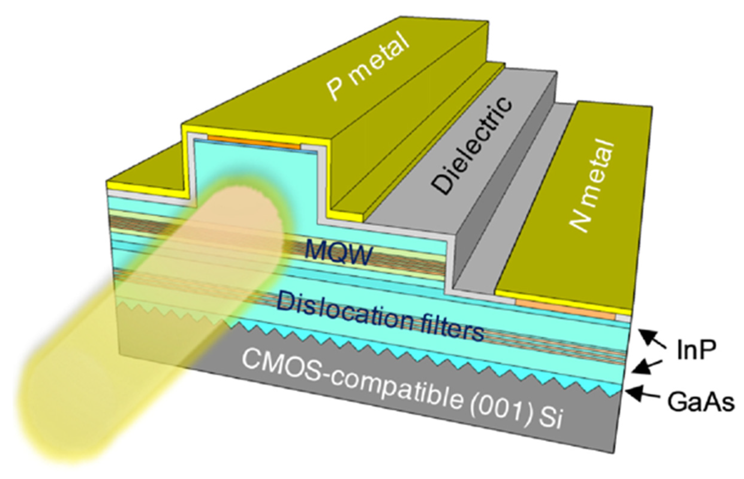
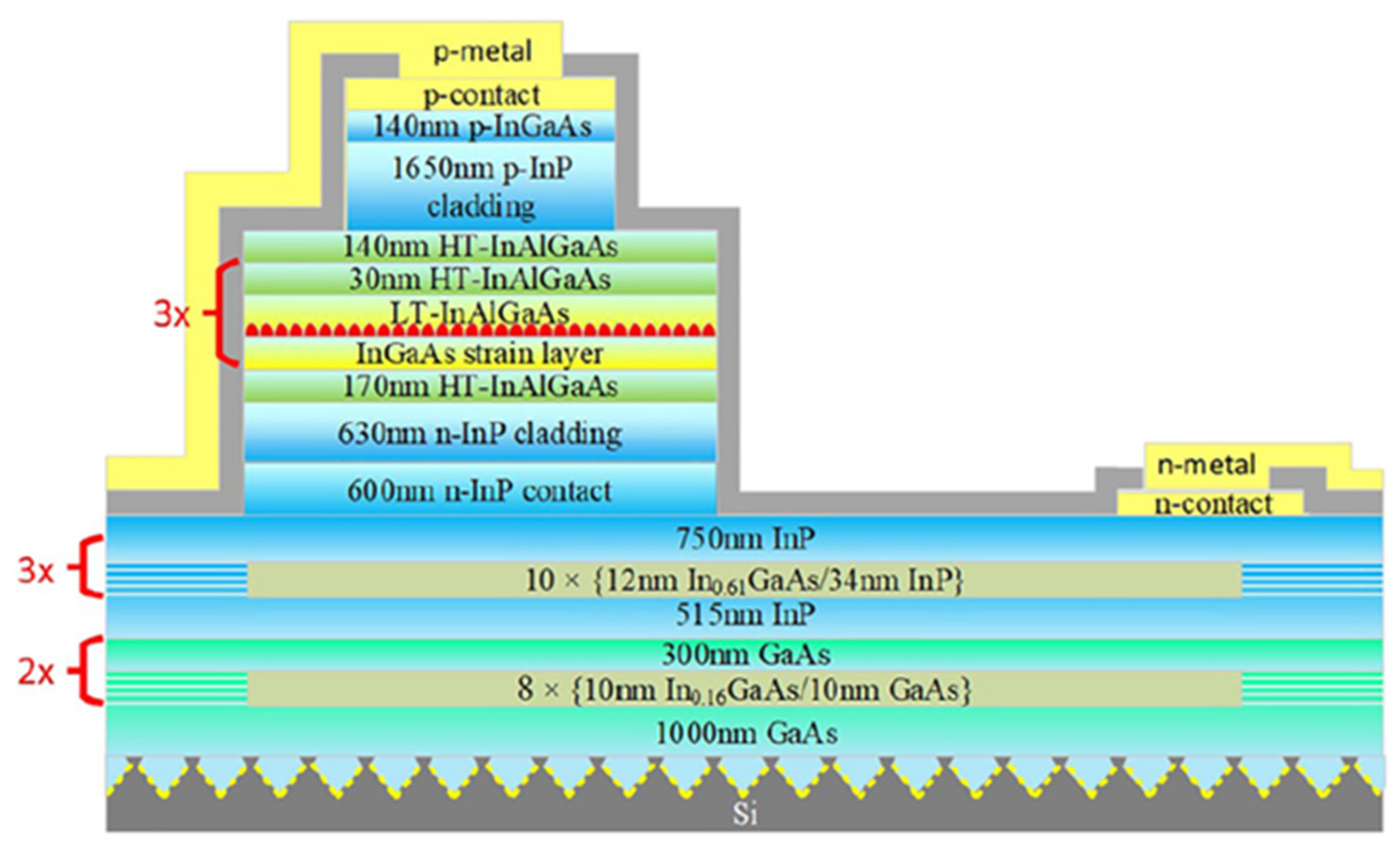
3.3.2. Lasers on Si/SOI

Wang et al. [70] demonstrated an optically pumped InP-based DFB laser array integrated on (001) Si, operating at room temperature using the SAE technique. InP was selectively grown in the trenches of the STI structure. ART limits the defective layer to a thickness of approximately 20 nm, instead of several micrometers. The emitted light can couple with the optical waveguide defined in the same horizontal plane. Figure 13 shows the structure of the device. Each DFB laser in the array contained an InP waveguide with a λ/4-phase shift first-order grating, and a second-order grating was defined 30 μm away from the DFB cavities. The Si substrate below the InP laser was intentionally etched away to avoid pump light absorption. Silicon substrates supported suspended cavities at both ends.
The suspended cavity exhibited thermal, electrical injection, and mechanical stability issues. These problems can be addressed if the laser structure is grown on a SOI. Megalini et al. [71] successfully fabricated InGaAsP MQWs in InP nanowires. SEM and TEM images of the InGaAsP MQWs are shown in Figure 14. The 500 nm-thick SiO2 was deposited on the Si surface and patterned into 200 nm-wide stripes with a spacing of 800 nm. The Si layer was etched by KOH to form V-grooves. The inhomogeneous spectrum shape broadening and wavelength peak emission observed in PL tests were attributed to the poor uniformity of the MQWs, as shown in Figure 14a. The MQWs of {001} were thicker than those of {111}, as shown in Figure 14c,d, which caused a spectrum of inhomogeneous broadening and decreased the lasing material gain. The growth was completed during the V-groove patterning of the SOI to trap most of the defects at the Si/SiO2 interface. The PL peak wavelength of the MQW was 1567 nm.
The mask prevents dislocation propagation and the growth of the ~μm buffer layer using the ART method. Compared to optically pumped lasers, electrically pumped lasers are more challenging to manufacture. There are two main difficulties: acquiring high-quality ternary or quaternary compounds and the fabrication of micrometer-scale ridge waveguides with the constraints of sub-micrometer selective masks. Kunert et al. [72,73] integrated an InGaAs/GaAs heterostructure into box-shaped GaAs ridges with (001) flat surfaces outside the trenches, as shown in Figure 15. An apparent PL of the QW was observed for different ridge sizes. A sufficient III–V volume to fabricate a micrometer-order ridge waveguide can be realized by extending the ridge width.
Several studies have reported on electrically pumped lasers. Shi et al. [74] utilized InGaAs/InP strained layer superlattices (SLSs) as filter layers to suppress the propagating TDs. III–V materials were grown in V-grooved (001) Si to realize ART. They fabricated an electrically pumped InP-based laser at 1550 nm on (001) Si. Figure 16 shows the laser structure. The threshold current density was 2.05 kA/cm2, and the slope efficiency was 0.07 W/A. The maximum output power was 18 mW without facet coating. The continuous-wave (CW) operation temperature reached 65 °C, and the pulsed lasing operation temperature was up to 105 °C.
Wei et al. [75] fabricated a 1.3 μm InAs/InAlGaAs quantum dash (QDash) laser on V-grooved (001) Si. The two sets of eight-period In0.16Ga0.84As/GaAs films were grown above the V-grooved Si as a buffer layer to trap dislocations at the GaAs/Si interface. TDs were filtered in three sets of ten-period In0.61Ga0.39As/InP SLSs. After the n-type InP contact and cladding layers were grown, the three layers of InAs/InAlGaAs QDashes were formed. Finally, the p-type InP cladding and contact layers were deposited. A schematic of the device structure is shown in Figure 17. The threshold current density was 1.05 kA/cm2, and the output power per facet was 22 mW. The laser realized CW operation at 70 °C.
Fujii et al. [76] designed an InP-on-SOI template consisting of an InP buffer layer, InGaAs etch stop layer, and InP layer on a (001) InP substrate. The template was fabricated using a bonding technique. A SiO2 mask was deposited on the template and patterned using photolithography. They successfully fabricated an electrically pumped eight-channel membrane DFB laser array with wavelengths ranging from 1272.3 to 1310.5 nm by adjusting the geometries of masks to optimize the InGaAlAs MQWs on InP-on-SOI. The active regions were buried by n-doped and p-doped InP, which also formed lateral p-i-n structures. A schematic of the membrane laser array is shown in Figure 18. The fiber-coupled output power was greater than 1.5 mW in each channel at 25 °C. The actual lasing wavelength deviated from the designed lasing wavelength by less than 2 nm, and the average channel spacing was 860 GHz.
Several studies on the SAE growth of III–V materials on SOI or Si have been conducted. The aim is to obtain epitaxial structures with a low defect density on Si. The main method is ART, which confines most of the dislocations in a nanometer–thick buffer layer, preventing defects from reaching the surface of the epitaxial layer, thus deteriorating the performance of the optoelectronic device. However, the problem of obtaining high-quality ternary or quaternary III–V compounds limits the epitaxial laser structure on Si.

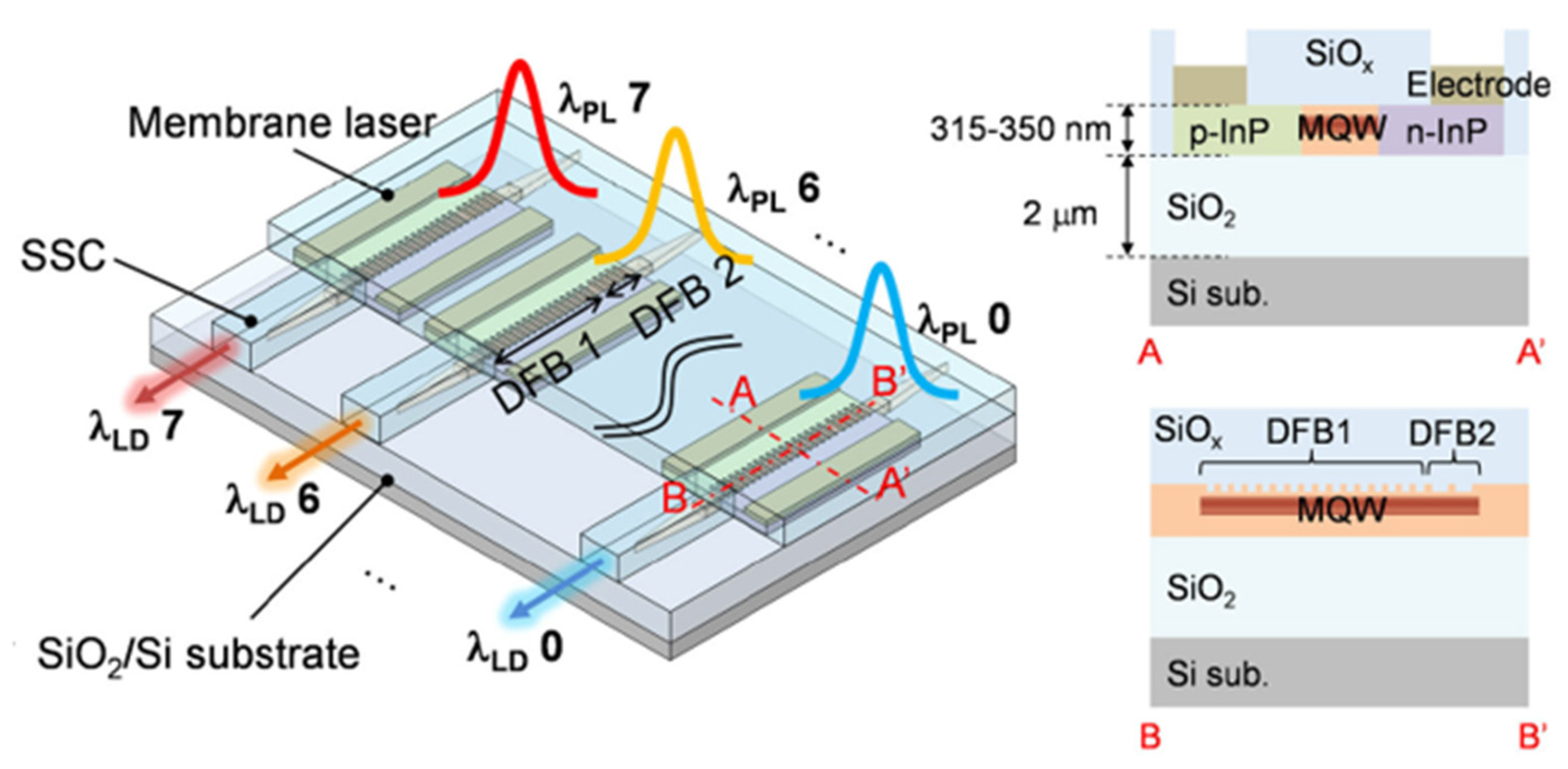
3.4. Integrated Semiconductor Laser
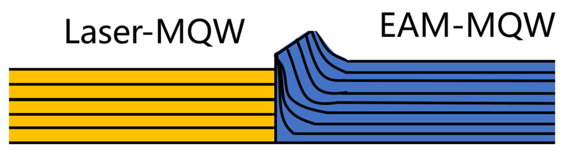
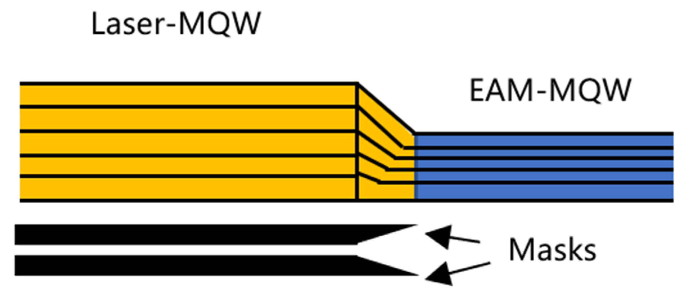
Monolithic PIC has been developed to meet the increasing data flow transmission demand of the Internet. Advanced material growth methods have promoted the development of the PIC. The PIC refers to the integration of numerous optoelectronic components on the same chip [77]. The various device structures in PICs require different energy gaps for each portion of the wafer, and the device must be integrated in a reproducible and cost-effective manner. SAE enables the spatially localized epitaxial growth of the desired material structures for specific chip functions. This is a low-cost and reproducible method to achieve device integration. Recently, integrated semiconductor lasers have included EML and MWLA, which are suitable for wavelength division multiplexing (WDM).

3.4.1. EML

Monolithically integrated EML arrays are a promising light source for modern WDM systems. EML have attracted extensive attention owing to their small size, low packaging cost, low driving voltage, and good stability [78]. In the long waveband of thelong-distance optical communication system, such as 1.31 μm and 1.55 μm, the chirp phenomenon will appear, which is not conducive to the high-speed transmission of information. The modulator is integrated with the laser to form the modulated optical signal source because the modulator can avoid the large-wavelength chirp observed in directly modulated lasers. Using the SAE, the EML is fabricated by combining an electro-absorption modulator (EAM) and a laser on the same chip. Compared with discrete EAM and lasers, EML without fiber coupling reduces loss and cost and improves device reliability. At present, there are two main methods to realize the integration of EAM and laser: butt-joint (BJ) coupling (the laser and EAM are grown separately) and SAE [79].
Figure 19 shows the QWs achieved by BJ, wherein the MQWs of the EAM and the laser are grown in separate epitaxy steps. The MQW laser was grown on the entire wafer in the first step. Then, wet or dry etching was used to selectively etch the region, where the EAM MQW would grow in the second epitaxy. Two epitaxy steps increase the manufacturing cost, and the etched interface became rough and easily formed defects, deteriorating the output performance of the EML. BJ enables the optimization of the laser and EAM.
The SAE technique avoids poor interfaces and multiple epitaxy, as shown in Figure 20. Dielectric oxide masks were deposited and patterned in the laser region. The mask width was changed such that the laser region between the masks had a higher growth rate than that of the EAM region without mask coverage. The lower bandgaps of the MQWs of the laser were formed in one epitaxy step because of the growth-rate enhancement, which avoided the absorption of light due to the rough interface introduced by the etching process between multiple epitaxial growth layers and increased the output power of this system [80]. The disadvantage of the SAE is that the optimal parameters of the active region for the laser and modulator cannot be obtained simultaneously [81]. The bandgap of the MQWs in the EAM region is typically designed to be larger than that of the laser MQWs. The MQWs were grown between and outside of the mask stripes via SAE. The thickness and composition of the MQWs in the two regions differed in one-step epitaxy. The MQWs located between the mask stripes could be well controlled to obtain the desired gain region, while it was difficult to simultaneously obtain perfect EAM MQWs outside of the mask region. For example, the laser preferably exhibited few QWs at the lower threshold current, while the EAM region required more QWs to obtain a high extinction ratio.
Zhao et al. [82] integrated a high-mesa DFB laser and EAM using SAE. The absorption and active regions consisted of an InGaAsP/InGaAsP MQW structure and an optical confinement layer with different thicknesses caused by the fusiform mask, as shown in Figure 5b. The spacing of the two SiO2 mask stripes was fixed at 15 μm, and the mask width varied from 30 to 15 μm in the tapered region. Figure 21 presents a schematic of this device. The EML CW threshold current was 26 mA without the modulation bias for the uncoated laser. The output power of the modulation was 5.5 mW when the current was 100 mA at the laser, in single–mode operation with a side–mode suppression ratio (SMSR) > 40 dB at 1.552 μm. The on/off ratio was 15 dB at the biased voltage of −5 V on the EAM.
Kim et al. [83] designed and fabricated an EML consisting of a distributed Bragg reflector (DBR) laser and an EAM. The mask geometry and schematic of the device are shown in Figure 22. The threshold current was 5.7 mA. The output power was 5 mW when the active region injection current was 65 mA. The SMSR was >45 dB at a laser current of 60 mA. A static extinction ratio greater than 20 dB at a biased voltage of −3 V was applied to the EAM.
There is a transition zone of a few microns between the EAM and the laser. The energy bandgap in this region changes slowly because of the bandgap engineering for the SAE (shown in Figure 4), leading to light absorption losses. The quantum well intermixing (QWI) technique enables bandgap changes within a few microns. QWI refers to the generation of defects on the surface using a special method involving QWs. Defects can become incorporated into the QW active region under external actions, such as thermal annealing, thereby changing the QW bandgaps. Combining the QWI and SAE techniques further reduce the coupling losses of the EML. After undergoing SAE, the laser gain and EAM regions were covered with a thermal silicon oxide layer. The QW bandgap of the interface between the EAM and laser was abruptly changed within several micrometers through ion implantation and rapid thermal annealing, reducing the absorption loss of light.
Liu et al. [84] integrated a sampled-grating distributed Bragg reflector (SG-DBR) laser with an EAM by combining SAE and QWI, as shown in Figure 23. The mask width was 20 μm, and the gap of SiO2 stripes was 16 μm. When the current was 200 mA, the threshold current was 62 mA and the output power was 3.6 mW. The current of the front and rear mirrors varied from 0 to 70 mA, with increments of 2 mA; the gain part current was 100 mA unchanged, and the phase current was kept at 0 mA. The lasing wavelength ranged from 1552 to 1582 nm, and all SMSRs were larger than 30 dB. The extinction ratio was 17 dB at a bias voltage of −5 V in the EAM.
In addition to the conventional SAE technology that fabricates EML, Zhu et al. [85] used a modified double-stack active layer (DSAL) SAE technology, which has the advantages of both BJ and conventional SAE. Contrary to Figure 20, SiO2 was deposited in the EAM region, followed by the growth of the EAM and laser MQWs sequentially in a single-step epitaxy process. The SAE-DSAL technique enabled the optimization of the EAM and laser MQWs separately because the growth proceeded at different times. The energy-gap difference became larger between the upper and lower MQWs in the laser region, which reduced the absorption of the EAM. The SAE-DSAL technique can reduce the threshold current of the EML. The threshold current of the EML was 20 mA. The output power was 10 mW with an injection current of 100 mA. The lasing wavelength was 1550.5 nm with an SMSR of more than 41 dB. The extinction ratio was 12 dB when the −3 V bias voltage was applied to the EAM. Zhu et al. [86] also fabricated an EML that combined SAE and DSAL. The threshold current was further decreased to 16 mA, and the output power was larger than 10 mW when the injection current was 64 mA. The wavelength was 1552.28 nm with an SMSR larger than 53 dB. A 30 dB static extinction ratio over 30 was obtained when the bias voltage in the EAM was −5 V.
Monolithically integrated EML arrays are key light sources in modern dense wavelength division multiplexing (DWDM) systems. DWDM systems require high-speed, high-coupling output power, single-mode, and low-chirp multi-wavelength light sources in long-distance optical communications [87]. SAE reduces the complexity of EML array fabrication. Cheng et al. [88] designed a four-channel EML array and completed the device using SAE. The threshold current was approximately 18 mA, and the output power at 100 mA was 9 mW. The lasing wavelength ranged from 1551.8 nm to 1554 nm, and the average channel spacing was approximately 0.8 nm. The average value of the single-mode SMSR was up to 45 dB. The extinction ratio was 15 dB with −5 V voltage applied to the modulator.
Xu et al. [89] reported a ten-channel EML array using SAE. The arrayed waveguide grating (AWG) combiner was integrated with an EML array using BJ. The Ti film heaters integrated into the device achieved thermal tuning. The fabricated device is shown in Figure 24. The emission of the ten-channel EML spacing was 1.8 nm. The PL peak wavelength of the ten-channel in the laser region ranged from 1530 nm to 1580 nm due to the increasing width of the stripe mask. The threshold currents of each laser in the array was between 30 and 60 mA. The output power ranged from 8 to 13 mW at an injected current of 200 mA injected current. All channels had high single-mode light emission with an SMSR > 40 dB. The device had a static extinction ratio greater than 11 dB and a modulation bandwidth larger than 8 GHz.

3.4.2. MWLA

Multi-wavelength DFB laser arrays (MWLAs) can realize a wide range of wavelength tuning in WDM optical communications. The advantages of monolithic integrated laser arrays are miniaturization, cost-effectiveness, high reliability, and low consumption [90,91]. Lasers with different emission wavelengths and uniform channel spacing are realized in MWLAs by adjusting the grating pitch and the ridge waveguide width [92,93,94,95]. The use of EBL to fabricate MWLA is time–consuming and expensive, and the limitation of EBL resolution makes it difficult to fabricate MWLA with a channel spacing of 1 nm. In the SAE, the same channel spacing can be achieved with oxide stripe mask widths of a few micrometers. The reproducibility and processing simplicity of SAE are much better than those of EBL. In SAE, the lasing wavelength of the active region and the effective refractive index of the waveguide are modulated by the thickness and composition variation of the materials, which is achieved through the control of the dielectric mask geometry and material growth conditions.
Darja et al. [96] reported a four–channel DFB laser array with multi-mode interference (MMI) for 1.55 μm coarse wavelength division multiplexing (CWDM) systems. The width of the opening region between the mask stripes was 15 μm. The device fabrication process included: (1) the formation of the InGaAsP DFB grating; (2) SiO2 mask pattern fabrication; and (3) the growth of the InGaAsP MQW, InP cladding layers, and InGaAs capping layer. The average threshold current of the four-channel was an average of 70 mA. The lasing wavelengths of the four-channel DFB laser arrays were 1521.2, 1541.4, 1564, and 1580.6 nm, with SMSR > 30 dB.
The lasing wavelength and channel spacing of the MWLA must be consistent with the desired wavelength. It is not easy to guarantee that the actual situation of growing materials between different elements in MWLA matches the ideal design. Zhang et al. [97] modified the SAE method as shown in Figure 25. The conventional SAE-deposited and patterned masks on the buffer layer realized the selective growth of the laser arrays. The thicknesses of the SCH and MQW layers increased due to growth-rate enhancement, as shown in Figure 25a. The lower SCH and MQW active regions were first formed in the buffer layer. Then, the patterned masks were deposited above the MQW layer, followed by the completion of the remainder of the laser structure, as shown in Figure 25b. The gap of each mask stripe was fixed at 20 μm. The widths of the stripe masks varied from 0 μm by 1.5 μm steps to adjust the thickness of the upper SCH layer to different Brag wavelengths. The threshold current of each channel was approximately 18 mA in MWLA, with a wavelength spacing of 0.42 nm. The lower SCH and MQW layers achieved excellent control of the lasing wavelength and channel spacing because they were insensitive to the growth-rate enhancement and composition variation of SAE. The wavelength matching of the device was better than that of the MWLA fabricated using EBL.
Zhang et al. [99] subsequently combined the modified SAE and bundle integrated guide (BIG) to fabricate a four-channel DFB laser array integrated with an MMI and a semiconductor optical amplifier (SOA). The output power of each channel in the array was 17 mW at a current of 200 mA, and the slope efficiency was 0.11 W/A. The optical spectra of the lasers in the array showed SMSRs larger than 42 dB, with an average channel spacing of 0.6 nm.
Zhang et al. [100] integrated a ten-channel EML array with MMI to fabricate a transmitter by SAE and BJ. The average output power of each channel was 0.25 W with an injected current of 200 mA. The threshold current of the ten channels was between 20 and 40 mA. The SMSRs of the entire channel were greater than 40 dB. The extinction ratio ranged from 15 to 27 dB at a biased voltage of −6 V.
Guo et al. [101] conducted a 1.3 μm six-channel DFB laser based on an SAE for the first time. The width between the SiO2 mask stripes was fixed at 30 μm, and the mask widths in the array were 20, 30, 40, 50, 55, and 65 μm. The threshold current was approximately 20 mA, and the output power of all channels was greater than 10 mW at an injection current of 100 mA. The lasing wavelengths of the six-channel DFB laser were 1301.8, 1305.1, 1308.1, 1311.2, 1313, and 1315.7 nm, respectively. The threshold current was approximately 20 mA, and the output power of all channels was greater than 10 mW at an injection current 100 mA.
Kwon et al. [102] developed a ten-channel DFB laser array operating at 1.55 μm for the transmission of a 100 Gbit/s Ethernet system. The average SMSR was larger than 50 dB, and the average channel spacing was 8.2 nm at an injection current of 50 mA. The average threshold current in the ten-channel DFB laser arrays was 25 mA. Subsequently, Kwon et al. [103] fabricated a planar-buried heterostructure (PBH) eight-channel DFB laser array to obtain a higher energy efficiency and better output beam quality attributed to fine current confinement than that of the ridge waveguide structure. The threshold current of the lasers ranged from 8.5 to 11 mA, which is lower than that of the ridge waveguide structure DFB laser array described in a previous study [102]. The output spectra showed that the lasing wavelength changed from 1528.4 to 1584 nm, with an interval of 8 nm. The SMSR of each channel was larger than 50 dB, and the power loss was less than 2 dB after a 2 km transmission.

4. Conclusions

SAE is a crucial design and integration tool for fabricating semiconductor lasers. The thickness and composition of the active layer depend on the geometry of the patterned mask. Knowing the characteristics of growth-rate enhancement and composition variation in SAE is significant in realizing wavelength-tunable lasers. SAE has completed the fabrication of the BH laser with a low threshold and nearly circulated light spot, owing to its cost-effectiveness and inherent manufacturing simplicity. The SAE achieved uniform distribution and size of QDs. The main challenges in obtaining QDs using SAE are increasing the density of QDs and reducing the defects at the interfaces between the QDs and the surrounding embedded materials to improve the laser gain. Although the realization of electrically driven lasers on Si is limited by the availability of micrometer-scale materials and the large number of defects created by direct epitaxy on Si, novel growth schemes, including lateral ART, enable the material dimension to be micrometer-scale and block material defects within an appreciable size, which is beneficial for achieving electrically pumped lasers on Si.
SAE integrates lasers with other optoelectronic devices that are repeatable and cost-effective, typically EML and MWLA. The EML and MWLA will continue to move towards high-speed arrays with low power consumption and cost-effectiveness. The emission intensity of the active region of the EML array channel decreases as the wavelength increases because of the accumulation of SAE mask defects, deteriorating long-distance optical transmission. The SAE should improve the precisely controllable lasing wavelength and channel spacing in the MWLA. Although remarkable progress has been made in the material growth and device fabrication in SAE, specific methods that can realize the precise control of emission wavelength and the position of materials in the active region are still unknown. Defects caused by the presence of the mask more or less deteriorate the output characteristics of lasers. The potential of SAE to reduce material defects, lower device consumption, achieve controllable lasing wavelengths, and improve modulation performance is yet to be explored and will be investigated in future studies regarding the SAE technique.

Author Contributions

Conceptualization, Y.Z. and Y.S.; methodology, Y.Z. and L.Q.; software, Y.W., L.L. and Y.S.; validation, B.W. and Y.Z.; formal analysis, J.Z., P.J., Y.L. and C.Q.; investigation, Y.Z., L.L., Y.S., J.Z., P.J., Y.L. and C.Q.; resources, Y.Z. and L.Q.; data curation, B.W. and Y.Z.; writing—original draft preparation, B.W.; writing—review and editing, Y.Z.; visualization, B.W.; supervision, Y.Z.; project administration, L.Q. and Y.N.; funding acquisition, L.Q. and L.W. All authors have read and agreed to the published version of the manuscript.

Funding

This work was funded by National Science and Technology Major Project of China (2018YFB2200300); National Natural Science Foundation of China (NSFC) (62090051, 62090052, 62090054, 11874353, 62121005, 62090061, 61935009, 61934003, 61904179, 62004194); Science and Technology Development Project of Jilin Province (20200401069GX, 20200401062GX, 20200501006GX, 20200501007GX, 20200501008GX); Key R&D Program of Changchun (21ZGG13, 21ZGN23); Innovation and entrepreneurship Talent Project of Jilin Province (2021Y008); Special Scientific Research Project of Academician Innovation Platform in Hainan Province (YSPTZX202034); Lingyan Research Program of Zhejiang Province (2022C01108); Dawn Talent Training Program of CIOMP.

Data Availability Statement

Not applicable.

Acknowledgments

The authors would like to thank Yugang Zeng, Yue Song, Li Qin, Lei Liang, Jianwei Zhang, Peng Jia, Yuxin Lei, Cheng Qiu, Yongqiang Ning, and Lijun Wang for helping with this article.

Conflicts of Interest

The authors declare no conflict of interest.

References

  1. Suematsu, Y.; Iga, K. Semiconductor Lasers in Photonics. J. Lightwave Technol. 2008, 26, 1132–1144. [Google Scholar] [CrossRef]
  2. Xiong, G.X.; Li, P. Study of the effects of semiconductor laser irradiation on peripheral nerve injury. Laser Phys. 2012, 22, 1752–1754. [Google Scholar] [CrossRef]
  3. Nasim, H.; Jamil, Y. Diode lasers: From laboratory to industry. Opt. Laser Technol. 2014, 56, 211–222. [Google Scholar] [CrossRef]
  4. Chi, C.-Y.; Chang, C.-C.; Hu, S.; Yeh, T.-W.; Cronin, S.B.; Dapkus, P.D. Twin-Free GaAs Nanosheets by Selective Area Growth: Implications for Defect-Free Nanostructures. Nano Lett. 2013, 13, 2506–2515. [Google Scholar] [CrossRef]
  5. Bollani, M.; Fedorov, A.; Albani, M.; Bietti, S.; Bergamaschini, R.; Montalenti, F.; Ballabio, A.; Miglio, L.; Sanguinetti, S. Selective Area Epitaxy of GaAs/Ge/Si Nanomembranes: A Morphological Study. Crystals 2020, 10, 57. [Google Scholar] [CrossRef] [Green Version]
  6. Cockerill, T.M.; Forbes, D.V.; Dantzig, J.A.; Coleman, J.J. Strained-layer InGaAs-GaAs-AlGaAs buried-heterostructure quantum-well lasers by three-step selective-area metalorganic chemical vapor deposition. IEEE J. Quantum Electron. 1994, 30, 441–445. [Google Scholar] [CrossRef]
  7. Dai, D.; Bowers, J.E. Silicon-based on-chip multiplexing technologies and devices for Peta-bit optical interconnects. Nanophotonics 2014, 3, 283–311. [Google Scholar] [CrossRef]
  8. Heck, M.J.R. Highly integrated optical phased arrays: Photonic integrated circuits for optical beam shaping and beam steering. Nanophotonics 2017, 6, 93–107. [Google Scholar] [CrossRef]
  9. Aoki, M.; Sano, H.; Suzuki, M.; Takahashi, M.; Uomi, K.; Takai, A. Novel structure MQW electroabsorption modulator/DFB-laser integrated device fabricated by selective area MOCVD growth. Electron. Lett. 1991, 27, 2138–2140. [Google Scholar] [CrossRef]
  10. Cockerill, T.; Lammert, R.; Forbes, D.; Osowski, M.; Coleman, J. Twelve-channel strained-layer InGaAs-GaAs-AlGaAs buried heterostructure quantum well laser array for WDM applications by selective-area MOCVD. IEEE Photonics Technol. Lett. 1994, 6, 786–788. [Google Scholar] [CrossRef]
  11. Hiruma, K.; Haga, T.; Miyazaki, M. Surface migration and reaction mechanism during selective growth of GaAs and AlAs by metalorganic chemical vapor deposition. J. Cryst. Growth 1990, 102, 717–724. [Google Scholar] [CrossRef]
  12. Takahashi, Y.; Sakai, S.; Umeno, M. Selective MOCVD growth of GaAlAs on partly masked substrates and its application to optoelectronic devices. J. Cryst. Growth 1984, 68, 206–213. [Google Scholar] [CrossRef]
  13. Coleman, J.J. Metalorganic chemical vapor deposition for optoelectronic devices. Proc. IEEE 1997, 85, 1715–1729. [Google Scholar] [CrossRef] [Green Version]
  14. Yuan, X.; Pan, D.; Zhou, Y.; Zhang, X.; Peng, K.; Zhao, B.; Deng, M.; He, J.; Tan, H.H.; Jagadish, C. Selective area epitaxy of III–V nanostructure arrays and networks: Growth, applications, and future directions. Appl. Phys. Rev. 2021, 8, 021302. [Google Scholar] [CrossRef]
  15. Karker, O.; Bange, R.; Bano, E.; Stambouli, V. Optimizing interferences of DUV lithography on SOI substrates for the rapid fabrication of sub-wavelength features. Nanotechnology 2021, 32, 235301. [Google Scholar] [CrossRef]
  16. Verma, V.B.; Elarde, V.C. Nanoscale selective area epitaxy: From semiconductor lasers to single-photon sources. Prog. Quantum Electron. 2021, 75, 100305. [Google Scholar] [CrossRef]
  17. Zybura, M.F.; Jones, S.H.; Duva, J.M.; Durgavich, J. A Simplified Model Describing Enhanced growth-rates during vapor-phase selective epitaxy. J. Electron. Mater. 1994, 23, 1055–1059. [Google Scholar] [CrossRef]
  18. Korgel, B.; Hicks, R.F. A diffusion model for selective-area epitaxy by metalorganic chemical vapor deposition. J. Cryst. Growth 1995, 151, 204–212. [Google Scholar] [CrossRef]
  19. Mircea, A.; Jahan, D.; Ougazzaden, A.; Delprat, D.; Silvestre, L.; Zimmermann, G.; Manolescu, A.; Manolescu, A.M. Computer modelling of selective area epitaxy with organometallics. In Proceedings of the 1996 International Semiconductor Conference, Sinaia, Romania, 12 October 1996; Volume 622, pp. 625–628. [Google Scholar]
  20. Chang, J.S.C.; Carey, K.W.; Turner, J.E.; Hodge, L.A. Compositional non-uniformities in selective area growth of GaInAs on InP grown by OMVPE. J. Electron. Mater. 1990, 19, 345–348. [Google Scholar] [CrossRef]
  21. Shamakhov, V.; Nikolaev, D.; Slipchenko, S.; Fomin, E.; Smirnov, A.; Eliseyev, I.; Pikhtin, N.; Kop‘ev, P. Surface Nanostructuring during Selective Area Epitaxy of Heterostructures with InGaAs QWs in the Ultra-Wide Windows. Nanomaterials 2021, 11, 11. [Google Scholar] [CrossRef]
  22. Dapkus, P.D.; Chi, C.Y.; Choi, S.J.; Chu, H.J.; Dreiske, M.; Li, R.; Lin, Y.; Nakajima, Y.; Ren, D.; Stevenson, R.; et al. Selective area epitaxy by metalorganic chemical vapor deposition—A tool for photonic and novel nanostructure integration. Prog. Quantum Electron. 2021, 75, 100304. [Google Scholar] [CrossRef]
  23. Kayser, O.; Westphalen, R.; Opitz, B.; Balk, P. Control of selective area growth of InP. J. Cryst. Growth 1991, 112, 111–122. [Google Scholar] [CrossRef]
  24. Slipchenko, S.; Shamakhov, V.; Nikolaev, D.; Fomin, E.; ya Soshnikov, I.; Bondarev, A.; Mitrofanov, M.; Pikhtin, N.; Kop‘ev, P. Basics of surface reconstruction during selective area metalorganic chemical vapour-phase epitaxy of GaAs films in the stripe-type ultra-wide window. Appl. Surf. Sci. 2022, 588, 152991. [Google Scholar] [CrossRef]
  25. Dupuis, N.; Decobert, J.; Lagrée, P.Y.; Lagay, N.; Cuisin, C.; Poingt, F.; Ramdane, A.; Kazmierski, C. AlGaInAs selective area growth by LP-MOVPE: Experimental characterisation and predictive modelling. IEE Proc. Optoelectron. 2006, 153, 276–279. [Google Scholar] [CrossRef]
  26. Ujihara, T.; Yoshida, Y.; Sik Lee, W.; Takeda, Y. Pattern size effect on source supply process for sub-micrometer scale selective area growth by organometallic vapor phase epitaxy. J. Cryst. Growth 2006, 289, 89–95. [Google Scholar] [CrossRef]
  27. Greenspan, J.E. Alloy composition dependence in selective area epitaxy on InP substrates. J. Cryst. Growth 2002, 236, 273–280. [Google Scholar] [CrossRef]
  28. Shioda, T.; Sugiyama, M.; Shimogaki, Y.; Nakano, Y. Prediction method for the bandgap profiles of InGaAsP multiple quantum well structures fabricated by Selective Area Metal-Organic Vapor Phase Epitaxy. In Proceedings of the 17th International Conference on Indium Phosphide and Related Materials, Glasgow, UK, 8–12 May 2005; pp. 464–467. [Google Scholar]
  29. Decobert, J.; Dupuis, N.; Lagree, P.Y.; Lagay, N.; Ramdane, A.; Ougazzaden, A.; Poingt, F.; Cuisin, C.; Kazmierski, C. Modeling and characterization of AlGaInAs and related materials using selective area growth by metal-organic vapor-phase epitaxy. J. Cryst. Growth 2007, 298, 28–31. [Google Scholar] [CrossRef]
  30. Ougazzaden, A.; Silvestre, L.; Mircea, A.; Bouadma, N.; Patriarche, G.; Juhel, M. Designing the relative impact of thickness/composition changes in selective area organometallic epitaxy for monolithic integration applications. In Proceedings of the 1997 International Conference on Indium Phosphide and Related Materials, Cape Cod, MA, USA, 11–15 May 1997; pp. 598–601. [Google Scholar]
  31. Sasaki, T.; Kitamura, M.; Mito, I. Selective metalorganic vapor phase epitaxial growth of InGaAsP/InP layers with bandgap energy control in InGaAs/InGaAsP multiple-quantum well structures. J. Cryst. Growth 1993, 132, 435–443. [Google Scholar] [CrossRef]
  32. Tsuchiya, T.; Shimizu, J.; Shirai, M.; Aoki, M. InGaAlAs selective-area growth on an InP substrate by metalorganic vapor-phase epitaxy. J. Cryst. Growth 2005, 276, 439–445. [Google Scholar] [CrossRef]
  33. Forbes, D.V.; Corbett, P.B.; Hansen, D.M.; Goodnough, T.J.; Zhang, L.; Myli, K.; Yeh, J.Y.; Mawst, L. The effect of reactor pressure on selective area epitaxy of GaAs in a close-coupled showerhead reactor. J. Cryst. Growth 2004, 261, 427–432. [Google Scholar] [CrossRef]
  34. Ebert, C.; Bond, A.; Cao, H.; Levkoff, J.; Roberts, J. Selective area etching of InP with PCl3 in MOVPE. J. Cryst. Growth 2007, 307, 92–96. [Google Scholar] [CrossRef]
  35. Ebert, C.; Levkoff, J.; Roberts, J.; Seiler, J.; Wanamaker, C.; Pinnington, T. Selective area etching of InP with CBr4 in MOVPE. J. Cryst. Growth 2007, 298, 94–97. [Google Scholar] [CrossRef]
  36. Lammert, R.M.; Cockerill, T.M.; Forbes, D.V.; Smith, G.M.; Coleman, J.J. Submilliampere threshold buried-heterostructure InGaAs/GaAs single quantum well lasers grown by selective-area epitaxy. IEEE Photonics Technol. Lett. 1994, 6, 1073–1075. [Google Scholar] [CrossRef]
  37. Galeuchet, Y.D.; Roentgen, P.; Graf, V. GaInAs/InP selective area metalorganic vapor phase epitaxy for one-step-grown buried low-dimensional structures. J. Appl. Phys. 1990, 68, 560–568. [Google Scholar] [CrossRef]
  38. Lammert, R.M.; Smith, G.M.; Forbes, D.V.; Osowski, M.L.; Coleman, J.J. Strained-layer InGaAs-GaAs-AlGaAs buried-heterostructure lasers with nonabsorbing mirrors by selective-area MOCVD. Electron. Lett. 1995, 31, 1070–1072. [Google Scholar] [CrossRef]
  39. Kobayashi, H.; Ekawa, M.; Okazaki, N.; Aoki, O.; Ogita, S.; Soda, H. Tapered thickness MQW waveguide BH MQW lasers. IEEE Photonics Technol. Lett. 1994, 6, 1080–1081. [Google Scholar] [CrossRef]
  40. Takemasa, K.; Kubota, M.; Wada, H. 1.3-μm AlGaInAs-InP buried-heterostructure lasers with mode profile converter. IEEE Photonics Technol. Lett. 2000, 12, 471–473. [Google Scholar] [CrossRef]
  41. Bour, D.; Corzine, S.; Perez, W.; Zhu, J.; Tandon, A.; Ranganath, R.; Lin, C.; Twist, R.; Martinez, L.; Höfler, G.; et al. Self-aligned, buried heterostructure AlInGaAs laser diodesby micro-selective-area epitaxy. Appl. Phys. Lett. 2004, 85, 2184–2186. [Google Scholar] [CrossRef]
  42. Cai, J.; Choa, F.-S.; Gu, Y.; Ji, X.; Yan, J.; Ru, G.; Cheng, L.; Fan, J. Very low threshold, carrier-confined diode lasers by a single selective area growth. Appl. Phys. Lett. 2006, 88, 171110. [Google Scholar] [CrossRef]
  43. Elarde, V.C.; Rangarajan, R.; Borchardt, J.J.; Coleman, J.J. Room-temperature operation of patterned quantum-dot lasers fabricated by electron beam lithography and selective area metal-organic chemical vapor deposition. IEEE Photonics Technol. Lett. 2005, 17, 935–937. [Google Scholar] [CrossRef]
  44. Mokkapati, S.; Tan, H.H.; Jagadish, C. Multiple wavelength InGaAs quantum dot lasers using selective area epitaxy. Appl. Phys. Lett. 2007, 90, 171104. [Google Scholar] [CrossRef]
  45. Akaishi, M.; Okawa, T.; Saito, Y.; Shimomura, K. Wide emission wavelength InAs/InP quantum dots grown by double-capped procedure using MOVPE selective area growth. IEEE J. Sel. Top. Quantum Electron. 2008, 14, 1197–1203. [Google Scholar] [CrossRef]
  46. Park, J.H.; Khandekar, A.A.; Park, S.M.; Mawst, L.J.; Kuech, T.F.; Nealey, P.F. Selective MOCVD growth of single-crystal dense GaAs quantum dot array using cylinder-forming diblock copolymers. J. Cryst. Growth 2006, 297, 283–288. [Google Scholar] [CrossRef]
  47. Li, R.R.; Dapkus, P.D.; Thompson, M.E.; Jeong, W.G.; Harrison, C.; Chaikin, P.M.; Register, R.A.; Adamson, D.H. Dense arrays of ordered GaAs nanostructures by selective area growth on substrates patterned by block copolymer lithography. Appl. Phys. Lett. 2000, 76, 1689–1691. [Google Scholar] [CrossRef]
  48. Kim, H.; Choi, J.; Lingley, Z.; Brodie, M.; Sin, Y.; Kuech, T.F.; Gopalan, P.; Mawst, L.J. Selective growth of strained (In)GaAs quantum dots on GaAs substrates employing diblock copolymer lithography nanopatterning. J. Cryst. Growth 2017, 465, 48–54. [Google Scholar] [CrossRef]
  49. Kim, H.; Wei, W.; Kuech, T.F.; Gopalan, P.; Mawst, L.J. Impact of InGaAs carrier collection quantum well on the performance of InAs QD active region lasers fabricated by diblock copolymer lithography and selective area epitaxy. Semicond. Sci. Technol. 2019, 34, 025012. [Google Scholar] [CrossRef]
  50. Ishida, K.; Akiyama, M.; Nishi, S. Misfit and Threading Dislocations in GaAs Layers Grown on Si Substrates by MOCVD. Jpn. J. Appl. Phys. 1987, 26, L163–L165. [Google Scholar] [CrossRef]
  51. Georgakilas, A.; Stoemenos, J.; Tsagaraki, K.; Komninou, P.; Flevaris, N.; Panayotatos, P.; Christou, A. Generation and annihilation of antiphase domain boundaries in GaAs on Si grown by molecular beam epitaxy. J. Mater. Res. 1993, 8, 1908–1921. [Google Scholar] [CrossRef]
  52. Kakinuma, H.; Ueda, T.; Gotoh, S.; Yamagishi, C. Reduction of threading dislocations in GaAs on Si by the use of intermediate GaAs buffer layers prepared under high V–III ratios. J. Cryst. Growth 1999, 205, 25–30. [Google Scholar] [CrossRef]
  53. Junesand, C.; Kataria, H.; Metaferia, W.; Julian, N.; Wang, Z.; Sun, Y.-T.; Bowers, J.; Pozina, G.; Hultman, L.; Lourdudoss, S. Study of planar defect filtering in InP grown on Si by epitaxial lateral overgrowth. Opt. Mater. Express 2013, 3, 1960–1973. [Google Scholar] [CrossRef] [Green Version]
  54. Hu, Y.; Liang, D.; Beausoleil, R.G. An advanced III-V-on-silicon photonic integration platform. Opto-Electron. Adv. 2021, 4, 200094. [Google Scholar] [CrossRef]
  55. Guo, X.; He, A.; Su, Y. Recent advances of heterogeneously integrated III–V laser on Si. J. Semicond. 2019, 40, 101304. [Google Scholar] [CrossRef]
  56. Lourdudoss, S. Heteroepitaxy and selective area heteroepitaxy for silicon photonics. Curr. Opin. Solid State Mater. Sci. 2012, 16, 91–99. [Google Scholar] [CrossRef]
  57. Li, J.Z.; Bai, J.; Park, J.-S.; Adekore, B.; Fox, K.; Carroll, M.; Lochtefeld, A.; Shellenbarger, Z. Defect reduction of GaAs epitaxy on Si (001) using selective aspect ratio trapping. Appl. Phys. Lett. 2007, 91, 021114. [Google Scholar] [CrossRef]
  58. Lee, S.-M.; Cho, Y.J.; Park, J.-B.; Shin, K.W.; Hwang, E.; Lee, S.; Lee, M.-J.; Cho, S.-H.; Su Shin, D.; Park, J.; et al. Effects of growth temperature on surface morphology of InP grown on patterned Si(001) substrates. J. Cryst. Growth 2015, 416, 113–117. [Google Scholar] [CrossRef]
  59. Wang, G.; Leys, M.R.; Loo, R.; Richard, O.; Bender, H.; Waldron, N.; Brammertz, G.; Dekoster, J.; Wang, W.; Seefeldt, M.; et al. Selective area growth of high quality InP on Si (001) substrates. Appl. Phys. Lett. 2010, 97, 121913. [Google Scholar] [CrossRef]
  60. Han, Y.; Xue, Y.; Lau, K.M. Selective lateral epitaxy of dislocation-free InP on silicon-on-insulator. Appl. Phys. Lett. 2019, 114, 192105. [Google Scholar] [CrossRef]
  61. Wang, G.; Rosseel, E.; Loo, R.; Favia, P.; Bender, H.; Caymax, M.; Heyns, M.M.; Vandervorst, W. High quality Ge epitaxial layers in narrow channels on Si (001) substrates. Appl. Phys. Lett. 2010, 96, 111903. [Google Scholar] [CrossRef]
  62. Cantoro, M.; Merckling, C.; Jiang, S.; Guo, W.; Waldron, N.; Bender, H.; Moussa, A.; Douhard, B.; Vandervorst, W.; Heyns, M.M.; et al. Towards the Monolithic Integration of III-V Compound Semiconductors on Si: Selective Area Growth in High Aspect Ratio Structures vs. Strain Relaxed Buffer-Mediated Epitaxy. In Proceedings of the 2012 IEEE Compound Semiconductor Integrated Circuit Symposium (CSICS), La Jolla, CA, USA, 14–17 October 2012; pp. 1–4. [Google Scholar]
  63. Loo, R.; Wang, G.; Orzali, T.; Waldron, N.; Merckling, C.; Leys, M.R.; Richard, O.; Bender, H.; Eyben, P.; Vandervorst, W.; et al. Selective Area Growth of InP on On-Axis Si(001) Substrates with Low Antiphase Boundary Formation. J. Electrochem. Soc. 2012, 159, H260–H265. [Google Scholar] [CrossRef]
  64. Guo, W.; Date, L.; Pena, V.; Bao, X.; Merckling, C.; Waldron, N.; Collaert, N.; Caymax, M.; Sanchez, E.; Vancoille, E.; et al. Selective metal-organic chemical vapor deposition growth of high quality GaAs on Si(001). Appl. Phys. Lett. 2014, 105, 062101. [Google Scholar] [CrossRef]
  65. Li, S.-Y.; Zhou, X.-L.; Kong, X.-T.; Li, M.-K.; Mi, J.-P.; Bian, J.; Wang, W.; Pan, J.-Q. Selective Area Growth of GaAs in V-Grooved Trenches on Si(001) Substrates by Aspect-Ratio Trapping. Chin. Phys. Lett. 2015, 32, 028101. [Google Scholar] [CrossRef]
  66. Merckling, C.; Waldron, N.; Jiang, S.; Guo, W.; Collaert, N.; Caymax, M.; Vancoille, E.; Barla, K.; Thean, A.; Heyns, M.; et al. Heteroepitaxy of InP on Si(001) by selective-area metal organic vapor-phase epitaxy in sub-50 nm width trenches: The role of the nucleation layer and the recess engineering. J. Appl. Phys. 2014, 115, 023710. [Google Scholar] [CrossRef]
  67. Waldron, N.; Merckling, C.; Teugels, L.; Ong, P.; Ibrahim, S.A.U.; Sebaai, F.; Pourghaderi, A.; Barla, K.; Collaert, N.; Thean, A.V.Y. InGaAs Gate-All-Around Nanowire Devices on 300 mm Si Substrates. IEEE Electron Device Lett. 2014, 35, 1097–1099. [Google Scholar] [CrossRef]
  68. Staudinger, P.; Mauthe, S.; Triviño, N.V.; Reidt, S.; Moselund, K.E.; Schmid, H. Wurtzite InP microdisks: From epitaxy to room-temperature lasing. Nanotechnology 2020, 32, 075605. [Google Scholar] [CrossRef]
  69. Wong, W.W.; Su, Z.; Wang, N.; Jagadish, C.; Tan, H.H. Epitaxially Grown InP Micro-Ring Lasers. Nano Lett. 2021, 21, 5681–5688. [Google Scholar] [CrossRef]
  70. Wang, Z.; Tian, B.; Pantouvaki, M.; Guo, W.; Absil, P.; Van Campenhout, J.; Merckling, C.; Van Thourhout, D. Room-temperature InP distributed feedback laser array directly grown on silicon. Nat. Photonics 2015, 9, 837–842. [Google Scholar] [CrossRef] [Green Version]
  71. Megalini, L.; Bonef, B.; Cabinian, B.C.; Zhao, H.; Klamkin, J. 1550-nm InGaAsP multi-quantum-well structures selectively grown on v-groove-patterned SOI substrates. Appl. Phys. Lett. 2017, 111, 032105. [Google Scholar] [CrossRef]
  72. Kunert, B.; Guo, W.; Mols, Y.; Langer, R.; Barla, K. (Invited) Integration of III/V Hetero-Structures By Selective Area Growth on Si for Nano- and Optoelectronics. ECS Trans. 2016, 75, 409–419. [Google Scholar] [CrossRef]
  73. Kunert, B.; Guo, W.; Mols, Y.; Tian, B.; Wang, Z.; Shi, Y.; Thourhout, D.V.; Pantouvaki, M.; Campenhout, J.V.; Langer, R.; et al. III/V nano ridge structures for optical applications on patterned 300 mm silicon substrate. Appl. Phys. Lett. 2016, 109, 091101. [Google Scholar] [CrossRef]
  74. Shi, B.; Zhao, H.; Wang, L.; Song, B.; Klamkin, J. Continuous-wave electrically pumped 1550 nm lasers epitaxially grown on on-axis (001) silicon. Optica 2019, 6, 1507. [Google Scholar] [CrossRef]
  75. Luo, W.; Xue, Y.; Shi, B.; Zhu, S.; Dong, X.; Lau, K.M. MOCVD growth of InP-based 1.3 μm quantum dash lasers on (001) Si. Appl. Phys. Lett. 2020, 116, 142106. [Google Scholar] [CrossRef]
  76. Fujii, T.; Takeda, K.; Nishi, H.; Diamantopoulos, N.-P.; Sato, T.; Kakitsuka, T.; Tsuchizawa, T.; Matsuo, S. Multiwavelength membrane laser array using selective area growth on directly bonded InP on SiO2/Si. Optica 2020, 7, 838–846. [Google Scholar] [CrossRef]
  77. Kish, F.; Lal, V.; Evans, P.; Corzine, S.W.; Ziari, M.; Butrie, T.; Reffle, M.; Tsai, H.S.; Dentai, A.; Pleumeekers, J.; et al. System-on-Chip Photonic Integrated Circuits. IEEE J. Sel. Top. Quantum Electron. 2018, 24, 6100120. [Google Scholar] [CrossRef]
  78. Kobayashi, W.; Fujisawa, T.; Ito, T.; Kanazawa, S.; Ueda, Y.; Sanjoh, H. Advantages of EADFB laser for 25 Gbaud/s 4-PAM (50 Gbit/s) modulation and 10 km single-mode fibre transmission. Electron. Lett. 2014, 50, 683–685. [Google Scholar] [CrossRef]
  79. Yun, H.; Choi, K.; Kwon, Y.; Choe, J.; Moon, J. Fabrication and Characteristics of 40-Gb/s Traveling-Wave Electroabsorption Modulator-Integrated DFB Laser Modules. IEEE Trans. Adv. Packag. 2008, 31, 351–356. [Google Scholar] [CrossRef]
  80. Zhu, J.T.; Billia, L.; Bour, D.; Corzine, S.; Höfler, G. Performance comparison between integrated 40 Gb/s EAM devices grown by selective area growth and butt-joint overgrowth. J. Cryst. Growth 2004, 272, 576–581. [Google Scholar] [CrossRef]
  81. Cheng, Y.; Pan, J.; Wang, Y.; Zhou, F.; Wang, B.; Zhao, L.; Zhu, H.; Wang, W. 40-Gb/s Low Chirp Electroabsorption Modulator Integrated With DFB Laser. IEEE Photonics Technol. Lett. 2009, 21, 356–358. [Google Scholar] [CrossRef]
  82. Zhao, Q.; Pan, J.Q.; Zhou, F.; Wang, B.J.; Wang, L.F.; Wang, W. Monolithic integration of an InGaAsP–InP strained DFB laser and an electroabsorption modulator by ultra-low-pressure selective-area-growth MOCVD. Semicond. Sci. Technol. 2005, 20, 544–547. [Google Scholar] [CrossRef]
  83. Kim, S.-B.; Sim, J.-S.; Kim, K.S.; Sim, E.-D.; Ryu, S.-W.; Park, H.L. Selective-area MOVPE growth for 10 Gbit/s electroabsorption modulator integrated with a tunable DBR laser. J. Cryst. Growth 2007, 298, 672–675. [Google Scholar] [CrossRef]
  84. Hong-Bo, L.; Ling-Juan, Z.; Jiao-Qing, P.; Hong-Liang, Z.; Fan, Z.; Bao-Jun, W.; Wei, W. Monolithic Integration of Sampled Grating DBR with Electroabsorption Modulator by Combining Selective-Area-Growth MOCVD and Quantum-Well Intermixing. Chin. Phys. Lett. 2008, 25, 3670–3672. [Google Scholar] [CrossRef]
  85. Zhu, H.; Liang, S.; Zhao, L.; Kong, D.; Zhu, N.; Wang, W. A selective area growth double stack active layer electroabsorption modulator integrated with a distributed feedback laser. Chin. Sci. Bull. 2009, 54, 3627. [Google Scholar] [CrossRef]
  86. Deng, Q.; Zhu, H.; Xie, X.; Guo, L.; Sun, S.; Liang, S.; Wang, W. Low chirp EMLs fabricated by combining SAG and double stack active layer techniques. IEEE Photonics J. 2018, 10, 7902007. [Google Scholar] [CrossRef]
  87. Tanbun-Ek, T.; Fang, W.-C.; Bethea, C.; Sciortino, P.; Sergent, A.; Wisk, P.; People, R.; Chu, S.-N.; Pawelek, R.; Tsang, W.-T.; et al. Wavelength Division Multiplexed (WDM) Electroabsorption Modulated Laser Fabricated by Selective Area Growth MOVPE Techniques; SPIE: Bellingham, WA, USA, 1997; Volume 3006. [Google Scholar]
  88. Cheng, Y.; Wang, Q.J.; Pan, J. 1.55 µm high speed low chirp electroabsorption modulated laser arrays based on SAG scheme. Opt. Express 2014, 22, 31286–31292. [Google Scholar] [CrossRef] [Green Version]
  89. Xu, J.; Liang, S.; Zhang, Z.; An, J.; Zhu, H.; Wang, W. EML Array fabricated by SAG technique monolithically integrated with a buried ridge AWG multiplexer. Opt. Laser Technol. 2017, 91, 46–50. [Google Scholar] [CrossRef]
  90. Corzine, S.W.; Evans, P.; Fisher, M.; Gheorma, J.; Kato, M.; Dominic, V.; Samra, P.; Nilsson, A.; Rahn, J.; Lyubomirsky, I.; et al. Large-Scale InP Transmitter PICs for PM-DQPSK Fiber Transmission Systems. IEEE Photonics Technol. Lett. 2010, 22, 1015–1017. [Google Scholar] [CrossRef]
  91. Fujisawa, T.; Kanazawa, S.; Takahata, K.; Kobayashi, W.; Tadokoro, T.; Ishii, H.; Kano, F. 1.3-μm, 4 × 25-Gbit/s, EADFB laser array module with large-output-power and low-driving-voltage for energy-efficient 100 GbE transmitter. Opt. Express 2012, 20, 614–620. [Google Scholar] [CrossRef]
  92. Miller, L.M.; Beernink, K.J.; Hughes, J.S.; Bishop, S.G.; Coleman, J.J. Four wavelength distributed feedback ridge waveguide quantum-well heterostructure laser array. Appl. Phys. Lett. 1992, 61, 2964–2966. [Google Scholar] [CrossRef]
  93. Vieu, C.; Carcenac, F.; Pépin, A.; Chen, Y.; Mejias, M.; Lebib, A.; Manin-Ferlazzo, L.; Couraud, L.; Launois, H. Electron beam lithography: Resolution limits and applications. Appl. Surf. Sci. 2000, 164, 111–117. [Google Scholar] [CrossRef]
  94. Li, G.P.; Makino, T.; Sarangan, A.; Huang, W. 16-wavelength gain-coupled DFB laser array with fine tunability. IEEE Photonics Technol. Lett. 1996, 8, 22–24. [Google Scholar] [CrossRef]
  95. Liang, S.; Lu, D.; Zhao, L.; Zhu, H.; Wang, B.; Zhou, D.; Wang, W. Fabrication of InP-based monolithically integrated laser transmitters. Sci. China Inf. Sci. 2018, 61, 080405. [Google Scholar] [CrossRef]
  96. Darja, J.; Chan, M.; Wang, S.-R.; Sugiyama, M.; Nakano, Y. Four channel ridge DFB laser array for 1.55 mu m CWDM systems by wide-stripe selective area MOVPE. IEICE Trans. Electron. 2007, E90-C, 1111–1117. [Google Scholar] [CrossRef]
  97. Zhang, C.; Liang, S.; Zhu, H.; Wang, B.; Wang, W. A modified SAG technique for the fabrication of DWDM DFB laser arrays with highly uniform wavelength spacings. Opt. Express 2012, 20, 29620–29625. [Google Scholar] [CrossRef] [PubMed]
  98. Zhang, C.; Liang, S.; Zhu, H.; Han, L.; Lu, D.; Ji, C.; Zhao, L.; Wang, W. The fabrication of 10-channel DFB laser array by SAG technology. Opt. Commun. 2013, 311, 6–10. [Google Scholar] [CrossRef]
  99. Han, L.; Liang, S.; Wang, H.; Xu, J.; Qiao, L.; Zhu, H.; Wang, W. Fabrication of Low-Cost Multiwavelength Laser Arrays for OLTs in WDM-PONs by Combining the SAG and BIG Techniques. IEEE Photonics J. 2015, 7, 1502807. [Google Scholar] [CrossRef]
  100. Zhang, C.; Zhu, H.; Liang, S.; Cui, X.; Wang, H.; Zhao, L.; Wang, W. Ten-channel InP-based large-scale photonic integrated transmitter fabricated by SAG technology. Opt. Laser Technol. 2014, 64, 17–22. [Google Scholar] [CrossRef]
  101. Guo, F.; Zhang, R.; Lu, D.; Wang, W.; Ji, C. 1.3-μm multi-wavelength DFB laser array fabricated by mocvd selective area growth. Opt. Commun. 2014, 331, 165–168. [Google Scholar] [CrossRef]
  102. Kwon, O.K.; Leem, Y.A.; Han, Y.T.; Lee, C.W.; Kim, K.S.; Oh, S.H. A 10 × 10 Gb/s DFB laser diode array fabricated using a SAG technique. Opt. Express 2014, 22, 9073–9080. [Google Scholar] [CrossRef]
  103. Oh, S.H.; Kwon, O.K.; Kim, K.S.; Han, Y.T.; Lee, C.W.; Leem, Y.A.; Shin, J.W.; Nam, E.S. A Multi-Channel Etched-Mesa PBH DFB Laser Array Using an SAG Technique. IEEE Photonics Technol. Lett. 2015, 27, 2567–2570. [Google Scholar] [CrossRef]
Figure 1. A pair of oxide strips pattern mask for selective area epitaxy.
Crystals 12 01011 g001
Figure 2. Schematic of the cross-section of the growth-rate enhancement process. The area below the dashed line is the layer thickness grown on the unmasked substrate, and the excess thickness due to GRE is the area above the dashed line.
Crystals 12 01011 g002
Figure 3. Schematic diagram of the 3D vapor-phase diffusion model.
Crystals 12 01011 g003
Figure 4. PL peak wavelength profile for MQW structure along [011] direction. A 20 μm tapered transition region formed between the 10 µm and 4 µm wide mask. The inset is mask configuration. Reprinted with permission from ref. [31] © Elsevier. Copyright 1993 Journal of Crystal Growth.
Crystals 12 01011 g004
Figure 5. Schematic diagram of a stripe mask for two types of BH laser. For (a) Conventional stripe mask for a BH laser. For (b), a fusiform mask for nonabsorbing mirrors in a BH laser.
Crystals 12 01011 g005
Figure 6. Process for a self-aligned BH laser. (a) n-type InP cladding layer and SiO2 mask; (b) the active region and SCH under conditions wherein a {111} no-growth sidewall develops; (c) the upper p-type InP cladding layer. Reprinted with permission from ref. [41] © AIP Publishing. Copyright 2004 Applied Physics Letters.
Crystals 12 01011 g006
Figure 7. Schematic of SK growth. (a) Original molecule deposition. (b) Wetting layer formation. (c) QD formation and strain relaxation. The atoms of substrate and epitaxial layer were represented with blue and yellow, respectively.
Crystals 12 01011 g007
Figure 8. Selective growth of QDs by diblock copolymer lithography. Reprinted with permission from ref. [46] © Elsevier. Copyright 2006 Journal of Crystal Growth.
Crystals 12 01011 g008
Figure 9. Structure of a InGaAs QD laser. The lower QD base was grown at 700 °C, and the upper regrown layers were grown at 625 °C. Reprinted with permission from ref. [48] © Elsevier. Copyright 2017 Journal of Crystal Growth.
Crystals 12 01011 g009
Figure 10. Principle of ART and epitaxial lateral overgrowth (ELO). The circle is a partially enlarged view of the dislocation propagation. The dislocations, marked as dotted lines, only propagate to the lateral overgrowth layer through openings in the patterned mask.
Crystals 12 01011 g010
Figure 11. TEM cross-sectional view of ELOG InP on Si; (a) mask opening width was larger than the thickness of the mask; (b) mask opening width was small to filter dislocations. Reprinted with permission from ref. [56] © Elsevier. Copyright 2012 Current Opinion in Solid State & Materials Science.
Crystals 12 01011 g011
Figure 12. (a) Schematic of conventional ART technique. The epitaxy proceeds along [001] direction. (b) Schematic of defect trapping and growth mechanism of lateral ART technique. The growth was along the [110] direction. Reprinted with permission from ref. [60] © AIP Publishing. Copyright 2019 Applied Physics Letters.
Crystals 12 01011 g012
Figure 13. Schematic diagram of the InP-on-Si DFB laser array structure. Reprinted with permission from ref. [70] © Springer Nature. Copyright 2015 Nature Photonics.
Crystals 12 01011 g013
Figure 14. (a) SEM cross-section images of the InP nano-ridge. (b) TEM image of a single nano-ridge with a good symmetry. TEM images of the QWs and the barrier layers in (c) the (001) surface and (d) the {11−1} B facet. The dark-colored layer is the barrier; the light-colored is the QW. Reprinted with permission from ref. [71] © AIP Publishing. Copyright 2017 Applied Physics Letters.
Crystals 12 01011 g014
Figure 15. SEM image of the InGaAs/GaAs MQWs in box-shaped GaAs nano ridge structure; the InGaP cap layer was easily observed by the darker contrast. The three MQWs were slightly lighter in color. Reprinted with permission from ref. [72] © IOP Publishing. Copyright 2016 ECS Transactions.
Crystals 12 01011 g015
Figure 16. Schematic representation of an InP-based laser on (001) Si. Reprinted with permission from ref. [74] © The Optical Society. Copyright 2019 Optica.
Crystals 12 01011 g016
Figure 17. Cross-section schematic of QDash laser on V-grooved (001) Si, including the structural parameters of each epitaxial layer. Reprinted with permission from ref. [75] © AIP Publishing. Copyright 2020 Applied Physics Letters.
Crystals 12 01011 g017
Figure 18. Schematic diagram of eight-channel laser array and membrane laser cross–sections. The output light for each channel was coupled with single–mode fiber by butt–coupling the facets of the high–numerical–aperture fiber and spot-size converter (SSC). Reprinted with permission from ref. [76] © The Optical Society. Copyright 2020 Optica.
Crystals 12 01011 g018
Figure 19. Schematic of the EAM and laser MQWs achieved using the butt-joint technique.
Crystals 12 01011 g019
Figure 20. Schematic of the EAM and laser MQWs achieved using the SAE technique.
Crystals 12 01011 g020
Figure 21. Ridge-waveguide EML consisting of a DFB laser and EAM. The enlarged portion shows the MQWs and interface of the EAM and laser regions. Reprinted with permission from ref. [82] © IOP Publishing. Copyright 2005 Semiconductor Science and Technology.
Crystals 12 01011 g021
Figure 22. (a) Geometry of the SiNx mask and (b) schematic diagram of an EAM integrated with a tunable DBR laser. Reprinted with permission from ref. [83] © Elsevier. Copyright 2007 Journal of Crystal Growth.
Crystals 12 01011 g022
Figure 23. Schematic of EML consisting of a SG-DBR laser and EAM by combining SAE and QWI. The active region consisted of eight compressively strained InGaAsP MQWs. The 1.2 Q InGaAsP was used as the SCH structure. The grating mask and contact layer were InP layers. Reprinted with permission from ref. [84] © Chinese Physical Society. Copyright 2008 Chinese Physics Letters.
Crystals 12 01011 g023
Figure 24. Optical graph of the fabricated device. The size of the integrated chip was 5800 × 5800 μm2. The lengths of the DFB laser and EAM were 500 and 150 μm, respectively. A 50 μm isolation region was located between the EAM and DFB laser. Reprinted with permission from ref. [89] © Elsevier. Copyright 2017 Optics & Laser Technology.
Crystals 12 01011 g024
Figure 25. (a) Schematic of the MWLA structure achieved via conventional SAE. The upper and lower SCH and MQW were thicker due to the growth-rate enhancement generated by the masks. Reprinted with permission from ref. [98] © Elsevier. Copyright 2013 Optics Communications. (b) Modified SAE. The lower SCH and MQW were hardly affected by the growth-rate enhancement, enabling the realization of precise emission wavelengths. Reprinted with permission from ref. [95] © Springer Nature. Copyright 2018 Science China Information Sciences.
Crystals 12 01011 g025
Publisher’s Note: MDPI stays neutral with regard to jurisdictional claims in published maps and institutional affiliations.

