Review

Research Progress of Monolithic Integrated DFB Laser Arrays for Optical Communication

1
State Key Laboratory of Luminescence and Applications, Changchun Institute of Optics, Fine Mechanics and Physics, Chinese Academy of Sciences, Changchun 130033, China
2
Daheng College, University of Chinese Academy of Sciences, Beijing 100049, China
3
Jlight Semiconductor Technology Co., Ltd., Changchun 130033, China
4
College of Opto-Electronic Engineering, Changchun University of Science and Technology, Changchun 130022, China
5
Peng Cheng Laboratory, No.2, Xingke 1st Street, Nanshan, Shenzhen 518000, China
6
Academician Team Innovation Center of Hainan Province, Key Laboratory of Laser Technology and Optoelectronic Functional Materials of Hainan Province, School of Physics and Electronic Engineering, Hainan Normal University, Haikou 570206, China
*
Authors to whom correspondence should be addressed.
Submission received: 16 June 2022 / Revised: 15 July 2022 / Accepted: 18 July 2022 / Published: 21 July 2022
(This article belongs to the Special Issue Frontiers of Semiconductor Lasers)

Abstract

:
Photonic integrated circuits (PICs) play a leading role in modern information and communications technology. Among the core devices in PICs is the distributed feedback (DFB) multi-wavelength semiconductor laser array. Multi-wavelength semiconductor laser arrays can be integrated on a single chip and have the advantages of high stability, good single-mode performance, and narrow line width. The wavelength tuning range has been expanded through the design of the DFB laser array, which is an ideal light source for wavelength-division multiplexing systems. The preparation of DFB laser arrays with a large number of channels, ease of mass production, and accurate emission wavelengths has become an important field of research. The connection methods of lasers in DFB laser arrays are introduced systematically and the current methods of manufacturing multi-wavelength DFB laser arrays covering the perspective of technical principles, technical advantages and disadvantages, main research progress, and research status are summarized.

1. Introduction

The rapid development of optical and wireless networks has driven the proportion of fiber broadband users in China from 56% at the end of 2015 up to 94% currently. The gigabit optical network covers more than 120 million households, and the end-to-end user experiences speeds of 51.2 Mbps. The continuous expansion of optical communication networks and the rapid development of big data, cloud computing, and other fields increase the requirement for sources of light. Semiconductor lasers are small in size, lightweight, have long lifespans, high efficiency, and integration, and have become an important light source for optical communication systems.
The speed of development of the optical communication industry relies on breakthroughs made in the optoelectronic device industry, such as semiconductor lasers and optical amplifiers. The current developmental trends in optical device technology are integration, intelligence, and tunability. Miniaturization, environmental protection, low power consumption, and low cost are also important areas of research for future light sources used in communication.
In the NG-PON2 standard, a fiber capacity of 40 Gbit/s is achieved by utilizing multiple wavelengths and user terminal tunable transceiver technology at dense wavelength-division multiplexing (WDM) channel spacing. In terms of current actual products, the maturity of tunable receivers is lower than that of tunable transmitters. Therefore, tunable lasers are still the focus of this technology [1].
Tunable semiconductor lasers are an important component of future WDM systems, including external cavity diode lasers (ECDLs), vertical-cavity surface-emitting lasers (VCSELs), quantum cascade lasers (QCLs), sampling grating-distributed Bragg reflectors (SG-DBR), and adjustable distributed feedback multi-wavelength lasers and arrays (DFB-MLAs) [2].
The ECDL is usually based on a gain chip and an external mode-selection component and is used to extend the resonant cavity outside of the laser chip. By adjusting the external mode-selection component, ECDL realizes the wavelength-tuning function, allowing the line width to be significantly narrowed and a large tuning range to be obtained. However, this type of laser is large, the optical path is difficult to align, and the mechanical structure lags and wears out during the adjustment process, making it difficult to use in optical communication networks.
The unipolar light source of the QCL, based on the principle of electron transition between quantum-well sub-bands, is different from that of conventional semiconductor lasers. In the case of QCL, the lasing wavelength is limited by the forbidden bandwidth of the material and determined by the conduction and neutron bands. The energy level spacing between sub-bands can be changed by adjusting the thickness of the quantum well, thereby changing the lasing wavelength, and as a result, the QCL is widely used in the mid-and far-infrared bands. At present, QCL is mainly used in free-space communication, gas detection, and other fields, and the 1.3–1.5 μm band of optical communication does not need to use this scheme to change the wavelength.
Semiconductor lasers, such as VCSEL, SG-DBR, a vertical grating-assisted codirectional coupler laser with a sampled Bragg reflector (GCSR), DFB, and DFB-MLA, are available for use in photonic integrated circuits (PICs), which play a key role in overcoming the bottlenecks of transmission capacity and energy consumption in future broadband networks.
Tunable VCSEL lasers usually introduce air gaps in the laser manufacturing process and adjust their position using micro-electromechanical systems (MEMS) to change the size of the air gap, thereby changing the equivalent cavity length to achieve the desired wavelength tuning. However, the mechanical structure of wavelength-tunable VCSELs using MEMS results in wider line width, slower response, and lower output power.
The SG-DBR laser and GCSR laser have a front and rear grating, gain, and phase sections. Periodic modulation is performed on the uniform grating for the wavelength-tuning function, and the vernier effect of the sampling grating is used to expand the tuning range. Its tuning speed is very fast [3]. The mode stability difference between the SG–DBR laser and GCSR laser is its key weakness, which limits its application in optical communication.
Compared to the above tunable lasers, DFB lasers are advantageous because of their small sizes, easy monolithic integration, simple tuning schemes, high wavelength stability, and good single-mode performance. These characteristics promote their wide application in optical communication networks.
For DFB lasers, the output wavelength is related to the refractive index of the active region and Bragg grating period. For tunable DFB lasers, by changing the period of the laser Bragg grating and the injection current or temperature of the laser, the refractive index of the active region is changed accordingly to achieve the desired wavelength. The DFB laser is the most widely used as a mature semiconductor light source for optical communication networks. It has an excellent dynamic single mode and stability, avoids the influence of multi-longitudinal mode dispersion, and is suitable for multi-channel optical fiber communication systems. The tunable DFB laser can be set to any channel of the dense wavelength-division multiplexing system, and the device can be easily integrated into a single chip to reduce the power consumption of wavelength switching and simplify the system, thereby reducing the cost of the coupling, packaging, and energy consumption. In addition, in a definable optical network with a wavelength-selective switch, the tunable DFB laser provides a wavelength routing function, which effectively increases the reconfiguration capability of the optical network.
However, for a single DFB laser, the tuning wavelength range is generally below 10 nm, which does not meet the needs of large-scale tuning [4]. To overcome this problem, a series of DFB lasers can be assembled into arrays to expand the wavelength-tuning range. The first proposed scheme was by Japan’s NEC Company [5].
The tuning mechanism of the DFB laser array can be divided into wavelength tuning of a single DFB laser and switching between different DFB lasers. Among them, the wavelength tuning of a single DFB laser, in principle, is to change the grating structure and refractive index of the laser by a certain amount by heating or adding current, thereby changing the emission wavelength. In addition, through the design of some special grating structures or active region and waveguide layer structures, wavelength tuning under different conditions can also be achieved, such as reconstruction equivalent chirp (REC) technology, selective area growth (SAG) technology, asymmetric periodic structure, and periodic gain coupling; switching between different DFB lasers is realized through a personal computer (PC) and a microprocessor (MCU). For the tuning of the DFB laser array, due to the limited space, only the REC technology and the SAG technology are mainly introduced in this paper.
The DFB laser array has good single-mode stability and a simple wavelength-tuning scheme that can be roughly tuned by switching different lasers and fine-tuned by adjusting the laser temperature or injection current. With careful design, DFB laser arrays for coarse and fine WDM systems (20 nm and 0.8 nm channel pitch, respectively) can be fabricated.
Compared with hybrid integrated laser array modules consisting of discrete DFB lasers, a well-designed monolithic integrated DFB laser array can potentially reduce system costs by simplifying the optical alignment and packaging process. The DFB laser array with accurate multichannel spacing can achieve an accurate wavelength spacing to align with the wavelength standard of all WDM channels. Furthermore, it can be tuned significantly faster than that more mature thermally tuned semiconductor lasers; therefore, it has a wide range of applications in WDM.
The time classification of wavelength channel tuning is also specified in the NG-PON standard. For class 1, the switching time is generally required to be less than 10 μs, which is difficult for ordinary electrically tuned and thermally tuned lasers to achieve, while multi-wavelength DFB laser arrays can be achieved at this point [1].
For DFB laser arrays used in optical communication, in addition to the conventional properties such as wavelength, linewidth, power, and side-mode suppression ratio (SMSR), we also need to pay attention to issues such as wavelength stability, wavelength accuracy, and wavelength locking [6]. For wavelength stability, it is usually defined by the maximum spectral excursion (MSE). In NG-PON2, when the channel spacing is 100 GHz, the MSE should be within the range of ±20 GHz, and when the channel spacing is 50 GHz, the MSE should be within the range of ±12.5 GHz [7]. For DFB laser arrays with channel switching, the MSE when the laser is on/off must also be compliant. Due to the use of tunable lasers in the array, its inherent wavelength accuracy and wavelength stability can be moderately relaxed to reduce cost, and the channel is aligned by tuning, but must be compensated by employing a wavelength locking mechanism, usually relying on optical line terminal feedback.
Multi-wavelength DFB laser arrays have been widely investigated and exploited by the researchers in institutes and corporations.
At present, the main difficulties facing multi-wavelength DFB laser arrays are that the emission wavelength needs to be highly accurate, the channels must not affect each other, the number of integrations must be as large as possible, and it is necessary to find a feasible solution suitable for mass production.
In the introduction, we consider the properties of the required light source from the perspective of practical application and compare various lasers. On this basis, the properties and working principles of the DFB laser array are briefly introduced.
DFB laser arrays can be divided into series, parallel, and series–parallel combination structures, depending on the connection mode; design and manufacturing methods of these arrays include electron beam lithography, nano-imprint lithography, reconstruction equivalent chirp, ridge width change, and selective area growth.
This paper reviews the principles, advantages, and disadvantages, research progress, and application status of the above structures and methods. It is hoped that this study can provide a reference for research on the monolithic integrated DFB laser array for optical communication, as well as the promotion of their development.

2. Connection Method

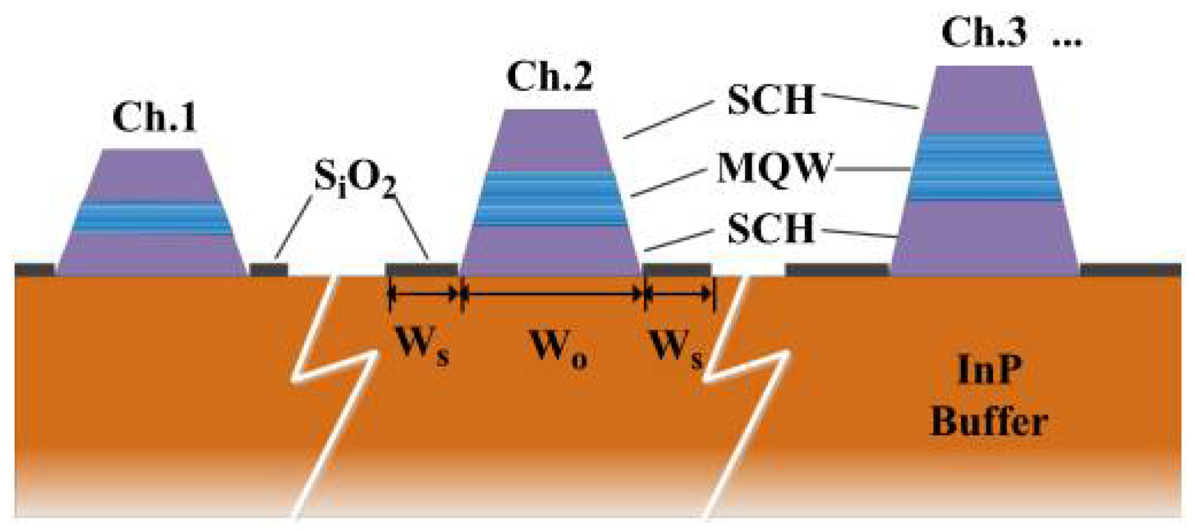
2.1. Parallel DFB Laser Array

2.1.1. Technical Principle, Advantages, and Disadvantages

A parallel DFB laser array is an array in which each laser has an independent waveguide and is coupled together by an S waveguide and a coupler, as shown in Figure 1.
The light emitted by the parallel DFB laser array needs to be coupled to a waveguide through photosynthetic wave devices to output. Various photosynthetic wave devices can be used such as a star coupler, directional coupler, multi-mode interference coupler (MMI), array waveguide grating (AWG), and micro-electro-mechanical system (MEMS). A star coupler can be provided with a high wavelength ratio, but its output power between channels is not uniform and produces high power loss. A directional coupler meets the very low insertion loss and reverse reflection requirements; however, the gap between waveguides is sub-micron in size, resulting in a fabrication process that is difficult to control accurately. Currently, directional couplers are commonly used in MMIs and AWGs, as shown in Figure 2.
Based on the principle of self-imaging, the MMI is not sensitive to wavelength and is suitable for the combined output of the multi-wavelength laser array. The process is relatively simple, but it has a low output power and large insertion loss, which increases with the increase in the number of channels. To solve these limitations, the MMI can be etched in both deep and shallow ridges, where the deep ridge can reduce insertion loss and crosstalk, and the shallow ridge has less end reflection.
The AWG is large and has both deep and shallow etching structures. The deep etching structure is small in size but is accompanied by a high insertion loss of greater than 5 dB in general. In contrast, the shallow etching structure has a relatively low insertion loss, generally less than 2 dB, but it requires a large bending radius, and the device is large. In InP-based chips, the AWG has wavelength sensitivity and as the wavelength of the laser changes, its insertion loss further increases.
Additionally, couplers are no longer required when using MEMS. In this configuration, a micromechanical mirror is added to the DFB laser array to achieve coupling. As MEMS tilt mirror achieves precise optical-mechanical alignment electronically, the tolerance is relaxed, and any deviation in the package can be corrected to reduce the package cost [9]. This method increases the device size compared to on-chip integration.
Figure 2. Schematic diagram of different couplers, (a) AWG [10] and (b) MMI [11]. © (a) Elsevier. Copyright 2015 optics communications. (b) Springer link. Copyright 2013 Science China Information Sciences.
Crystals 12 01006 g002
In terms of coupling stability, consider a system of N coupled semiconductor lasers described in dimensionless form by the following coupled-mode equations [12]:
d Y j d t = ( 1 i α ) Z j Y j + i η
T d Z j d t = P Z j   ( 1 + 2 Z j ) | Y j | 2
where Y j and Z j are defined as the normalized electrical field amplitude and normalized excess carrier density in the j th laser in sequence, respectively. t is measured in units of the photon lifetime τ p . T is the ratio between the carrier recombination time and photon lifetime, and is typically large. P is the normalized excess pumping current for a single laser above the threshold, α is defined as the linewidth enhancement factor, and η is the coupling constant between lasers, which represents the coupling difficulty and coupling strength required to obtain a stable in-phase solution.
If the lasers are coupled in parallel mode, the coupling term Y k in Equation (1) includes all the elements in the array except k = j . Then,
Y k = K = 1 n Y k , k j
It is convenient to reformulate Equations (1) and (2) in terms of the amplitude and phase of the electrical field. When Y j = E j exp ( i φ j ) is introduced, Equations (1) and (2) become
d E j d t = Z j E j η [ E k sin ( φ k φ j ) ]
T d Z j d t = P Z j ( 1 + 2 Z j ) E j 2
d φ j d t = α Z j + η E j 1 [ E k cos ( φ k φ j ) ]
For parallel coupling, from the characteristic equation [12], use
η > η p 2 α P 2 ( 1 + 2 P ) N
We will discuss this equation in detail in the next section when η is derived in a series array.
Technical advantage: the current DFB laser arrays are connected in parallel, meaning multiple DFB lasers are designed to be arranged in parallel and are coupled to a multimode interference combiner through a passive S-type waveguide. The advantage of this design is that its fabrication is relatively simple, only the fabrication of a single DFB laser and its couplings are considered, the mutual influence between the lasers is small, and the single-mode stability is high, and the tuning scheme is simple.
Technical disadvantage: during the coupling process, the output optical power encounters large losses, which is particularly critical for DFB lasers with an output wavelength of 1550 nm; therefore, an integrated optical amplifier (SOA) is often required. Moreover, as the number of lasers increases, the complexity and loss of parallel DFB laser arrays gradually increase when combining waves, the area occupied by the S-type passive waveguide increases, and the integrated optical amplifier will further add to the chip size, which is not conducive to the performance and integration of the chip, and also increases the total required current [13].
At present, for parallel DFB laser arrays, the main problem is that it is difficult to achieve low coupling loss and volume reduction simultaneously, which requires a higher output optical power of the laser or a coupling mode with lower loss.

2.1.2. Main Research Progress and Status

A parallel DFB laser array was manufactured for the first time in 1984 [14] and has made great improvements in various aspects of performance over the years. Currently, in laboratory preparation and commercial application, DFB laser arrays are still mainly connected in parallel. This method can integrate 16 or more DFB lasers, covering C-band, L-band, or O-band, and is suitable for coarse wavelength-division multiplexing (CWDM) systems and dense wavelength-division multiplexing (DWDM) systems.
For DWDM systems, the parallel DFB laser array can achieve a channel spacing of 0.8 nm [15], which is difficult to achieve by other structures such as series and series–parallel combinations. However, at the same time, the coupling loss of a parallel DFB laser array increases when the number of integrated lasers increases. Additionally, the problem of large volume after the integration of the MMI and AWG has not been solved. One possible solution to this problem may be to manufacture smaller combination devices.

2.2. Series DFB Laser Array

2.2.1. Technical Principle, Advantages and Disadvantages

To reduce the coupling difficulty and power loss of the laser array, a series DFB laser array is introduced, and its structure is shown in Figure 3. The technological process combines several DFB lasers in series such that all the DFB lasers are on the same waveguide. Thus, the laser array need not be laterally coupled, which avoids power losses during the coupling process, effectively reduces the chip size, and improves integration. However, in a tandem DFB laser array, the single-mode stability and wavelength accuracy of a single laser are easily affected by reflections from other lasers, resulting in poor beam quality and wavelength shift. When the wavelength spacing is less than 100 GHz (0.8 nm), grating crosstalk causes mode hopping. Using linear-chirped gratings to perform multiple π-phase shifts in a full cavity is an effective method for reducing crosstalk and suppressing side modes.
In a series DFB laser array, the wavelength spacing between the lasers is generally large, which requires a large temperature or current range to be tuned to cover all the desired wavelengths. Although, an excessive temperature or current tuning range many lead to device failure. Furthermore, decreases in the output power affects the reliability of the device. To reduce the influence of reflection, the phases of Bragg gratings in different lasers can be designed, and phase-shift gratings can be introduced between lasers to realise single longitudinal mode lasing.
In terms of coupling stability, if the lasers are coupled in series, the coupling stability is mainly affected by the two neighboring lasers. Consider a loop configuration and the coupling term Y k in Equation (1) given by
Y k = Y j + 1 + Y j 1
From the characteristic equation [12]
η > η c ( n ) = α P 2 ( 1 + 2 P ) sin 2 ( π n N )
The largest of all the η c ( n ) corresponds to the wave number n = 1 . Thus, it is required that
η > η s α P 2 ( 1 + 2 P ) sin 2 ( π n N )
By Equations (8) and (11), the critical coupling strengths η s and η p have been verified to be identical if N = 3 , since series coupling and parallel coupling are the same for three coupled lasers in a ring configuration. If N > 3 , η s becomes larger than η p . Thus, series coupling requires a larger value of the coupling strength q to have stable in-phase solutions.
At present, the number of DFB lasers that can be integrated into a series array is far less than that of a parallel array, and generally only 3–4 DFB lasers can be integrated with a channel spacing generally above 2 nm. For the series DFB laser array, it is easy to achieve a small volume, but methods to integrate more lasers, and ensure the single longitudinal mode and beam quality have not yet been developed.

2.2.2. Main Research Progress and Status

In a series DFB laser array, the number of lasers increases linearly as the required tuning range increases, which leads to an increasing length of the chip structure. By means of the shared grating sections of laser sections, that is, laser 1 passes through grating 1 and grating 2, laser 2 passes through grating 2 and grating 3, and laser N shines through grating N and grating N + 1, so that the total cavity length is significantly shortened, up to 40% in the array composed of 5 lasers [17].
In a series DFB laser array, the single-mode stability and wavelength reliability are poor due to the reflection of Bragg gratings in other lasers, especially when the wavelength spacing is very small. Lateral resonant modes can be suppressed by designing π phase shifts in the middle of each segment, and by inserting two mirrors on both ends of the laser to provide compensated reflection for both channels [18,19]. On this basis, a three-stage design was adopted to suppress the side mode by optimizing the current distribution and improving the priority of the dominant mode [20].
In 2021, Xiangfei et al. [21,22] proposed a tunable series-connected distributed feedback multi-wavelength laser array (DFB-MLA) based on reconstruction equivalent chirp (REC) technology. Its wavelength spacing was 2.4 nm and the SMSR was greater than 40 dB. The structure of the heat sink block was optimized for fast, continuous wavelength tuning.

2.3. Series–Parallel Combined DFB Laser Array

2.3.1. Technical Principle, Advantages, and Disadvantages

Regardless of a series or parallel onefold scheme of the DFB laser array, an increase in the number of lasers should consequently increase the difficulty of ensuring a single-mode output and low power loss. Therefore, when the number of integrated lasers is large, the use of a series or parallel structure alone makes the chip structure long and narrow, leading to difficulties when packaging. Therefore, a series–parallel combination is required.
At present, the series–parallel combination scheme is relatively new, and difficult to implement because it experiences the disadvantages of both types of arrays simultaneously. Nevertheless, it is still expected to become a popular topic in DFB laser array research.

2.3.2. Main Research Progress and Status

The series–parallel combination of a DFB laser array is not frequently implemented, but it may be the future development direction. In 2020, Xiangfei et al. [23,24] fabricated a 4 × 4 16-channel series–parallel DFB laser array that achieved 48 channels with a spacing of 100 GHz near 1550 nm and a temperature adjustment range below 20 °C. Compared with the series-only configuration, this matrix configuration reduces the potential interference from adjacent lasers, which reduces the overall power loss compared with the parallel-only configuration.

3. Implementation Method

The wavelength of the DFB laser is related to the refractive index of the active region and grating spacing, as shown in Equation (11). When fabricating a DFB laser array in which each DFB laser has a different emission wavelength, the fabrication methods can be divided into two categories: changing the grating structure and index of refraction modulation, and is represented as follows:
λ = 2 n e f f   Λ m
where λ is the lasing wavelength, n e f f is the effective index, Λ is the grating period, and m is the order of the grating.

3.1. Changing the Grating Structure

In the fabrication process of DFB laser arrays, various advanced fabrication methods are used to ensure the gratings of each laser have different periods. DFB laser arrays with different emission wavelengths can be fabricated based on one-time epitaxy of the same active region. Such technologies include electron-beam lithography, nano imprints, and REC technology.

3.1.1. Fabrication Methods

Electron Beam Lithography

  • Technical Principle
Electron beam lithography (EBL) is a lithography technique with the current highest known resolution, which can reach less than 10 nm. Currently, direct-write electron-beam lithography is primarily used. A focused electron beam bombards the photoresist to form the required pattern and scans, point by point, by moving and switching the electron beam to obtain the required grating structure.
2.
Technical Advantages and Disadvantages
Technical advantages: EBL has high precision, its direct point-by-point scanning does not require a photolithography mask, it can produce highly complex patterns, diffraction effects are negligible since the electron beam has a short wavelength, it supports dry etching rather than wet etching, it is easier to fabricate high-quality nanostructures, and can be used in high-precision processing of micro-nano electronic and optoelectronic devices.
Technical disadvantages: Owing to the high maintenance cost of EBL equipment, the need to write grating lines one by one leads to an extremely slow etching rate. Therefore, it is expensive and time consuming, and it is difficult to apply to the large-scale manufacturing of lasers and arrays. At the same time, EBL also has blanking or deflection errors and splicing errors, and only 35% of the lasers can be controlled within a range of ±0.2 nm [25]. Processes associated with EBL can generate errors of up to 3 nm [26]. Therefore, it is difficult to ensure the yield of this method when fabricating DFB laser arrays with small channel spacing.
3.
Main Research Progress and Status
EBL is a new lithography technology developed from the scanning electron microscope. Since the 1970s, it has been widely used in semiconductor integrated circuit manufacturing. Due to its slow processing speed, it is often used to manufacture application-specific integrated circuit (ASIC) with quick turn-around times and repeatable optical frames that require extremely high precision [27]. It has also been applied to laser grating manufacturing.
In the fabrication of the DFB laser array, a large number of studies have used electron beam lithography to fabricate grating structures [15,28,29,30,31,32,33,34,35], and the results are shown in Table 1. However, throughput capability, the most important problem of electron beam lithography in industrial applications, has not yet been solved. Hence, this technology is still mainly used in the laboratory and in the industry to build very small structures.

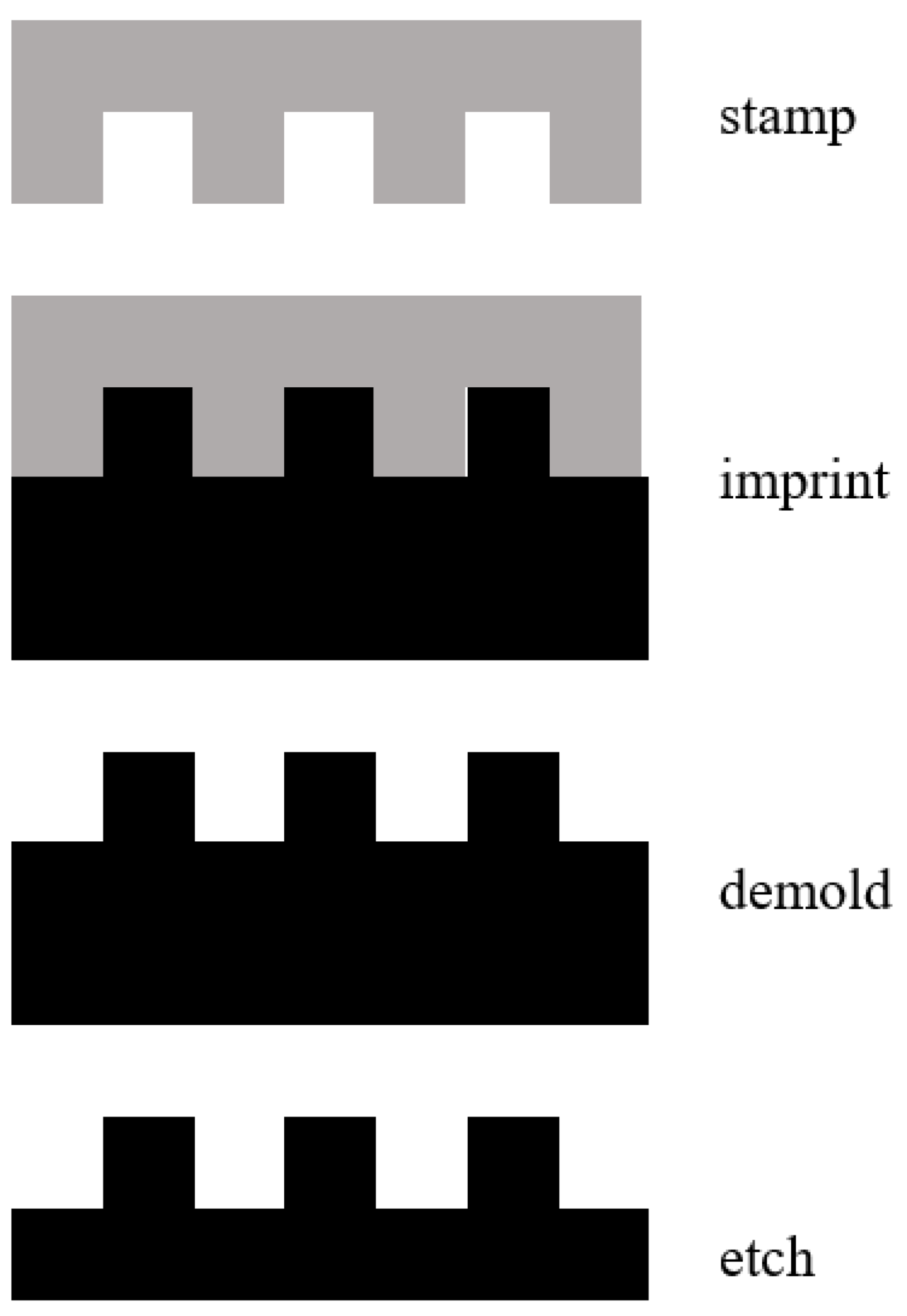
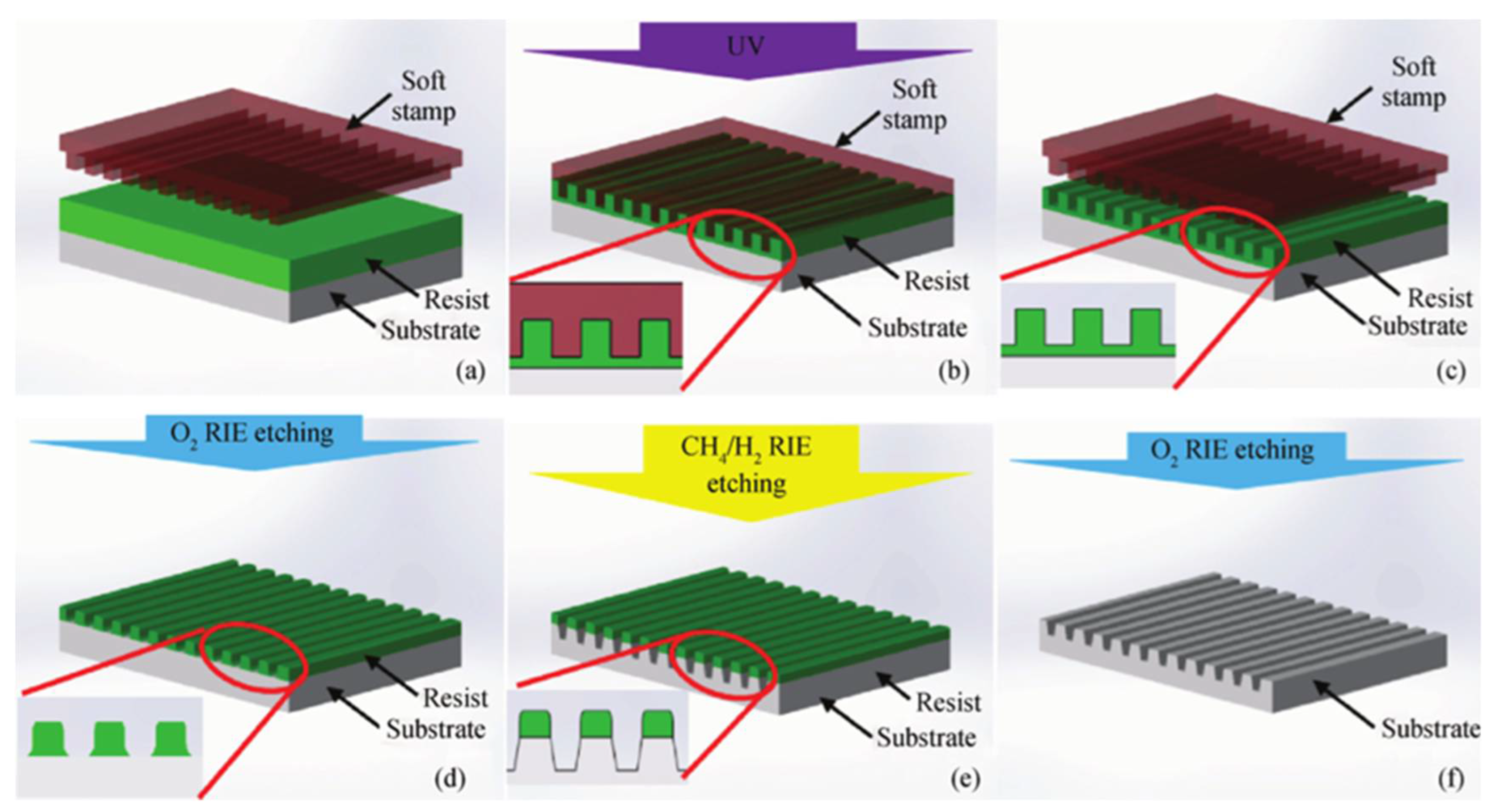
Nano-Imprint Lithography

  • Technical Principle
Nanoimprint lithography (NIL) is a pattern transfer technology; under pressure or heat or UV assisted action, the pattern on the template is transferred to the resist, the resist on the substrate to produce thickness difference, and then by etching the pattern transferred to the substrate. NIL is a promising, high-resolution, low-cost, nanoscale replication patterning technology.
The NIL pattern transfer technology process is illustrated in Figure 4, and is as follows: a film is created by spin-coating a resist onto a substrate, and the film is heated to vitrification. Subsequently, specific pressure is applied to imprint the pattern from the resist-coated substrate to the mold. Afterward, the mold is exposed to heat, UV light, or other elements to solidify the pattern. Finally, the mold and the pattern are separated and the pattern resist is left on the substrate, completing the photonic lithography process. DFB lasers with different grating periods can be prepared by imprinting templates of different shapes using this technique.
2.
Technical Advantages and Disadvantages
Technical advantages: NIL technology combines the advantages of EBL and holographic lithography and has the additional advantages of ultra-high resolution, easy mass production, low cost, fast speed, and high consistency. The imprint template is generally manufactured using high-precision EBL and can be used multiple times, thus significantly reducing costs. NIL technology changes the resist by imprinting instead of holographic lithography; therefore, its resolution is not affected by light diffraction, scattering, reflection, etc. Lithography pattern defects are suitable for large-scale manufacturing processes.
Technical disadvantages: during small-scale manufacturing, the cost of NIL technology is high owing to the high production cost of the imprint template. During the production process, the imprint template and the photoresist can easily lead to pattern defects, thereby decreasing precision. The mechanical brittleness of the InP substrate and the temperature difference between the substrate and the imprint template in hot imprinting results in nanoimprinting requiring a very refined process to ensure a good yield.
3.
Main Research Progress and Status
NIL technology mainly includes thermal and UV embossing.
Thermal NIL was first proposed by Chou in 1995 [37] and has been widely spread in the manufacturing process of optoelectronic devices such as gratings, microrings, and photonic crystals. At present, this technology is widely used in the fabrication of semiconductor laser gratings, which is a promising DFB laser array grating manufacturing technology. Thermal embossing is simple; however, the heating and cooling durations are long and time consuming, the thermoplastic polymer is prone to thermal expansion and contraction during the heating and cooling process, and the dimensional stability is poor, which easily leads to distortion of the copied graphics. This technique can be improved by employing laser-assisted direct imprinting [38].
There are two main challenges in laser grating thermal NIL. (1) The imprint process is very delicate because of the mechanical brittleness of the InP substrate and the thermal mismatch between the substrate and Si imprint. (2) Subsequent processing requires specific imprint compressive thicknesses after plate making, the crystallographic direction of the substrate, and arrangement of the grating for plate making [39].
Therefore, for thermal NIL, the most important physical properties of the mask are the thermal expansion coefficient and Poisson’s ratio. In addition, properties such as hardness, durability, and surface roughness should also be considered. Material selection includes Si, SiO2, SiC, Si3N4, metal, and sapphire [40].
For InP substrates, current studies have shown that the maximum pressure in hot stamping technology does not exceed 3 bar [39].
UV imprinting is also known as room-temperature imprinting. In 1996, UV nanoimprint lithography was designed by introducing a low viscosity UV-curable polymer layer to improve the fluidity of the imprint material [41]. The process involves cross-linking the polymer by UV light on a transparent die after embossing on a UV-cured layer, which significantly reduces the pressure during nano embossing without the need for high temperatures. Low temperature eliminates deformation errors and graphic distortions caused by differences in the thermal expansion coefficient, and low pressure makes the process more likely to succeed on more brittle substrates such as InP and GaAs. Therefore, the technology is more suitable for PICs and manufacturing DFB laser arrays.
UV soft-printing technology is used to fabricate gratings, as shown in Figure 5 [42]. Compared with nano-imprinting directly using hard master printing, the pattern quality is better, especially in the case of surface unevenness that often occurs during multiple epitaxy processes. The specific implementation method is as follows. First, a soft imprint is prepared by imprinting a hard master composed of Si on a flexible intermediate polymer imprint (IPS Obducat AB) using thermal NIL. Next, the epitaxial wafer is carefully cleaned and coated with a layer of UV-curable resist (stuc-220, Obducat AB). Home-made mechanical tools are used to precisely align the soft-printed grating pattern with the grating segments on the wafer. The pattern is then transferred onto the epitaxial structure using an intermediate polymer imprinting (IPS) process by performing simultaneous thermal and UV imprinting processes. After cleaning the residual resist using an oxidative reactive ion etching (RIE) process, inductively coupled plasma (ICP) RIE is used to prepare the grating, and O2 plasma is used to remove the mask.
However, as there is no heating or cooling process, polymer bubbles cannot be eliminated, which greatly affects the graphics. An improvement in this process uses a step-flash or thermal UV imprint technology that combines UV imprinting with stepping technology or thermal imprints, respectively. In this process, the corrosion inhibitor is the key problem. The selected resist must maintain low viscosity at room temperature, be able to cure under UV irradiation with minimal shrinkage to maximize pattern accuracy and be released from the mask after curing to adhere to the substrate. A modified poly-dimethyl-siloxane (PDMS) soft stamp has been used to reduce pattern deformation and residual layer thickness, and the residual layer thickness has been reduced by 50% [43].
NIL technology is also widely used in the fabrication of DFB lasers and array gratings, and there have been many recent innovations. Compared with Si substrates used in large-scale integrated circuits, compound semiconductor substrates such as GaAs and InP often have large thickness fluctuations, resulting in the uneven thickness of the residual layer in the imprinting area when NIL technology is applied, ultimately resulting in the graph changes. To solve this problem, reverse NIL technology has been developed and is based on step-and-repeat imprinting named step and flash imprint lithography (SFIL), which can inhibit the uneven residual layer caused by substrate fluctuation [44].
In the NIL process, the duty cycle of gratings may change due to the deformation of the resist and the soft mode. However, when the grating angle is less than 3° and the duty cycle is between 0.4 and 0.6, the effect of error can be ignored, which can be easily achieved with SFIL technology [45].
In NIL, the imprint template is usually prepared using the EBL method, which provides better stability. In addition, during the pattern-transfer process using the NIL method, the resist is in direct contact with the stamp with little deformation. Therefore, NIL can smooth raster edges. This has important implications for the fabrication of high-quality lasers, which can reduce the spectral width of higher-order Fourier components owing to imperfect gratings.

3.1.2. Special Grating Design Reconstruction

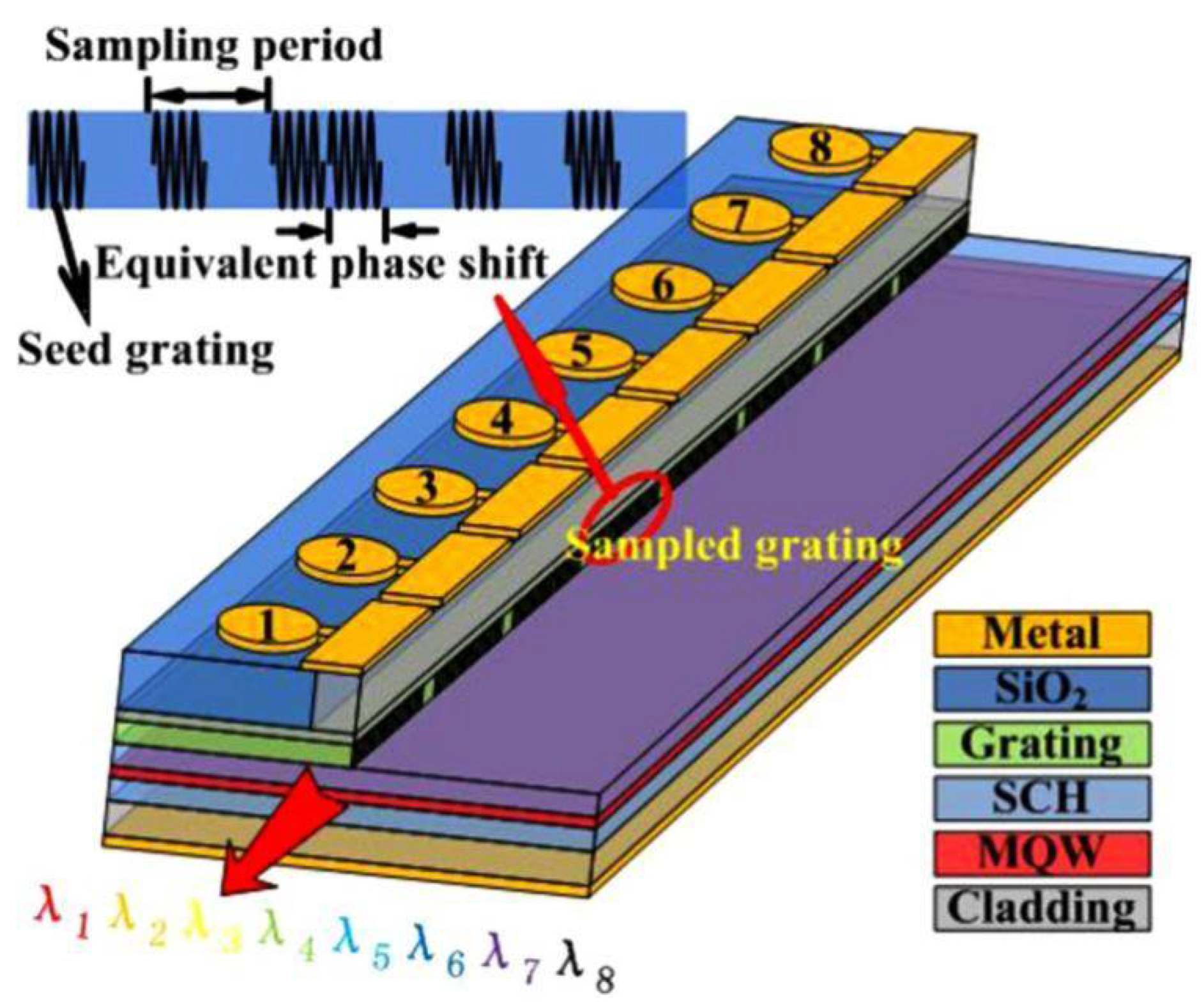
Reconstruction Equivalent Chirp

  • Technical Principle
The REC technique is based on the reflection response. By designing a sampling grating based on the sampling function, the chirp structure of the grating period that changes with position is obtained, and the function of the complex grating is realized effectively. The REC technique achieves equivalence with complex grating structures by fabricating specially designed sampling gratings that are superposed on a uniform gratings pattern. The REC technology utilizes sampled Bragg gratings (SBGs) to design and fabricate lasers and laser arrays with complex grating structures. By changing the sampling mode, an equivalent chirp (continuous variation) or equivalent displacement (discrete variation) of the grating neutron grating (Fourier component) can be generated. The Bragg wavelengths of the sub-ratings can also vary with the sampling period. Thus, various sub-grating with complex structures can be obtained by designing the sampling patterns in advance. The sampling period is usually a few microns and can be formed by ordinary photolithography [46].
According to Fourier analysis, the index modulation of a grating section with sampling period P and a basically uniform (seed) grating period Λ 0 can be expressed as [47]:
Δ n ( z ) = 1 2 Δ n s m F m exp ( j 2 π z Λ 0 + j 2 m π z P + φ ) + c . c
where Δ n s is the index modulation of the uniform seed grating, F m is the Fourier coefficient of the mth order sub-grating z is the position along the laser cavity, Λ 0 is the seed grating period, P is the sampling period, φ is the initial phase of the seed grating, m is the order of Fourier component, and usually the + 1 s t or 1 s t order sub-grating is used. The ± 1 s t order period can be expressed as,
1 Λ m = 1 Λ 0 + m P
Therefore, if the sampling period P is carefully designed for a suitable wavelength grid and each laser section with a specific wavelength is tuned by changing the chip temperature, a wide wavelength range can be covered and the wavelength tuning can be realized simultaneously. According to Equation (11), Λ can change by changing P to achieve different output wavelengths in different lasers.
2.
Technical Advantages and Disadvantages
Technical advantages: the REC technology can achieve complex grating structures through micron-scale sampling patterns. In the grating fabrication process, only two steps are required: holographic exposure of the uniform base (seed) grating and lithography of the sampling pattern. All other processes are the same as those used for conventional DFB lasers. Therefore, the manufacturing costs are low. The most important advantage of this technique is that it provides precise fabrication of periodic structures for precise control of wavelengths, and its accuracy is 100-fold higher than that of general theoretical methods [48].
Technical disadvantages: owing to different sampling periods, the phase of the cavity surface of the laser will change, which destroys the uniformity of the wavelength spacing of the laser array. To obtain a uniform wavelength separation, minimal reflection is required on both laser faces; however, this results in a high threshold current and low slope efficiency. Without a reflection-enhancing coating, the wavelength deviation of the laser array can reach approximately 1 nm [47]. In addition, the REC technique reduces the SMSR of side-mode sampling.
3.
Main Research Progress and Status
REC technology was initially proposed in fiber Bragg gratings [49] and has been applied to optical filters, fiber lasers, OCDMA en/decoders, and other important optical devices. Xiangfei et al. conducted extensive and in-depth research on the fabrication of DFB laser arrays using REC technology. REC technology in 2009 to fabricate a multi-wavelength DFB laser array, which attracted wide attention due to its low cost and simple method [50]. In 2012, they then made an 8-channel parallel DFB, with an error tolerance of approximately 520-fold higher than the previous array [48].
For the DFB laser array, because it integrates multiple DFB lasers, the yield drops sharply compared with a single DFB laser. The yield is a key issue in the fabrication of DFB laser arrays. The 60-channel DFB laser array produced by REC technology can control the wavelength error of 83% of the laser within ±0.20 nm and 93.5% of the laser within ±0.30 nm [51], greatly improving the yield. REC technology can not only be used in the manufacturing of parallel DFB laser arrays but also in the manufacturing of series DFB laser arrays [22] and series–parallel combined DFB laser arrays [52].

3.2. Index of Refraction Modulation

In the fabrication of DFB laser arrays, in addition to realizing different emission wavelengths by preparing gratings with different periods in different lasers, wavelength changes can also be achieved by changing the refractive index in different lasers. Such technologies include ridge width variation technology and selective area growth.

3.2.1. Ridge Width Variation Technology

Technical Principle

The systemic equivalent refractive index can be adjusted by adjusting the width of the ridge waveguide of the laser, according to Equation (12).

Technical Advantages and Disadvantages

Technical advantages: the process of changing the width of the laser waveguide is simple, and is suitable for manufacturing DFB laser arrays with narrow channel spacing.
Technical disadvantages: the scope of application is limited, the threshold value of the device is too wide and may cause the device to generate multiple transverse modes, the waveguide is too narrow, the series resistance is too high, the thermal effect is obvious, and it is difficult for the device to achieve consistent characteristics.

Main Research Progress and Status

Li et al. [53] proposed varying ridge widths to adjust the lasing wavelength of DFB laser arrays in 1996 and demonstrated that even if the ridge width was sufficient to support multiple lateral modes, single-mode lasers could be maintained. Therefore, the tuning range of the array could be increased without affecting the single-mode performance.
The method can be used to fabricate DFB laser arrays with very small channel spacing, which can reach 0.8 nm [54]. However, because the effective refractive index of the laser varies nonlinearly with the width of the ridge waveguide, and the width of the ridge waveguide cannot be too small (the machining accuracy is difficult to achieve) or too large (A high-order transverse mode is generated), the wavelength tuning range that can be achieved by this scheme is very limited.

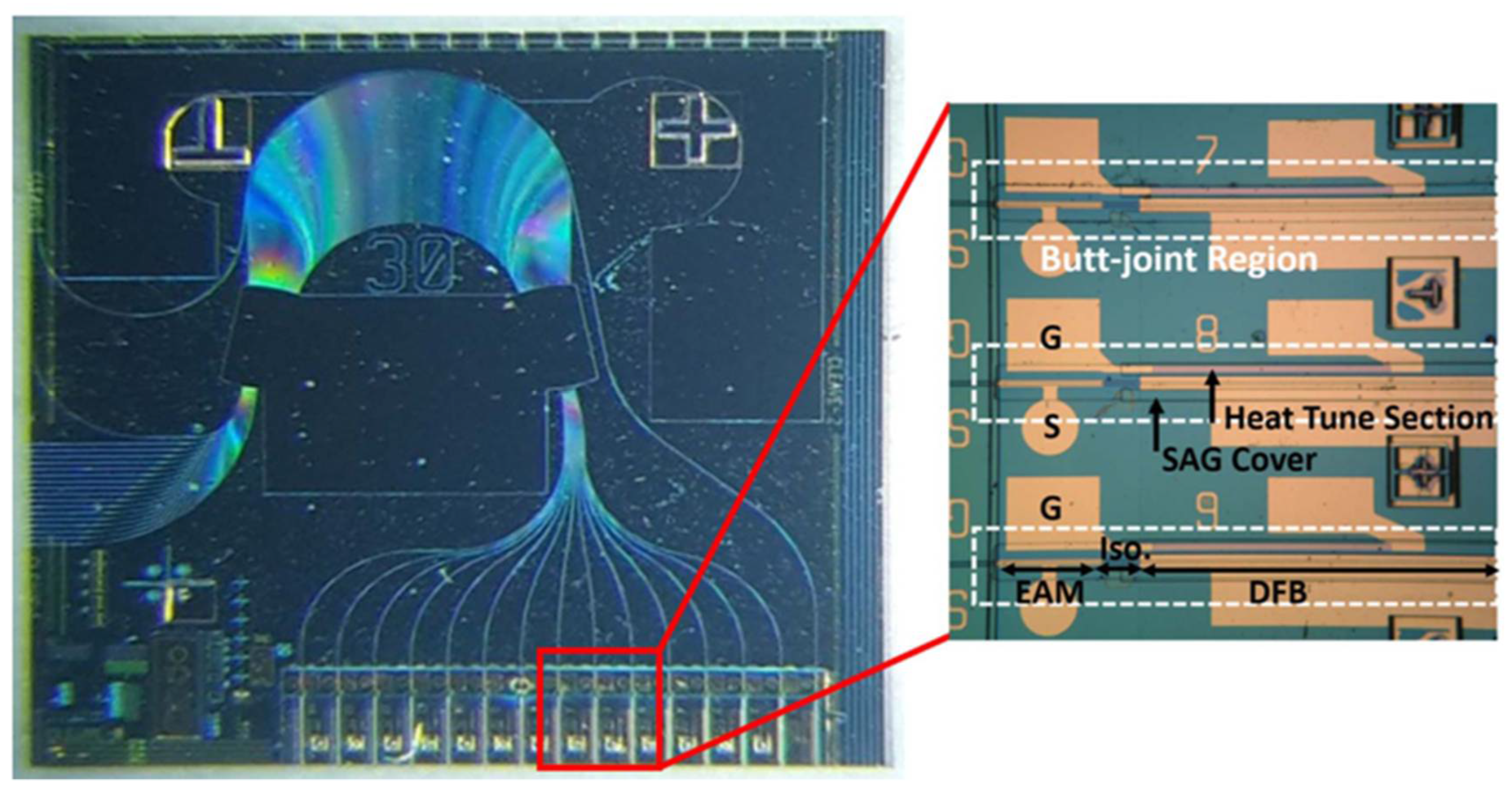
3.2.2. Selective Area Growth

Technical Principle

Selective area growth (SAG) is performed as follows: a series of mask stripes are fabricated on a substrate, and then epitaxial layers are grown in areas without mask stripes, as shown in Figure 6. In the SAG process, SiO2 mask stripes are formed on the substrate before the material is grown; thus, in the subsequent Metal–Organic Chemical Vapor Deposition (MOCVD) or Metal–Organic Vapor Phase Epitaxial Growth (MOPVE) process, the material is only grown where there are no mask stripes. In other words, SAG technology can be used to control the structural parameters of each laser active region, including the thickness and material composition, to change the refractive index of the laser active region, thereby changing the emission wavelength. The SAG technology can simultaneously control the multiple quantum well (MQWs) bandgap energy of the arrayed waveguide by changing the mask pattern’s dummy stripe width and the width of the outer mask [55]. By using an asymmetric mask, an almost linear shift in emission wavelength can be obtained. For MQWs, because the emission wavelength is sensitive to the thickness of the well, extensive wavelength tuning can be obtained in addition to refractive index changes.
The thickness enhancement factor of the selectively grown layer is affected by the geometry of the mask pattern, including mask width and pitch. By designing the geometry of the mask, precise control of the thickness of the active region and the waveguide layer can be achieved, and thus control of the effective index of refraction can be achieved to achieve different wavelengths in the laser array [56].
The SAG mechanism is generally considered to be the surface diffusion component and the vapor phase diffusion component. Surface diffusion refers to the molecular diffusion of reactants from the mask surface to the exposed surface, while vapor phase diffusion refers to the vertical and lateral diffusion of reactant molecules in the gas phase and adhesion to the exposed surface.
In general SAG modeling, surface diffusion is usually ignored because it only occurs within a few micrometers of the edge of the mask.
Vapor phase diffusion can be described by the gas-phase diffusion model, and its diffusion equation is [57]:
2 C x 2 + 2 C y 2 = 0
where C ( y , z ) is the vapor phase concentration.
Assuming no growth of material on the mask, and that the gas concentration just above the crystal surface in the exposed region between the masks remains constant at equilibrium [57]:
{ z = d ,   C = C y = y 0 2 + w , z = r s π ,   C = C c z = 0 ,   C = 0
where d is the height of the stagnant layer, y 0 is the width of the mask, and w is the distance between the masks. r s is the radius of the hemicylindrical structure of the grown SAG structure at the window. The value of r s is equivalent to the window width, w , and is assumed to be much smaller than y 0 to simplify the following formula.
Under this boundary condition, the solution of equation (14) is [57]:
C = A ln [ sin 2 ( π y 0 y ) + sinh ( π y 0 z ) ] 1 2 + B
where A and B are [57]:
A = C C c ln [ sinh ( π d y 0 ) ] ln [ sinh ( r s y 0 ) ] C C c ln [ y 0 r s sinh ( π d y 0 ) ]
B = C + A ln [ sinh ( π d y 0 ) ]
The growth rate v g can be expressed as [57]:
v g = v D g w π A r s = v D g π ( C C c ) w r s { ln [ sinh ( π d y 0 ) ] ln [ sinh ( r s y 0 ) ] }
where Dg is the diffusion coefficient of molecules in the vapor phase.
A s a limiting case, r s d and y 0 d ,
v g v D g ( C C c ) w r s d y 0
During the SAG growth process, the grown material generates a growth rate enhancement curve in the unmasked area, by formula (20), the growth rate is proportional to the width of the dielectric mask and inversely proportional to the square of the mask spacing. In addition, group III elements will have a certain compositional shift during growth, while group V elements will not; therefore, the SAG technique will lead to a certain degree of inhomogeneity [58].
The traditional MQW SAG technology forms a dielectric mask on the buffer substrate, and the selective region growth layer includes the lower separate confinement structure (SCH), MQW, and upper SCH layers. The difference is that in the new SAG technology, the buffer, lower SCH, and MQW layers are first grown on the substrate. Subsequently, mask strip pairs are formed on the MQW layer. In the following SAG process, only one upper SCH layer is grown, which effectively reduces the difficulty of the process by reducing the number of selectively grown layers. At the same time, SAG technology can be combined with EBL and REC technologies to achieve improved performance.

Technical Advantages and Disadvantages

Technical advantages: SAG technology is used to fabricate DFB semiconductor laser arrays because of its simplicity, low cost, and suitability for mass production. While forming a laser array, SAG can also be used for the integration of the laser array with other optical components, such as electro-absorption modulators (EAMs) [59].
Technical disadvantages: The SAG process requires good control of the epitaxial growth process and advanced technology. Additionally, it has low repeatability and it is difficult to guarantee the single longitudinal modulus rate, requiring other technologies to control it.

Main Research Progress and Status

SAG is widely used in the epitaxial growth of various semiconductor devices and was first applied in the preparation of the multi-wavelength DFB laser array in 1994 [60]. This method can prepare a DFB laser array with a wide wavelength span of up to 155 nm [61]. SAG technology is very flexible and can be used in combination with a variety of technologies. For example, gratings can be made using EBL based on SAG [62], and the width of ridge waveguides can be changed while SAG technology is used [63] or by combining SAG technology, and EBL technology, and reverse mesa ridge waveguide LD processing technology [64]. SAG technology can simultaneously integrate MMI, SOA, MOD, and other devices on the chip [65]. SAG technology can also be combined with bundled integrated waveguide (BIG) technology to obtain uniformly spaced multi-wavelength emission and low-loss passive waveguide materials in one MOCVD step, greatly simplifying the integrated fabrication of the array [66].
In the SAG process, the material layers affected by SAG include two SCH and MQW layers, which may affect the uniformity of the laser array [8]. Therefore, an improved SAG method has been proposed [67]. First, the buffer, low SCH, and MQW layers are grown on the substrate, and then the size is formed on the MQW layer, gradually changing mask–strip pairs. In the next step, only the upper SCH layer is grown, and only the thickness of the upper SCH layer is changed through the SAG mask to obtain different Bragg wavelengths. Materials including the SCH and MQW layers are very sensitive to different growth conditions; therefore, the wavelength spacing can be precisely controlled.
As the thickness of the material can be controlled with precision, SAG technology is especially suitable for fabricating laser arrays with small channel spacing, which can achieve good wavelength spacing uniformity. However, DFB lasers with a high single-longitudinal-mode rate are not guaranteed. Therefore, REC technology has been adopted to introduce an equivalent phase shift to ensure the single-mode laser output of the DFB laser [68].

4. Conclusions

In summary, the DFB laser array is among the most widely used and mature solutions in WDW. Compared with other lasers, its mode stability, high wavelength stability, and narrow linewidth make it stand out. The research on DFB laser arrays is also the most extensive. The multi-wavelength DFB laser array is a key component of the wavelength-division multiplexing system, and its manufacturing difficulties affect its mass production and use. This paper summarizes the structure and fabrication methods for multi-wavelength DFB laser arrays. At present, various DFB laser array structures and fabrication methods can still be improved. Finding a low-cost, high-yield, easy fabrication method, that can adopt a reasonable structure, are key factors to promote the further development of DFB laser arrays.
For DFB laser arrays, the main problems to be solved in the future are the wavelength accuracy and the wavelength spacing of different lasers. In particular for DWDM applications, the wavelength spacing of future DFB laser arrays may still be further reduced, which will put forward higher requirements for technical accuracy. On the one hand, we need to continue to improve the existing technologies such as EBL, NIL, and other processes; on the other hand, in the design of gratings, active regions, waveguides, etc., such as REC and SAG, it is also necessary to further reduce errors. In addition, the DFB laser arrays currently used in optical communications are mainly InP based, which is difficult to match with standard integrated circuit processes. In the future, emerging multi-wavelength WDM sources based on Si photonics are also very expected.

Author Contributions

Conceptualization, S.N. and Y.S.; methodology, C.Q. and Y.L.; validation, P.J., Y.C. and Y.W. (Ye Wang); formal analysis, Y.S. and L.Z.; investigation, Y.S., C.Q., Y.W. (Yubing Wang) and Y.L.; resources, S.N., Y.W. and Y.S.; writing—original draft preparation, S.N.; writing—review and editing, L.Z. and Y.S.; supervision, Y.C. and L.L.; project administration, Y.N.; funding acquisition, L.Q. and L.W. All authors have read and agreed to the published version of the manuscript.

Funding

This work is supported by the National Science and Technology Major Project of China (2021YFF0700500); National Natural Science Foundation of China (NSFC) (61904179, 62090051, 62090052, 62090054, 11874353, 61935009, 61934003, 62004194); Science and Technology Development Project of Jilin Province (20200401069GX, 20200401062GX, 20200501006GX, 20200501007GX, 20200501008GX); Key R&D Program of Changchun [21ZGG13, 21ZGN23]; Innovation and entrepreneurship Talent Project of Jilin Province [2021Y008]; Special Scientific Research Project of Academician Innovation Platform in Hainan Province (YSPTZX202034), and “Lingyan” Research Program of Zhejiang Province (2022C01108).

Institutional Review Board Statement

Not applicable.

Informed Consent Statement

Not applicable.

Data Availability Statement

Not applicable.

Conflicts of Interest

The authors declare no conflict of interest.

References

  1. Nesset, D. NG-PON2 Technology and Standards. J. Lightwave Technol. 2015, 33, 1136–1143. [Google Scholar] [CrossRef]
  2. Coldren, L.A.; Fish, G.A.; Akulova, Y.; Barton, J.S.; Johansson, L.; Coldren, C.W. Tunable semiconductor lasers: A tutorial. J. Lightwave Technol. 2004, 22, 193–202. [Google Scholar] [CrossRef]
  3. Chan, C.K.; Sherman, K.L.; Zirngibl, M. A fast 100-channel wavelength-tunable transmitter for optical packet switching. IEEE Photonics Technol. Lett. 2001, 13, 729–731. [Google Scholar] [CrossRef]
  4. Wang, Y.Y.; Lin, K.L.; Fang, T.; Chen, X.F. A tunable SFP optical module based on DFB laser array integrated with a SOA. Optoelectron. Devices Integr. VII 2018, 10814, 153–158. [Google Scholar] [CrossRef]
  5. Kudo, K.; Morimoto, T.; Yashiki, K.; Sasaki, T.; Yokoyama, Y.; Hamamoto, K.; Yamaguchi, M. Wavelength-selectable microarray light sources of multiple ranges simultaneously fabricated on single wafer. Electron. Lett. 2000, 36, 745–747. [Google Scholar] [CrossRef]
  6. Lee, S.L.; Pukhrambam, P.D. Wavelength division multiplexing laser arrays for applications in optical networking and sensing: Overview and perspectives. Jpn. J. Appl. Phys. 2018, 57, 08PA03. [Google Scholar] [CrossRef]
  7. Luo, Y.Q.; Roberts, H.; Grobe, K.; Valvo, M.; Nesset, D.; Asaka, K.; Rohde, H.; Smith, J.; Wey, J.S.; Effenberger, F. Physical Layer Aspects of NG-PON2 Standards-Part 2: System Design and Technology Feasibility. J. Opt. Commun. Netw. 2016, 8, 43–52. [Google Scholar] [CrossRef]
  8. Liang, S.; Lu, D.; Zhao, L.J.; Zhu, H.L.; Wang, B.J.; Zhou, D.B.; Wang, W. Fabrication of InP-based monolithically integrated laser transmitters. Sci. China Inf. Sci. 2018, 61, 080405. [Google Scholar] [CrossRef]
  9. Pezeshki, B.; Vail, E.; Kubicky, J.; Yoffe, G.; Heanue, J.; Epp, P.; Rishton, S.; Ton, D.; Faraji, B.; Emanuel, M.; et al. 20-mW widely tunable laser module using DFB array and MEMS selection. IEEE Photonics Technol. Lett. 2002, 14, 1457–1459. [Google Scholar] [CrossRef]
  10. Pan, P.; An, J.M.; Zhang, J.S.; Wang, Y.; Wang, H.J.; Wang, L.L.; Yin, X.J.; Wu, Y.D.; Li, J.G.; Han, Q.; et al. Flat-top AWG based on InP deep ridge waveguide. Opt. Commun. 2015, 355, 376–381. [Google Scholar] [CrossRef]
  11. Zhu, H.L.; Ma, L.; Liang, S.; Zhang, C.; Wang, B.J.; Zhao, L.J.; Wang, W. InP based DFB laser array integrated with MMI coupler. Sci. China Technol. Sci. 2013, 56, 573–578. [Google Scholar] [CrossRef]
  12. Li, R.D.; Erneux, T. Stability Conditions for Coupled Lasers—Series Coupling Versus Parallel Coupling. Opt. Commun. 1993, 99, 196–200. [Google Scholar] [CrossRef]
  13. Macomber, S.H.; Mott, J.S.; Schwartz, B.D.; Setzko, R.S. Curved-grating, surface-emitting DFB lasers and arrays. In-Plane Semicond. Lasers Ultrav. Midinfrared 1997, 3001, 42–54. [Google Scholar] [CrossRef]
  14. Okuda, H.; Hirayama, Y.; Furuyama, H.; Uematsu, Y. Simultaneous Cw Operation of 5-Wavelength Integrated Gainasp-Inp Dfb Laser Array with 50-a Lasing Wavelength Separation. Jpn. J. Appl. Phys. Part 2 Lett. 1984, 23, L904–L906. [Google Scholar] [CrossRef]
  15. Hou, L.P.; Tang, S.; Marsh, J.H. Monolithic DWDM source with precise channel spacing. J. Semicond. 2021, 42, 042301. [Google Scholar] [CrossRef]
  16. Li, L.Y.; Tang, S.; Lu, J.; Shi, Y.C.; Cao, B.L.; Chen, X.F. Study of cascaded tunable DFB semiconductor laser with wide tuning range and high single mode yield based on equivalent phase shift technique. Opt. Commun. 2015, 352, 70–76. [Google Scholar] [CrossRef]
  17. Zhao, Y.; Shi, Y.C.; Li, J.; Liu, S.P.; Xiao, R.L.; Li, L.Y.; Lu, J.; Chen, X.F. A Cascaded Tunable DFB Semiconductor Laser With Compact Structure. IEEE J. Quantum Electron. 2018, 54, 2200111. [Google Scholar] [CrossRef]
  18. Sun, Z.X.; Xiao, R.L.; Zhao, Y.; Lv, G.; Su, Z.R.; Shi, Y.C.; Chen, X.F. Design of Four-Channel Wavelength-Selectable In-Series DFB Laser Array With 100-GHz Spacing. J. Lightwave Technol. 2020, 38, 2299–2307. [Google Scholar] [CrossRef]
  19. Sun, Z.X.; Xiao, R.L.; Zhao, Y.; Dai, P.; Lv, G.; Su, Z.R.; Shi, Y.C.; Chen, X.F. Design of Wavelength-selectable In-series DFB Laser Array Based on Chirped Bragg Grating. In Proceedings of the 2019 Asia Communications and Photonics Conference (ACP), Chengdu, China, 2–5 November 2019. [Google Scholar]
  20. Sun, Z.X.; Xiao, R.L.; Su, Z.R.; Liu, K.; Hu, Z.Y.; Dai, P.; Lu, J.; Zheng, J.L.; Zhang, Y.S.; Shi, Y.C.; et al. High Single-Mode Stability Tunable In-Series Laser Array With High Wavelength-spacing Uniformity. J. Lightwave Technol. 2020, 38, 6038–6046. [Google Scholar] [CrossRef]
  21. Sun, Z.X.; Xiao, R.L.; Su, Z.R.; Liu, K.; Lv, G.; Xu, K.; Fang, T.; Shi, Y.C.; Chiu, Y.J.; Chen, X.F. Experimental Demonstration of Wavelength-tunable In-Series DFB Laser Array with 100-GHz Spacing. IEEE J. Sel. Top. Quantum Electron. 2022, 28, 1500308. [Google Scholar] [CrossRef]
  22. Dai, P.; Sun, Z.X.; Chen, Z.; Lu, J.; Wang, F.; Tong, H.; Xiao, R.L.; Chen, X.F. Enhanced Tuning Performance of In-Series REC-DFB Laser Array. IEEE Photonics Technol. Lett. 2021, 33, 1337–1340. [Google Scholar] [CrossRef]
  23. Su, Z.; Xiao, R.; Sun, Z.; Yang, Z.; Chen, X. 48 channels 100-GHz tunable laser by integrating 16 DFB lasers with high wavelength-spacing uniformity. arXiv 2020, arXiv:2001.01178. [Google Scholar]
  24. Liu, K.; Wang, Q.M.; Lin, K.L.; Fang, T.; Chen, X.F. Fast wavelength-switching DFB laser array with 16 channels based on the REC technology. Semicond. Lasers Appl. X 2020, 11545, 42–48. [Google Scholar] [CrossRef]
  25. Lee, T.P.; Zah, C.E.; Bhat, R.; Young, W.C.; Pathak, B.; Favire, F.; Lin, P.S.D.; Andreadakis, N.C.; Caneau, C.; Rahjel, A.W.; et al. Multiwavelength DFB laser array transmitters for ONTC reconfigurable optical network testbed. J. Lightwave Technol. 1996, 14, 967–976. [Google Scholar] [CrossRef]
  26. Zanola, M.; Strain, M.J.; Giuliani, G.; Sorel, M. Post-Growth Fabrication of Multiple Wavelength DFB Laser Arrays With Precise Wavelength Spacing. IEEE Photonics Technol. Lett. 2012, 24, 1063–1065. [Google Scholar] [CrossRef]
  27. Okazaki, S. High resolution optical lithography or high throughput electron beam lithography: The technical struggle from the micro to the nano-fabrication evolution. Microelectron. Eng. 2015, 133, 23–35. [Google Scholar] [CrossRef]
  28. Adachi, K.; Shinoda, K.; Kitatani, T.; Fukamachi, T.; Matsuoka, Y.; Sugawara, T.; Tsuji, S. 25-Gb/s Multichannel 1.3-mu Surface-Emitting Lens-Integrated DFB Laser Arrays. J. Lightwave Technol. 2011, 29, 2899–2905. [Google Scholar] [CrossRef]
  29. Tsuruoka, K.; Kobayashi, R.; Ohsawa, Y.; Tsukuda, T.; Kato, T.; Sasaki, T.; Nakamura, T. Four-channel 10-Gb/s operation of AlGaInAs-MQW-BH-DFB-LD array for 1.3-mu m CWDM systems. IEEE J. Sel. Top. Quantum Electron. 2005, 11, 1169–1173. [Google Scholar] [CrossRef]
  30. Becker, A.; Sichkovskyi, V.; Bjelica, M.; Rippien, A.; Schnabel, F.; Kaiser, M.; Eyal, O.; Witzigmann, B.; Eisenstein, G.; Reithmaier, J.P. Widely tunable narrow-linewidth 1.5 mu m light source based on a monolithically integrated quantum dot laser array. Appl. Phys. Lett. 2017, 110, 181103. [Google Scholar] [CrossRef]
  31. Tang, S.; Hou, L.P.; Chen, X.F.; Marsh, J.H. Multiple-wavelength distributed-feedback laser arrays with high coupling coefficients and precise channel spacing. Opt. Lett. 2017, 42, 1800–1803. [Google Scholar] [CrossRef] [Green Version]
  32. Li, A.K.; Wang, J.; Sun, C.Z.; Wang, Y.Q.; Yang, S.H.; Xiong, B.; Luo, Y.; Hao, Z.B.; Han, Y.J.; Wang, L.; et al. 1.3 mu m 10-Wavelength Laterally Coupled Distributed Feedback Laser Array with High-Duty-Ratio Gratings. Phys. Status Solidi A Appl. Mater. Sci. 2019, 216, 1800490. [Google Scholar] [CrossRef] [Green Version]
  33. Wang, Q.C.; Wang, J.; Sun, C.Z.; Xiong, B.; Luo, Y.; Hao, Z.B.; Han, Y.J.; Wang, L.; Li, H.T.; Yu, J.D. A Directly Modulated Laterally Coupled Distributed Feedback Laser Array Based on SiO2 Planarization Process. Appl. Sci. 2021, 11, 221. [Google Scholar] [CrossRef]
  34. Zhao, G.Y.; Liu, G.H.; Liu, C.; Lu, Q.Y.; Guo, W.H. Monolithically Integrated Directly Modulated ADR-DFB Laser Array in the O-Band. IEEE Photonics Technol. Lett. 2019, 31, 1495–1498. [Google Scholar] [CrossRef]
  35. Dudelev, V.V.; Mikhailov, D.A.; Andreev, A.D.; Kognovitskaya, E.A.; Sokolovskii, G.S.J.Q.E. Tunable single-frequency radiation source based on an array of DFB lasers for the spectral range of 1.55 μm. Quantum Electron. 2019, 49, 1158–1162. [Google Scholar] [CrossRef]
  36. Oohashi, H.; Shibata, Y.; Ishii, H.; Kawaguchi, Y.; Kondo, Y.; Yoshikuni, Y.; Tohmori, Y. 46.9-nm wavelength-selectable arrayed DFB lasers with integrated MMI coupler and SOA. In Proceedings of the 2001 International Conference on Indium Phosphide and Related Materials, Nara, Japan, 14–18 May 2001; pp. 575–578. [Google Scholar] [CrossRef]
  37. Chou, S.Y.; Krauss, P.R.; Renstrom, P.J. Imprint lithography with 25-nanometer resolution. Science 1996, 272, 85–87. [Google Scholar] [CrossRef]
  38. Chou, S.Y.; Keimel, C.; Gu, J. Ultrafast and direct imprint of nanostructures in silicon. Nature 2002, 417, 835–837. [Google Scholar] [CrossRef]
  39. Smistrup, K.; Norregaard, J.; Mironov, A.; Bro, T.H.; Bilenberg, B.; Nielsen, T.; Eriksen, J.; Thilsted, A.H.; Hansen, O.; Kristensen, A.; et al. Nanoimprinted DWDM laser arrays on indium phosphide substrates. Microelectron. Eng. 2014, 123, 149–153. [Google Scholar] [CrossRef]
  40. Lugli, P.; Harrer, S.; Strobel, S.; Brunetti, F.; Scarpa, G.; Tornow, M.; Abstreiter, G. Advances in Nanoimprint Lithography. In Proceedings of the 2007 7th IEEE Conference on Nanotechnology, Hong Kong, China, 2–5 August 2007; Volumes 1–3, pp. 1179–1184. [Google Scholar]
  41. Haisma, J.; Verheijen, M.; van den Heuvel, K.; van den Berg, J. Mold-assisted nanolithography: A process for reliable pattern replication. J. Vac. Sci. Technol. B 1996, 14, 4124–4128. [Google Scholar] [CrossRef]
  42. Zhao, J.Y.; Chen, X.; Zhou, N.; Huang, X.D.; Liu, W. Fabrication of four-channel DFB laser array using nanoimprint technology for 1.3 mu m CWDM systems. J. Semicond. 2014, 35, 114008. [Google Scholar] [CrossRef]
  43. Viheriala, J.; Tommila, J.; Leinonen, T.; Dumitrescu, M.; Toikkanen, L.; Niemi, T.; Pessa, M. Applications of UV-nanoimprint soft stamps in fabrication of single-frequency diode lasers. Microelectron. Eng. 2009, 86, 321–324. [Google Scholar] [CrossRef]
  44. Yanagisawa, M.; Tsuji, Y.; Yoshinaga, H.; Kono, N.; Hiratsuka, K. Evaluation of nanoimprint lithography as a fabrication process of phase-shifted diffraction gratings of distributed feedback laser diodes. J. Vac. Sci. Technol. B 2009, 27, 2776–2780. [Google Scholar] [CrossRef]
  45. Wang, L.; Liu, W.; Zhang, Y.W.; Qiu, F.; Zhou, N.; Wang, D.L.; Xu, Z.M.; Zhao, Y.L.; Yu, Y.L. DFB LDs at DWDM wavelengths fabricated by a novel nanoimprint process for mass production and tolerance simulation. Microelectron. Eng. 2012, 93, 43–49. [Google Scholar] [CrossRef]
  46. Jin, R.Q.; Chen, X.F. Precision photonic integration for future large-scale photonic integrated circuits. J. Semicond. 2019, 40, 050301. [Google Scholar] [CrossRef]
  47. Shi, Y.C.; Li, S.M.; Li, L.Y.; Guo, R.J.; Zhang, T.T.; Rui, L.; Li, W.C.; Lu, L.L.; Song, T.; Zhou, Y.T.; et al. Study of the Multiwavelength DFB Semiconductor Laser Array Based on the Reconstruction-Equivalent-Chirp Technique. J. Lightwave Technol. 2013, 31, 3243–3250. [Google Scholar] [CrossRef]
  48. Shi, Y.C.; Chen, X.F.; Zhou, Y.T.; Li, S.M.; Lu, L.L.; Liu, R.; Feng, Y.J. Experimental demonstration of eight-wavelength distributed feedback semiconductor laser array using equivalent phase shift. Opt. Lett. 2012, 37, 3315–3317. [Google Scholar] [CrossRef]
  49. Dai, Y.T.; Chen, X.F.; Xia, L.; Zhang, Y.J.; Xie, S.Z. Sampled Bragg grating with desired response in one channel by use of a reconstruction algorithm and equivalent chirp. Opt. Lett. 2004, 29, 1333–1335. [Google Scholar] [CrossRef]
  50. Li, J.S.; Wang, H.; Chen, X.F.; Yin, Z.W.; Shi, Y.C.; Lu, Y.Q.; Dai, Y.T.; Zhu, H.L. Experimental demonstration of distributed feedback semiconductor lasers based on reconstruction-equivalent-chirp technology. Opt. Express 2009, 17, 5240–5245. [Google Scholar] [CrossRef]
  51. Shi, Y.C.; Li, S.M.; Chen, X.F.; Li, L.Y.; Li, J.S.; Zhang, T.T.; Zheng, J.L.; Zhang, Y.S.; Tang, S.; Hou, L.P.; et al. High channel count and high precision channel spacing multi-wavelength laser array for future PICs. Sci. Rep. 2014, 4, 7377. [Google Scholar] [CrossRef] [Green Version]
  52. Chen, M.; Liu, S.P.; Shi, Y.C.; Dai, P.; Zhao, Y.; Chen, X.F. Study on DFB semiconductor laser based on sampled moire grating integrated with grating reflector. In Proceedings of the 2019 18th International Conference on Optical Communications and Networks (ICOCN), Huangshan, China, 5–8 August 2019. [Google Scholar]
  53. Sarangan, A.M.; Huang, W.P.; Makino, T.; Li, G.P. Dynamic single-transverse-mode properties of varying ridge width DFB laser arrays. IEEE Photonics Technol. Lett. 1996, 8, 1305–1307. [Google Scholar] [CrossRef]
  54. Ma, L.; Zhu, H.L.; Liang, S.; Wang, B.J.; Zhang, C.; Zhao, L.J.; Bian, J.; Chen, M.H. A 1.55-mu m laser array monolithically integrated with an MMI combiner. J. Semicond. 2013, 34, 044007. [Google Scholar] [CrossRef]
  55. Hatakeyama, H.; Yokoyama, Y.; Naniwae, K.; Kudo, K.; Sasaki, T. Wavelength-selectable microarray light sources for wide-band DWDM. Act. Passiv. Opt. Compon. WDM Commun. II 2002, 4870, 153–160. [Google Scholar] [CrossRef]
  56. Zhang, C.; Zhu, H.L.; Liang, S.; Cui, X.; Wang, H.T.; Zhao, L.J.; Wang, W. Ten-channel InP-based large-scale photonic integrated transmitter fabricated by SAG technology. Opt. Laser Technol. 2014, 64, 17–22. [Google Scholar] [CrossRef]
  57. Ujihara, T.; Yoshida, Y.; Lee, W.S.; Takeda, Y. Pattern size effect on source supply process for sub-micrometer scale selective area growth by organometallic vapor phase epitaxy. J. Cryst. Growth 2006, 289, 89–95. [Google Scholar] [CrossRef]
  58. Greenspan, J.E. Alloy composition dependence in selective area epitaxy on InP substrates. J. Cryst. Growth 2002, 236, 273–280. [Google Scholar] [CrossRef]
  59. Zhang, C.; Liang, S.; Zhu, H.L.; Ma, L.; Wang, B.J.; Ji, C.; Wang, W. Multi-channel DFB laser arrays fabricated by SAG technology. Opt. Commun. 2013, 300, 230–235. [Google Scholar] [CrossRef]
  60. Aoki, M.; Taniwatari, T.; Suzuki, M.; Tsutsui, T. Detuning Adjustable Multiwavelength Mqw-Dfb Laser Array Grown by Effective-Index Quantum Energy Control Selective-Area Movpe. IEEE Photonics Technol. Lett. 1994, 6, 789–791. [Google Scholar] [CrossRef]
  61. Soares, F.; Baier, M.F.; Zhang, Z.; Gaertner, T.; Franke, D.; Decobert, J.; Achouche, M.; Schmidt, D.; Moehrle, M.; Grote, N.; et al. 155nm-Span Multi-Wavelength DFB Laser Array Fabricated by Selective Area Growth. In Proceedings of the 2016 Compound Semiconductor Week (CSW) Includes 28th International Conference on Indium Phosphide & Related Materials (IPRM) & 43rd International Symposium on Compound Semiconductors (ISCS), Toyama, Japan, 26–30 June 2016. [Google Scholar]
  62. Darja, J.; Chan, M.J.; Sugiyama, M.; Nakano, Y. Four channel DFB laser array with integrated combiner for 1.55 mu m CWDM systems by MOVPE selective area growth. IEICE Electron. Express 2006, 3, 522–528. [Google Scholar] [CrossRef] [Green Version]
  63. Cheng, Y.B.; Wang, Q.J.; Pan, J.Q. 1.55 mu m high speed low chirp electroabsorption modulated laser arrays based on SAG scheme. Opt. Express 2014, 22, 31286–31292. [Google Scholar] [CrossRef] [Green Version]
  64. Kwon, O.K.; Leem, Y.A.; Han, Y.T.; Lee, C.W.; Kim, K.S.; Oh, S.H. A 10 × 10 Gb/s DFB laser diode array fabricated using a SAG technique. Opt. Express 2014, 22, 9073–9080. [Google Scholar] [CrossRef]
  65. Kudo, K.; Yashiki, K.; Sasaki, T.; Yokoyama, Y.; Hamamoto, K.; Morimoto, T.; Yamaguchi, M. 1.55-mu m wavelength-selectable microarray DFB-LD’s with monolithically integrated MMI combiner, SOA, and EA-Modulator. IEEE Photonics Technol. Lett. 2000, 12, 242–244. [Google Scholar] [CrossRef]
  66. Han, L.S.; Liang, S.; Wang, H.T.; Xu, J.J.; Qiao, L.J.; Zhu, H.L.; Wang, W. Fabrication of Low-Cost Multiwavelength Laser Arrays for OLTs in WDM-PONs by Combining the SAG and BIG Techniques. IEEE Photonics J. 2015, 7, 1502807. [Google Scholar] [CrossRef]
  67. Zhang, C.; Liang, S.; Zhu, H.L.; Han, L.S.; Wang, W. Multichannel DFB Laser Arrays Fabricated by Upper SCH Layer SAG Technique. IEEE J. Quantum Electron. 2014, 50, 92–97. [Google Scholar] [CrossRef]
  68. Xu, J.J.; Liang, S.; Qiao, L.J.; Han, L.S.; Sun, S.W.; Zhu, H.L.; Wang, W. Laser Arrays with 25-GHz Channel Spacing Fabricated by Combining SAG and REC Techniques. IEEE Photonics Technol. Lett. 2016, 28, 2249–2252. [Google Scholar] [CrossRef]
Figure 1. Integrated parallel DFB laser array [8] © Springer link. Copyright 2018 Science China Information Sciences.
Crystals 12 01006 g001
Figure 3. Series DFB laser array [16] © Elsevier. Copyright 2015 optics communications.
Crystals 12 01006 g003
Figure 4. Schematic diagram of the principle of NIL technology.
Crystals 12 01006 g004
Figure 5. Preparation of gratings by UV soft printing (ac) transfer the patterns onto the epitaxial structure (d) clean residual resist (e) fabricate grating (f) remove the mask [42]. © IOP Publishing. Copyright 2014 Journal of semiconductors.
Crystals 12 01006 g005
Figure 6. Selective area growth schematic (Zhang C et al. 2013 [11]). © Springer link. Copyright 2013 Science China Technological Sciences.
Crystals 12 01006 g006
Table 1. Recent achievements in the fabrication of DFB laser arrays using EBL.
YearInstitutionNumber of LasersChannel SpacingConnection MethodBandSMSRRef
2001NIT Photonics Laboratories163 nmParallel1.55 μm [36]
2011Hitachi93.7 nmParallel1.3 μm>42 dB[28]
2017University of Glasgow80.8 nmParallel1.55 μm>36 dB[31]
2017University of Kassel410 nmParallel1.55 μm>40 dB[30]
2019Russian Academy
of Science
42.3 nmParallel1.55 μm>25 dB[35]
2019Huazhong University of Science and Technology42.2 nmParallel1.3 μm>25 dB[34]
2019Tsinghua University103.4 nmParallel1.3 μm>40 dB[32]
2020Tsinghua University45.7 nmParallel1.3 μm>45 dB[33]
2021University of Glasgow80.8 nmParallel1.55 μm>50 dB[15]
Publisher’s Note: MDPI stays neutral with regard to jurisdictional claims in published maps and institutional affiliations.

