Exploiting Localized Surface Plasmon Resonances in Subwavelength Spiral Disks for THz Thin Film Sensing

 , and
, and 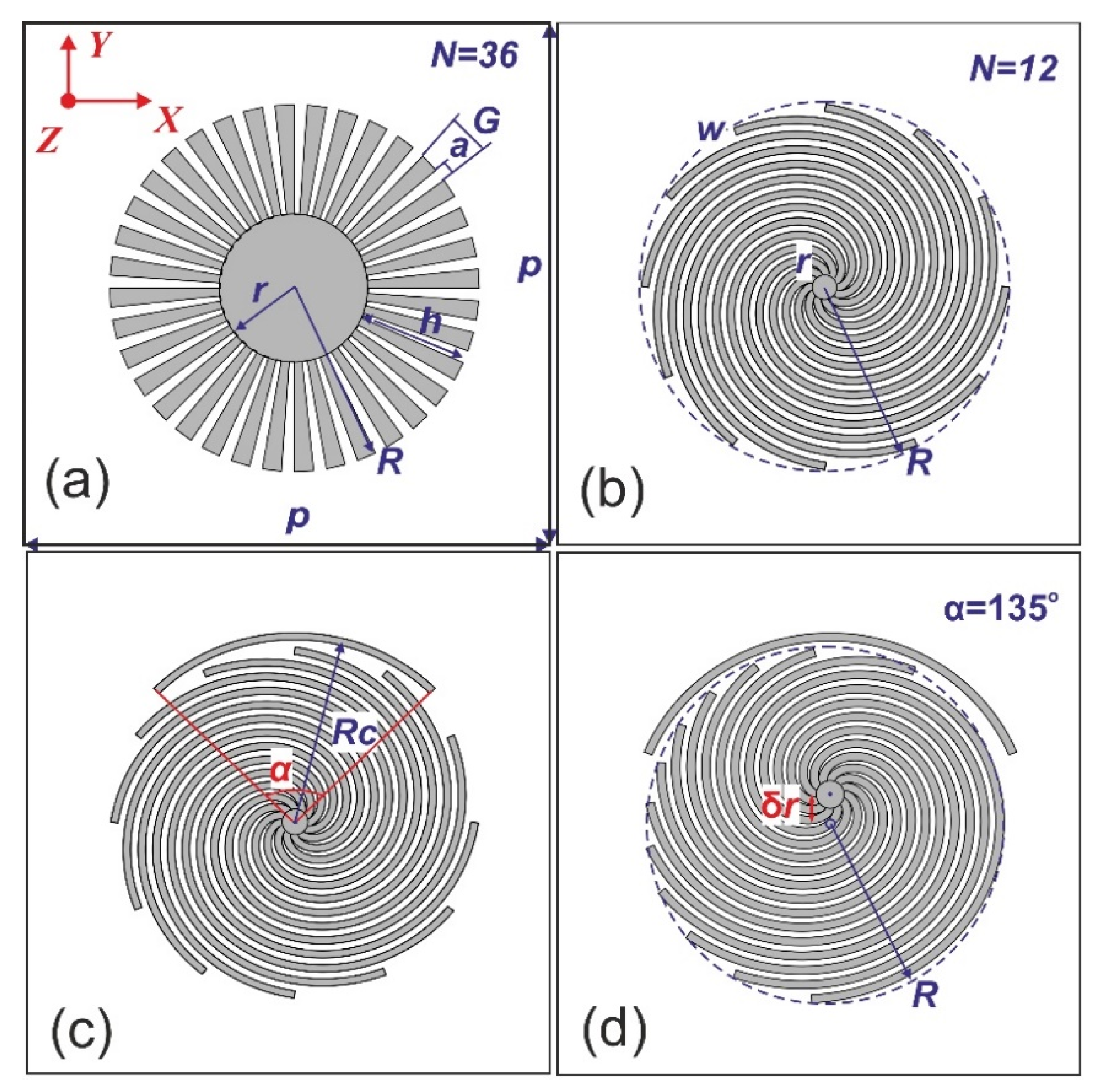
Abstract
:Featured Application
Abstract
1. Introduction
2. Materials and Methods
3. Results and Discussion
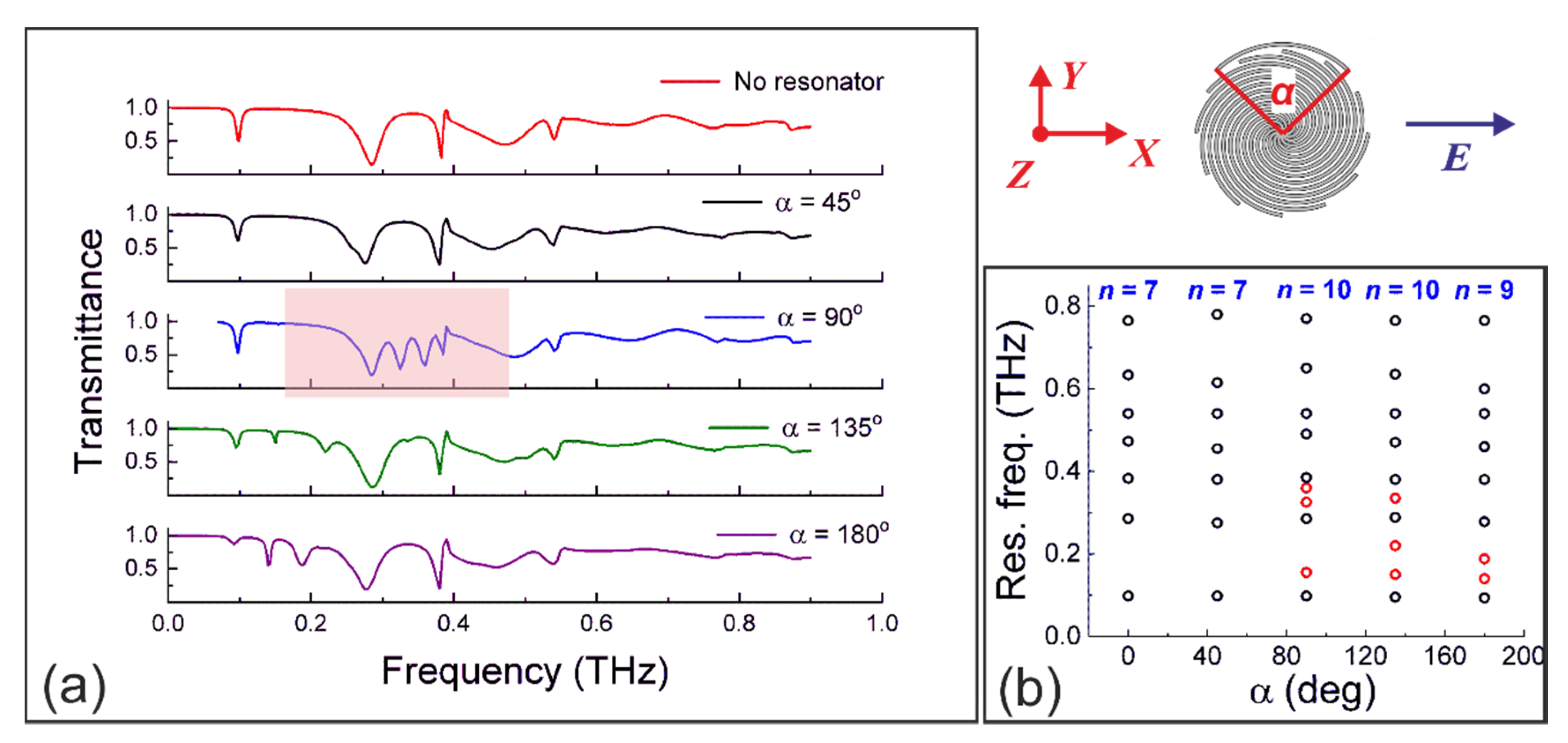
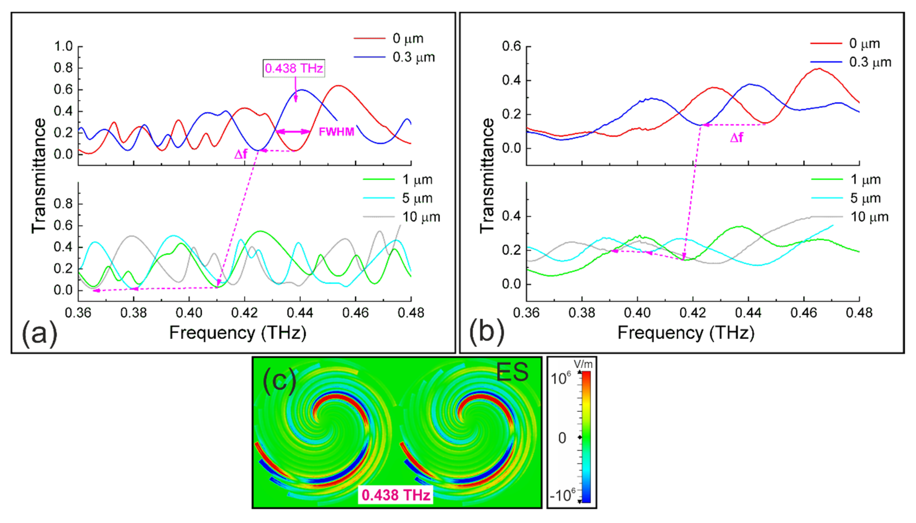
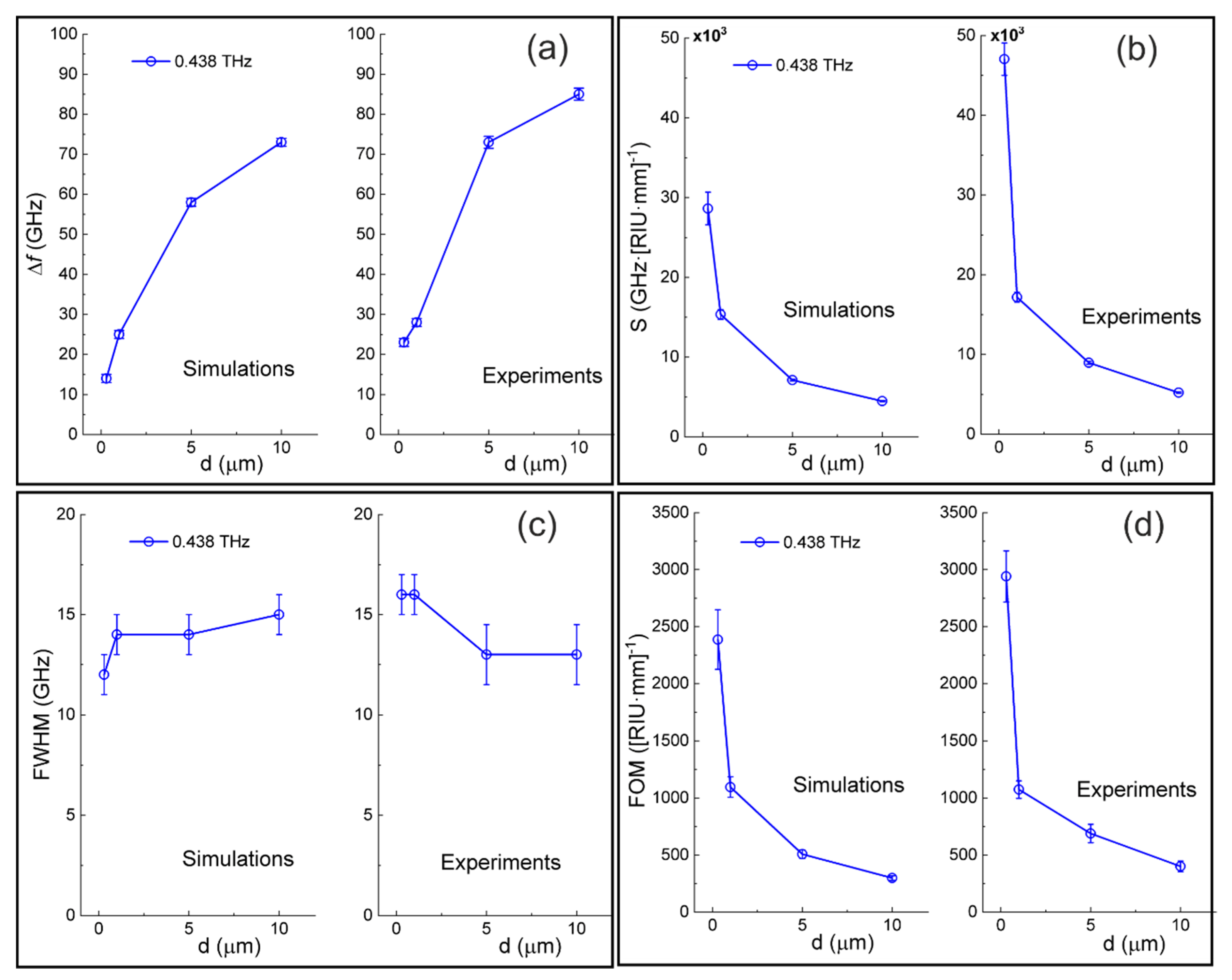
3.1. Symmetric Spiral Disks
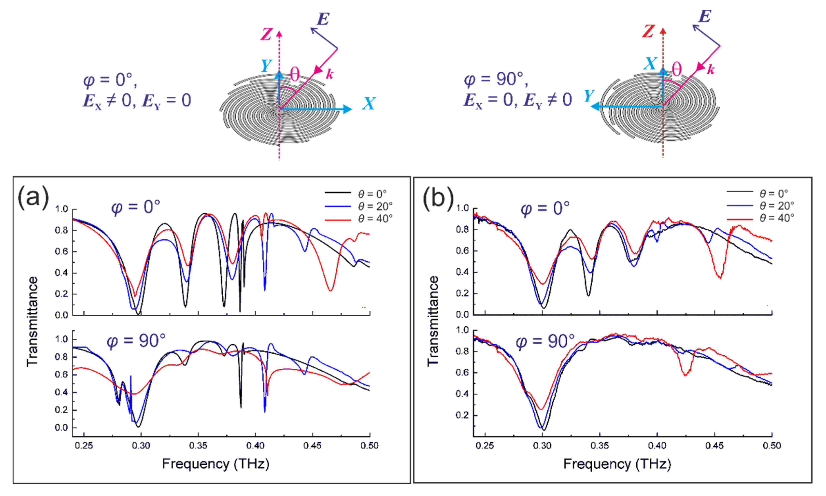
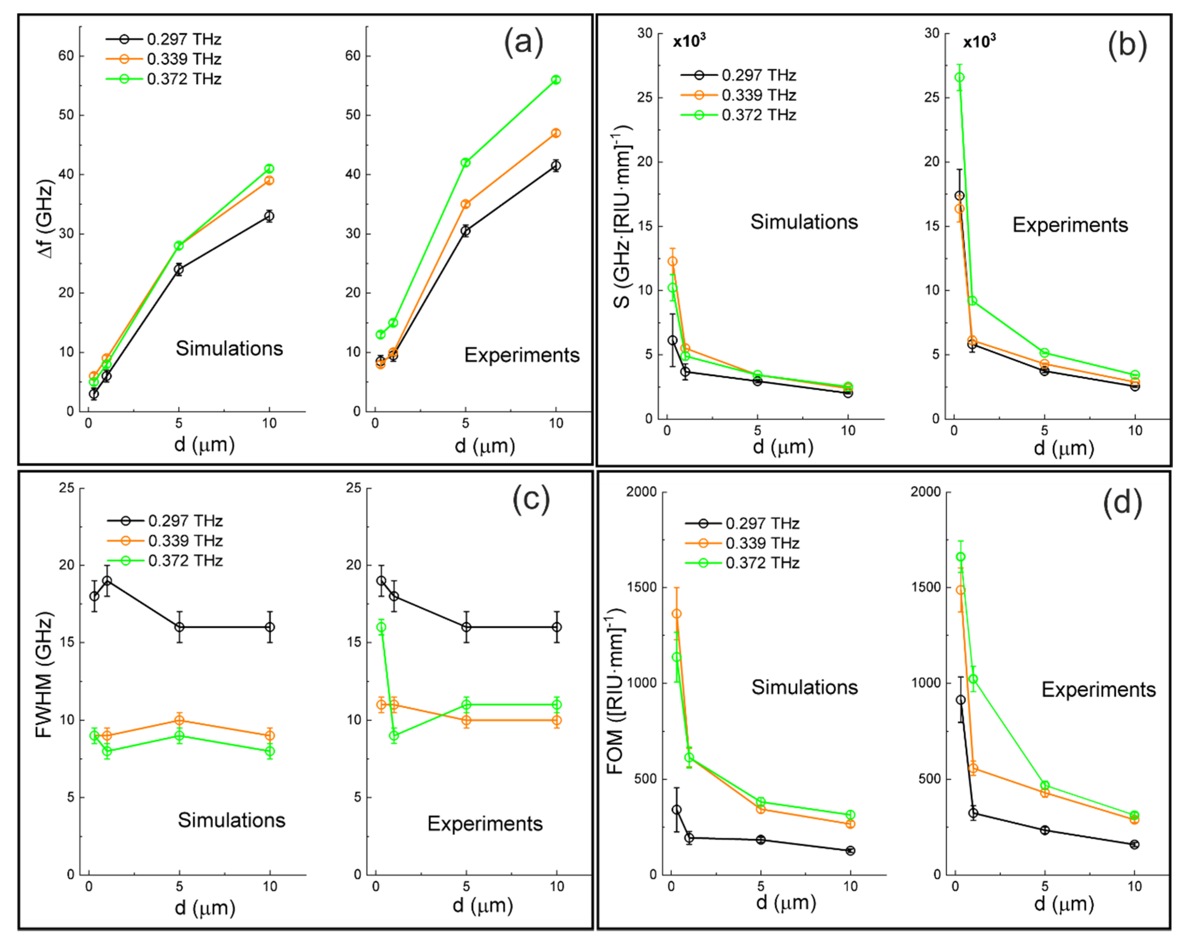
3.2. Asymmetric Spiral Disks with Shifted Center
4. Conclusions
Author Contributions
Funding
Acknowledgments
Conflicts of Interest
References
- Maier, S.A. Plasmonics: Fundamentals and Applications; Springer: New York, NY, USA, 2007. [Google Scholar]
- Anker, J.N.; Hall, W.P.; Lyandres, O.; Shah, N.C.; Zhao, J.; Van Duyne, R.P. Biosensing with plasmonic nanosensors. Nat. Mater. 2008, 7, 442–453. [Google Scholar] [CrossRef]
- Stiles, P.L.; Dieringer, J.A.; Shah, N.C.; Van Duyne, R.P. Surface-enhanced Raman spectroscopy. Annu. Rev. Anal. Chem. 2008, 1, 601–626. [Google Scholar] [CrossRef] [PubMed] [Green Version]
- Lakowicz, J.R.; Ray, K.; Chowdhury, M.; Szmacinski, H.; Fu, Y.; Zhang, J.; Nowaczyk, K. Plasmon-controlled fluorescence: A new paradigm in fluorescence spectroscopy. Analyst 2008, 133, 1308–1346. [Google Scholar] [CrossRef] [PubMed] [Green Version]
- Valev, V.K.; Silhanek, A.V.; Verellen, N.; Gillijns, W.; Van Dorpe, P.; Aktsipetrov, O.A.; Vandenbosch, G.A.; Moshchalkov, V.V.; Verbiest, T. Asymmetric optical second-harmonic generation from chiral G-shaped gold nanostructures. Phys. Rev. Lett. 2010, 104, 127401. [Google Scholar] [CrossRef] [PubMed] [Green Version]
- Atwater, H.A.; Polman, A. Plasmonics for improved photovoltaic devices. Nat. Mater. 2010, 9, 205–213. [Google Scholar] [CrossRef] [PubMed]
- Tian, Y.; Tatsuma, T.J. Mechanisms and applications of plasmon-induced charge separation at TiO2 films loaded with gold nanoparticles. J. Am. Chem. Soc. 2005, 127, 7632–7637. [Google Scholar] [CrossRef] [PubMed]
- Son, J.H. (Ed.) Terahertz Biomedical Science and Technology; CRC Press: Boca Raton, FL, USA, 2014. [Google Scholar]
- Peiponen, K.E.; Zeitler, J.A.; Kuwata-Gonokami, M. (Eds.) Terahertz Spectroscopy and Imaging. Springer Series in Optical Sciences; Springer: Berlin/Heidelberg, Germany, 2013; Volume 171. [Google Scholar]
- Lee, Y.-S. Principles of Terahertz Science and Technology; Springer: New York, NY, USA, 2009. [Google Scholar]
- Ordal, M.A.; Bell, R.J.; Alexander, R.W.; Long, L.L.; Querry, M.R. Optical properties of fourteen metals in the infrared and far infrared: Al, Co, Cu, Au, Fe, Pb, Ni, Pd, Pt, Ag, Ti, and W. Appl. Opt. 1985, 24, 4493–4499. [Google Scholar] [CrossRef]
- Pendry, J.B.; Martin-Moreno, L.; Garcia-Vidal, F.J. Mimicking surface plasmons with structured surfaces. Science 2004, 305, 847–848. [Google Scholar] [CrossRef]
- Pors, A.; Moreno, E.; Martin-Moreno, L.; Pendry, J.B.; Garcia-Vidal, F. Localized spoof plasmons arise while texturing closed surfaces. Phys. Rev. Lett. 2012, 108, 223905. [Google Scholar] [CrossRef] [Green Version]
- Glybovski, S.B.; Tretyakov, S.A.; Belov, P.A.; Kivshar, Y.S.; Simovski, C.R. Metasurfaces: From microwaves to visible. Phys. Rep. 2016, 634, 1–72. [Google Scholar]
- Al-Naib, I.; Withayachumnankul, W. Recent progress in terahertz metasurfaces. J. Infrared Millim. Terahertz Waves 2017, 38, 1067–1084. [Google Scholar] [CrossRef]
- Beruete, M.; Jáuregui-López, I. Terahertz sensing based on metasurfaces. Adv. Opt. Mater. 2020, 8, 1900721. [Google Scholar] [CrossRef] [Green Version]
- Liao, Z.; Shen, X.; Pan, B.C.; Zhao, J.; Luo, Y.; Cui, T.J. Combined system for efficient excitation and capture of LSP resonances and flexible control of SPP transmissions. ACS Photonics 2015, 2, 738–743. [Google Scholar] [CrossRef]
- Chen, L.; Wei, Y.M.; Zang, X.F.; Zhu, Y.M.; Zhuang, S.L. Excitation of dark multipolar plasmonic resonances at terahertz frequencies. Sci. Rep. 2016, 6, 22027. [Google Scholar] [CrossRef] [PubMed]
- Bulgakova, V.; Gerasimov, V.; Lemzyakov, A.; Milekhin, I.A. Infrared localized surface plasmon resonances on subwavelength corrugated metal disks. In Proceedings of the 43th International Conference IRMMW-THz, Nagoya, Japan, 9–14 September 2018. [Google Scholar]
- Gerasimov, V.V.; Kuznetsov, S.A.; Lemzyakov, A.G.; Hafizov, R.R. Multipole terahertz localized plasmon resonances on spiral structures. In Proceedings of the 44th International Conference IRMMW-THz, Paris, France, 1–6 September 2019. [Google Scholar]
- Huidobro, P.A.; Shen, X.; Cuerda, J.; Moreno, E.; Martin-Moreno, L.; Garcia-Vidal, F.J.; Cui, T.J.; Pendry, J.B. Magnetic localized surface plasmons. Phys. Rev. X 2014, 4, 021003. [Google Scholar]
- Gao, Z.; Wu, L.; Gao, F.; Luo, Y.; Zhang, B. Spoof Plasmonics: From metamaterial concept to topological description. Adv. Mater. 2018, 30, 1706683. [Google Scholar] [CrossRef]
- Liao, Z.; Fernández-Domínguez, A.I.; Zhang, J.; Maier, S.A.; Cui, T.J.; Luo, Y. Homogenous metamaterial description of localized spoof plasmons in spiral geometries. ACS Photonics 2016, 3, 1768–1775. [Google Scholar]
- Liao, Z.; Liu, S.; Ma, H.F.; Li, C.; Cui, J.; Cui, T.J. Electromagnetically induced transparency metamaterial based on spoof localized surface plasmons at terahertz frequencies. Sci. Rep. 2016, 6, 27596. [Google Scholar] [CrossRef] [Green Version]
- Kuznetsov, S.A.; Paulish, A.G.; Navarro-Cía, M.; Arzhannikov, A.V. Selective pyroelectric detection of millimetre waves using ultra-thin metasurface absorbers. Sci. Rep. 2016, 6, 21079. [Google Scholar] [CrossRef] [Green Version]
- Navarro-Cia, M.; Kuznetsov, S.A.; Aznabet, M.; Beruete, M.; Falcone, F.; Ayza, M.S. Route for bulk millimeter wave and terahertz metamaterial design. IEEE J. Quantum. Electron. 2011, 47, 375–385. [Google Scholar] [CrossRef]
- Aznabet, M.; Navarro-Cía, M.; Kuznetsov, S.A.; Gelfand, A.V.; Fedorinina, N.I.; Goncharov, Y.G.; Beruete, M.; El Mrabet, O.; Sorolla, M. Polypropylene-substrate-based SRR- And CSRR-metasurfaces for submillimeter waves. Opt. Express 2008, 16, 18312–18319. [Google Scholar] [CrossRef] [Green Version]
- Kuznetsov, S.A.; Arzhannikov, A.V.; Kubarev, V.V.; Kalinin, P.V.; Sorolla, M.; Navarro-Cía, M.; Aznabet, M.; Beruete, M.; Falcone, F.; Goncharov, Y.G.; et al. Development and characterization of quasi-optical mesh filters and metastructures for subterahertz and terahertz applications. Key Eng. Mater. 2010, 437, 276–280. [Google Scholar] [CrossRef]
- ALLRESIST GmbH. Available online: https://www.allresist.com (accessed on 21 May 2020).
- Jauregui-López, I.; Rodriguez-Ulibarri, P.; Kuznetsov, S.A.; Nikolaev, N.A.; Beruete, M. THz sensing with anomalous extraordinary optical transmission hole arrays. Sensors 2018, 18, 3848. [Google Scholar] [CrossRef] [Green Version]
- Kozlov, G.; Volkov, A. Coherent source submillimeter wave spectroscopy. In Millimeter and Submillimeter Wave Spectroscopy of Solids. Topics in Applied Physics; Grüner, G., Ed.; Springer: Berlin/Heidelberg, Germany, 1998; Volume 74, pp. 51–109. [Google Scholar]
- Sayanskiy, A.; Kuznetsov, S.A.; Tanygina, D.S.; Risco, J.P.; Glybovski, S.; Baena, J.D. Frequency controllable polarization rotation of THz waves with an SCMS. IEEE Trans. Antennas Propag. 2019, 68, 1491–1502. [Google Scholar] [CrossRef]
- Kuznetsov, S.A.; Paulish, A.G.; Gelfand, A.V.; Lazorskiy, P.A.; Fedorinin, V.N. Bolometric THz-to-IR converter for terahertz imaging. Appl. Phys. Lett. 2011, 99, 023501. [Google Scholar] [CrossRef]
- Rodríguez-Ulibarri, P.; Kuznetsov, S.A.; Beruete, M. Wide angle terahertz sensing with a cross-dipole frequency selective surface. Appl. Phys. Lett. 2016, 108, 111104. [Google Scholar] [CrossRef]
- Jáuregui-López, I.; Rodríguez-Ulibarri, P.; Urrutia, A.; Kuznetsov, S.A.; Beruete, M. Labyrinth metasurface absorber for ultra-high-sensitivity terahertz thin film sensing. Phys. Status Solidi 2018, 12, 1800375. [Google Scholar] [CrossRef]
- Zhang, J.; Liao, Z.; Luo, Y.; Shen, X.; Maier, S.A.; Cui, T.J. Spoof plasmon hybridization. Laser Photonics 2017, 11, 1600191. [Google Scholar] [CrossRef] [Green Version]
- Koshelev, K.; Lepeshov, S.; Liu, M.; Bogdanov, A.; Kivshar, Y. Asymmetric metasurfaces with high-Q resonances governed by bound states in the continuum. Phys. Rev. Lett. 2018, 121, 193903. [Google Scholar] [CrossRef] [Green Version]


© 2020 by the authors. Licensee MDPI, Basel, Switzerland. This article is an open access article distributed under the terms and conditions of the Creative Commons Attribution (CC BY) license (http://creativecommons.org/licenses/by/4.0/).
Share and Cite
Gerasimov, V.V.; Hafizov, R.R.; Kuznetsov, S.A.; Lazorskiy, P.A. Exploiting Localized Surface Plasmon Resonances in Subwavelength Spiral Disks for THz Thin Film Sensing. Appl. Sci. 2020, 10, 3595. https://0-doi-org.brum.beds.ac.uk/10.3390/app10103595
Gerasimov VV, Hafizov RR, Kuznetsov SA, Lazorskiy PA. Exploiting Localized Surface Plasmon Resonances in Subwavelength Spiral Disks for THz Thin Film Sensing. Applied Sciences. 2020; 10(10):3595. https://0-doi-org.brum.beds.ac.uk/10.3390/app10103595
Chicago/Turabian StyleGerasimov, Vasily V., Ruslan R. Hafizov, Sergei A. Kuznetsov, and Pavel A. Lazorskiy. 2020. "Exploiting Localized Surface Plasmon Resonances in Subwavelength Spiral Disks for THz Thin Film Sensing" Applied Sciences 10, no. 10: 3595. https://0-doi-org.brum.beds.ac.uk/10.3390/app10103595