Power Loss Analysis and a Control Strategy of an Active Cell Balancing System Based on a Bidirectional Flyback Converter


1
Department of Electrical Engineering, National Taiwan University of Science & Technology, Taipei 106, Taiwan
2
Department of Information and Communication Engineering, St. John’s University, Taipei 499, Taiwan
*
Author to whom correspondence should be addressed.
Appl. Sci. 2020, 10(12), 4380; https://0-doi-org.brum.beds.ac.uk/10.3390/app10124380
Submission received: 2 June 2020
/
Revised: 19 June 2020
/
Accepted: 22 June 2020
/
Published: 25 June 2020
(This article belongs to the Special Issue Resonant Converter in Power Electronics Technology)
Abstract
:Featured Application
Battery Management System.
Abstract
This research proposes a power loss analysis and a control strategy of an active cell balancing system based on a bidirectional flyback converter. The system aims to achieve an energy storage application with cells connected in 6 series and 1 parrarel (6S1P) design. To reduce the structural complexity, Metal-Oxide-Semiconductor Field Effect Transistor (MOSFET) array commonly used in balancing system is replaced with the photovoltaic Metal-Oxide-Semiconductor (photoMOS) array. Power loss analysis is utilized for the system operating in the proper current to reach higher efficiency. The proposed loss models are divided into conduction loss, switching loss, and copper and core loss of the transformer. Besides, the models are used to estimate the loss of converter operating in different balance conditions to evaluate the system efficiency and verified by the implemented balancing circuit. By way of the loss models, the balancing current can be determined to reach higher efficiency of the proposed system. For further improvement of the balancing process, the system has also applied a control strategy to enhance the balancing performance that reduces 50% maximum voltage difference than traditional cell-to-pack architecture, and 47% balancing duration than traditional pack-to-cell architecture.
1. Introduction
In recent years, with the development of science and technology, the issue of energy shortages in island countries and outlying islands has been expanding. Based on energy shortage and environmental awareness, a microgrid with an energy storage system (ESS) has become one of the main projects for the development of science and technology [1]. Usually, ESS utilizes battery modules as energy storage devices, but the battery modules are not only expensive but also account for a relatively high proportion of the overall cost of ESS. Therefore, it is even more important to extend battery life. Battery modules are usually composed of cells in series and parallel. However, even the same batch of cells produced from the same manufactory have different characteristics from each other. These differences will become more apparent over time and reduce the life and safety of battery modules. To figure out this problem, it is essential to develop the technology of the battery management system (BMS). The BMS technology can increase the maximum capacity of the battery module and extend the life of the battery module. The principal function of BMS is to monitor, protect, and balance the battery module [2,3]. The BMS monitors various parameters such as voltage, current, and temperature of each cell in the battery module to ensure that the battery module works in a stable condition; the protection function provides over-voltage, under-voltage, over-current, over-temperature, and under-temperature prevention. Thus, appropriate protection ensures that the battery module operates safely and normally; the balancing function is mainly to improve the imbalance problem in the battery module due to the different characteristics of each cell. The balance circuit rearranges the energy among cells until the power of each cell reaches equilibrium to maximize the energy capacity and prolong the lifetime of the battery module.
So far, many researchers have proposed various kinds of balance circuit architectures [4,5,6,7,8,9,10,11,12]. Amin employed a passive balancing BMS that combines the power resistor and Metal-Oxide-Semiconductor Field Effect Transistor (MOSFET) internal resistance as a balancing resistor to save the space [4]. Antonio Manenti proposed a BMS architecture based on cell redundancy [5]. These two studies belong to passive balancing methods. Passive balancing methods have the least system cost but must take into account the heat issue. The balancing current is usually limited to less than 50 mA. If the current is set too large, the heat generated by the power consumed by the resistor may damage the battery module. On the other hand, if the current is low, the balancing time will significantly increase. Kyung-Min Lee introduced an inductance-capacitance (LC) series resonant circuit as an energy carrier, which transfers the balancing energy directly from the highest charged cell to the lowest charge cell [6]. However, the LC series resonant method needs to control the switches rapidly to achieve the balancing process. Ming Liu utilized megahertz multiple-receiver wireless power transfer to achieve battery cell equalization [7]. However, wireless power transfer has low efficiency and it is unable to control the balancing current for each cell. Federico Baronti described the design and safety verification of a novel charge equalizer with a fully distributed architecture, which not only perfectly fits the typical partitioning of a battery into modules, but also achieves the system with a simple circuit structure [8]. Whereas this cell equalizer cannot reach the adjustable balancing current. Federico Baronti also designed a high-efficiency digitally controlled charge equalizer for series-connected cells based on switching converter and super-capacitor [9]. This equalizer he proposed is similar to capacitive shuttle cell balancing, which has energy recycling and the system cost is still low but it still needs an amount of time to complete the balancing process.
Wangxin Huang presented an energy sharing state-of-charge (SOC) balancing control scheme based on a distributed BMS architecture where the dc bus voltage regulation system and the cell balancing system are combined into a single system [10]. Cells in the pack are separated by the converter, and the converters’ output is connected in series so that the system should apply current-sharing control to maintain the stability of the direct current (DC) bus. Mohammad Abdul Hannan achieved cell-balancing by a bidirectional flyback dc-dc converter [11]. The bidirectional flyback dc-dc converter proposed by the researcher is conposed of two traditional flyback dc-dc converters that each one takes charge of one power direction. It will cost more than using a bidirectional flyback dc-dc converter instead which is one of the most important elements in the solution adopted in this work. Sang-Won LEE raised a modularized design of active cell-to-cell/module-to-module charge equalizer [12]. Compared with the equalizer implemented by Kyung-Min Lee [6], the design has removed the capacitor of the LC circuit to further reduce the system cost. Nevertheless, the problem has to be solved that the design must deal with the inrush current when the two balancing batteries have a large voltage difference.
There are more active cell balancing systems which have not been mentioned above. According to the balancing patterns, active cell balancing systems can be divided into three categories: capacitive shuttle cell balancing [13,14,15,16], inductive shuttle cell balancing [12,17,18,19,20,21], and individual charging cell balancing [6,9,22,23,24,25,26]. The capacitor shuttle system has less loss, but it takes a longer time to complete the balancing process. The inductance shuttle system also has a low loss. Nevertheless, the cost is more than the capacitor shuttle method because of its complicated switch structure. The individual charging system works the most efficiently but at a greater expense.
However, most of the capacitive shuttle system and the inductive shuttle system can only transfer energy to adjacent cells, which will increase the time required to reach equilibrium in the battery module and reduce the efficiency of energy transfer. In contrast, the individual charging system performs more effectively than the other. It can reduce the balance time and increase the efficiency of energy transfer. The individual charging system has the following forms: buck-boost converter, quasi-resonant buck-boost converter, and flyback converter. Each type of individual method benefits from its structure, such as balancing duration, balancing times, the complexity of architecture, or cost. Taking all the factors into consideration, this research implements an active cell balancing circuit based on a bidirectional flyback converter. The proposed system further improves the system by applying a control strategy which is able to reduce the balancing duration. Moreover, this research also proposes loss models to estimate the bidirectional flyback converter to discuss how to determine the proper balancing current of the proposed circuit to achieve the highest efficiency of the bidirectional flyback converter and reduce the losses in the balancing process.
2. Hardware Description of the Proposed Cell Balancing System
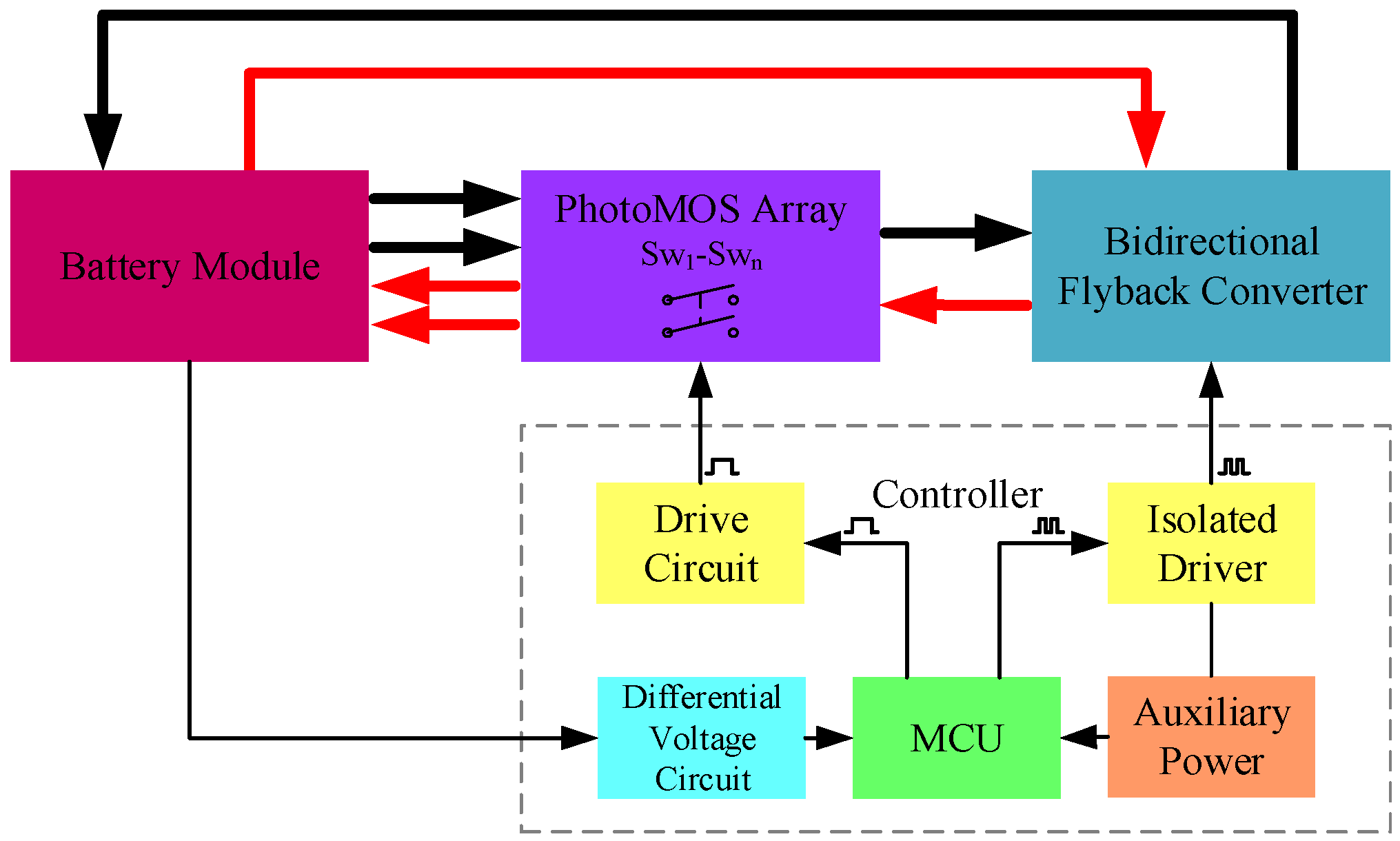
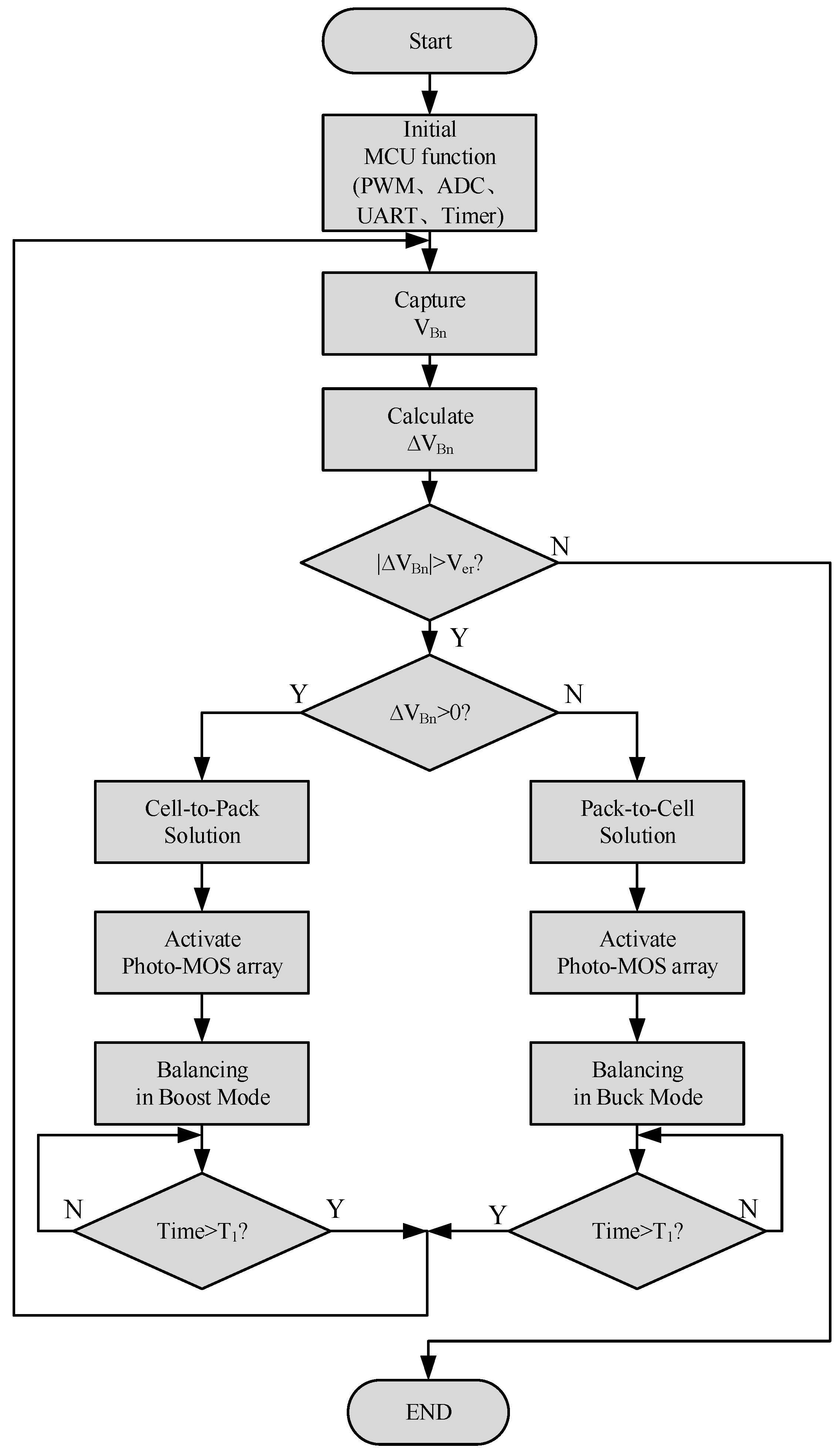
In this research, the proposed system is developed for a cells connected in 6 series and 1 parrarel (6S1P) battery pack. The reason why the system is only for a small pack is that it can be series-connected to reach a higher voltages, such as 48 V or 400 V. The specification can be obtained in Section 4. Figure 1 shows the block diagram of the proposed cell balancing system, which consists of a bidirectional flyback converter, a microcontroller unit (MCU:dsPIC33FJ64GS606) manufactured by Microchip Technology in Chandler, Arizona, United States, a photoMOS array, an auxiliary power circuit, a differential voltage circuit, and driver circuits. In this research, the bidirectional flyback is the key part of the system, which can realize energy transfer in both directions, to achieve the balancing function with a simpler structure. The microcontroller unit (MCU) shown in Figure 1 not only provides the control signal for the photoMOS and bidirectional flyback converter but also receives all the voltage of cells by the differential voltage circuit, then applies the control strategy via the signal captured to complete the balancing process more efficiently. Its control strategy can be observed in Figure 2, where VBn is the voltage of each cell, ∆VBn is the voltage difference between each cell and the average voltage of all the cells, Ver is the parameter of the minimum voltage error to activate the balancing process, and T1 is the time duration for a single balancing process. The MCU will gather the voltages of the cells through a differential voltage circuit. By calculating the ∆VBn of each cell, the system will decide which cell needs to be balanced. If the chosen cell has the highest voltage, the cell-to-pack solution will be carried out, and the balancing system will be operated in boost mode until the timer counts up to T1. If the chosen cell has the lowest voltage, the pack-to-cell solution will be carried out, and the balancing system will be operated in buck mode until the timer counts up to T1.
The common individual charge battery balance architecture can only realize energy transfer in one direction. For example, the pack-to-cell architecture has the ability to effectively charge the cell which capacity is low, but it cannot efficiently transfer the energy of the cell which capacity is high to the pack; the cell-to-pack architecture is able to transfer the energy from the cell which has a higher capacity to the pack effectually, but it is unable to charge the low capacity cell with the pack very efficaciously. The implemented cell balancing system has the most important feature that the energy can be extracted not only from pack to cell but also from cell to pack. To achieve the bidirectional balancing behavior, the implemented system replaces the rectifier diode in the traditional flyback converter with synchronous rectification MOSFET and simultaneously reduces the losses caused by the output rectifier diode. Compared with the system using a multi-winding transformer or multiple flyback converters [26], it simplifies the structure by applying a bidirectional flyback converter with a switch array instead and reduces the cost further by replacing MOSFET with photoMOS in the switch array. Furthermore, the commonly used converter in balancing systems operates with a low constant current, while the proposed solution can implement an adjustable balancing current not only for various control strategies, but also for efficiency measurement of the system operating in different curents.
3. Power Loss Analysis of the Cell Balancing System
The proposed cell balancing system, as shown in Figure 3, is realized through the bidirectional flyback converter topology where VBn is the voltage of nth cell, Sn is the photoMOS array, Lm is the field inductor of the transformer, N is the turn ratio of the transformer, and Q1 and Q2 are the MOSFET for switching. The designed cell balancing system utilizes a 6S1P lithium ternary battery module. The cells’ state of charge will determine the operation mode of the photoMOS relay and the MOSFETs. Figure 4 shows that the proposed has two operation modes, where I1 is the balancing current, and I2 is the current at high side. Mode A is a boost mode. For example, when the voltage VB1 of the first cell is higher than the voltage of other cells in the module, the photoMOS S1 will be turned on, and the MOSFET Q1 will work as the main switch to control the circuit. The field inductor Lm of the transformer will store the energy of the cell, and transfer it to the battery module. The MOSFET Q2 will be operated with synchronous rectification control to reduce the conduction loss of the rectifier diode, as shown in Figure 4a; When the voltage VB1 of the first cell is less than the voltage of other cells in the module, the proposed system will operate in mode B. The photoMOS S1 will turn on, and the MOSFET Q2 will work as the main switch to control the circuit. The field inductor Lm of the transformer will store the energy of the battery module, and then transfer it to the cell. At this time, the MOSFET Q1 will be operated with synchronous rectification control to reduce the conduction loss of the rectifier diode, as shown in Figure 4b. By operating in these two modes alternately, after multiple balancing actions, the balancing system can achieve the equilibrium of the battery module.
To determine the best balance current to achieve the highest efficiency and the least losses of the proposed system, it is necessary to estimate the losses caused by each component of the balancing architecture during the energy transfer. In the cell balancing situation, to implement the bidirectional flyback converter, the designed converter will only operate in continuous conduction mode (CCM) to prevent the energy inversion. Therefore, all the losses are considered in CCM. The losses caused by gate drivers, differential voltage sensors, or photoMOS relays will not be taken into account either because the power loss analysis proposed by this research attempts to find the relation between operating current and the bidirectional flyback converter’s efficiency. In this case, the auxiliary power of those components is supplied by DC power manufactured by Gwinstek Company. The losses are mainly composed of the conduction and switching losses of the power switch, the copper and iron loss of the transformer, and the line loss. This research discusses the loss model of the proposed circuit operating in buck mode. As shown in Figure 5, this loss model replaces the battery module with the ideal voltage source Vpack. The cell is replaced by the ideal voltage source VBn. Rs is the wire resistance, RL is the resistance of the transformer, Rds1(on) is the on-resistance of MOSFET Q1, Rds2(on) is the on-resistance of MOSFET Q2, and Lm is the field inductor of the transformer. The main voltage and current waveforms of the bidirectional flyback converter operating in buck mode can be obtained in Figure 6, where vgs1 is the MOSFET Q1 gate signal, vgs2 is the MOSFET Q2 gate signal, vds1 is the voltage across the MOSFET Q1 from drain to source, vds2 is the voltage across the MOSFET Q2 from drain to source, iL is the current passing through the Lm, and iD is the current flowing through the MOSFET Q2.
First, the switching loss is loss caused by the current-voltage overlap region during the switching. Because this loss is very difficult to calculate accurately, this research uses the estimation method in the analysis of the MOSFET switching loss proposed by Z. John Shen to switch loss estimation [27], as shown in Figure 7 and Equation (1)
where IDS is the current on the MOSFET when turning on, VDS is the voltage across the drain-source of the MOSFET, ton and toff are the time required for the MOSFET to switch on and off, fsw is the frequency of the MOSFET operation, and Coss is the parasitic capacitor of the MOSFET. In buck mode, due to the synchronous rectification technology in the bidirectional flyback converter, only the MOSFET Q1 will generate switching losses.
Secondly, the conduction loss is caused by the energy transferring through the transformer, the wire resistance, and the switch’s on-resistance. The followings are two operating modes in a cycle. Utilizing the switching of MOSFET Q1 and Q2, these two modes will estimate the conduction loss caused by the energy transfer, as shown in Figure 6.
Interval I [t0–t1]:
In Interval I, the MOSFET Q1 is on, and the field inductor Lm of the transformer stores energy from battery module Vpack via the current iL. Since the current iL rises linearly, in the loss calculation in this mode, the current iL is averaged. As shown in Figure 5a, the current will pass through the wire resistance Rs and the on-resistance Rds1(on) of the MOSFET Q1. The loss formula is given in Equations (2) and (3)
when t = t1, the MOSFET Q1 turns off, and the MOSFET Q2 turns on. This mode ends.
Interval II [t1–t2]:
In Interval II, the MOSFET Q2 is on, and the field inductor Lm of the transformer charges the cell VBn via the current iL. Since the current iL decreases linearly, in the loss calculation in this mode, the current iL is averaged. As shown in Figure 5b, the current will pass through the on-resistance Rds2(on) of the MOSFET Q2. The loss formula is given in Equation (4).
when t = t2, the MOSFET Q2 turns off, and the MOSFET Q1 turns on. This mode ends.
Through the analysis above, the conduction loss in a cycle can be calculated as follows:
Besides, the loss of the transformer is divided into the copper loss (Pcopper) and the iron loss (Pcore). The copper loss is mainly caused by the current passing through the AC impedance RL(AC) of the transformer. However, RL(AC) is hard to estimate with a simple mathematical model because it is affected by the skin effect and the proximity effect. Moreover, these two effects are also influenced by the thickness, stacking, and coupling coefficient of the wire. While the transformer DC impedance RL(DC) is relatively easy to measure, to simplify the calculation of RL(AC), using the transformer AC impedance factor λ represents the relationship between RL(AC) and RL(DC) [28], as shown in Equation (10), and the copper loss is calculated as in Equation (11). The transformer iron loss calculation needs to query the corresponding transformer material, frequency, temperature, excitation current, etc. In the research, it is hard to obtain relevant parameters of the transformer used in the system, so the research takes the material of PC40 as an example, the iron loss formula provided by the manufacturer is as Equation (12) shown where △B is the magnetic induction intensity variation of the transformer, and the Ve is the effective volume of the transformer core.
The total loss of the system in a cycle can be obtained by summing up all the losses parts estimated above as
The loss model of the proposed circuit operating in boost mode is similar to the proposed operating in buck mode. The only difference is the current direction and parameters. Therefore, the loss model of the proposed circuit operating in boost mode will not be discussed in this research.
4. Design Considerations
The key parameters of the bidirectional flyback converter in the proposed cell balancing system are listed in Table 1, where the lithium-ion battery module has a 6S1P configuration with a rated capacity of 2500 mAH and a voltage range of 2.5 V–4.2 V for each cell. To achieve the desired bidirectional flyback converter with adjustable current, some component values should be selected or determined, such as operating voltage, balancing current which refers to the current I1 of the low side and is limited by the specification of the phototMOS (40 V, 2.5 A) for the safety, operating frequency, and duty cycle. The related design considerations are described below.
(1) Determine the turn ratio N of the transformer
The proposed system considers that it has a worse case in boost mode than in buck mode. According to the high-side voltage and low-side voltage, the turn ratio N from high side to low side will be designed in the worst case for operating in boost mode when high-side voltage Vpack(max) is 25.2 V and low-side Voltage VBn(max) is 2.5 V. Therefore, in the case of the maximum duty cycle DLmax of the boost mode as 0.8, we can calculate the turn ratio as
The turn ratio N as 0.396 means if the low side has one turn, the high side will have about 2.5 turns. In the practical design, the turn ratio N will be selected as 0.333 to make the high side have more turns to overcome the worse case and convenient for implementation.
(2) Determine the inductance of the field inductor in the transformer
The designed bidirectional converter set the crossing power Pcritical between DCM and CCM in the condition as 20% load. The equation is shown as
where β represents the ratio of the power Pcritical to maximum low-side power PBn(max), the low-side maximum voltage VBn(max) is 4.2 V, the maximum balancing current I1(max) is 2 A, the high-side minimum voltage Vpack(min) is 15 V, the maximum duty cycle DHmax of the buck mode is 0.45, and the operation frequency is 100 kHz. The actual inductance of the implemented field inductor of the transformer is 111.7 μH.
5. Experimental Verification
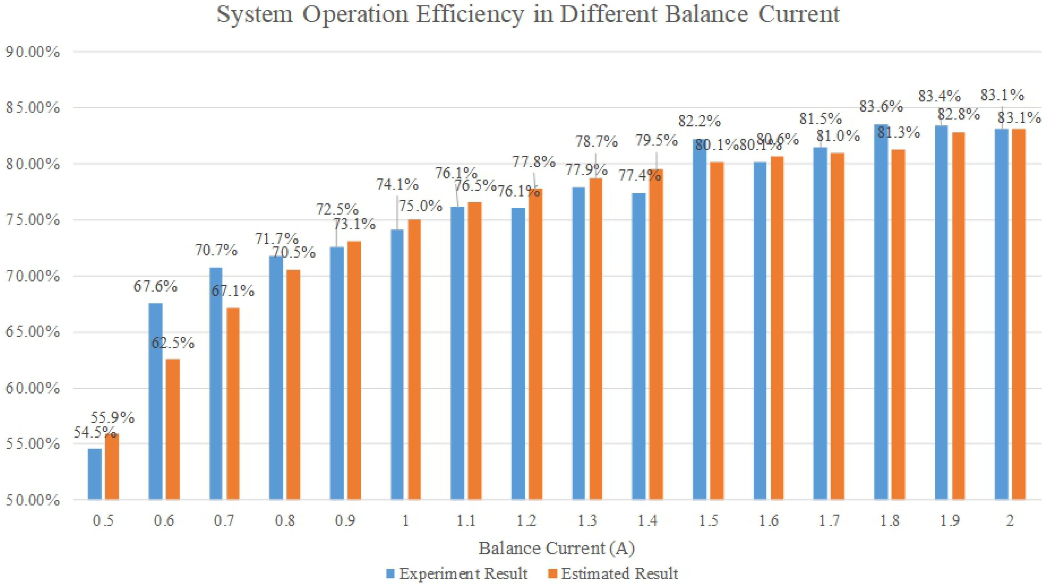
As shown in Figure 8, the photo of the implemented cell balancing system is used to verify the loss model proposed in this study through the test results. This research measures the efficiency of the bidirectional flyback converter by adjusting the operating current. The type of cell used in this study is the lithium ternary cell UR18650NSX produced by Panasonic, with a rated capacity of 2500 mAH and a voltage range of 2.5 V–4.2 V. Through the test of the 6S1P battery module, which is composed of the series connection of these kinds of cells, the voltage Vpack range at high side is 15 V~25.2 V, and the voltage VBn range at low side is 2.5 V–4.2 V. In the experiment, the efficiency test is carried out under the condition that the voltage Vpack is 20.9V and the voltage VBn is 4.2 V at the low side. The balance current I1 changes from 0.5 A to 2.0 A to observe the variety of efficiency. 0 shows the parameters and specifications of the model, where the model of MOSFET Q1 and Q2 is CSD18510KCS manufactured by TI company. It is worth mentioning that the parameter Rds(on) of MOSFET will change in different situations. In this research, the temperature of MOSFETs does not change much because the converter’s power is just about 8.4. W and the losses caused by MOSFETs is only about 0.05 W which will not increase the temperature of MOSFETs during operation. According to the datasheet of CSD18510KCS, this research estimates Rds(on) as 1.4 mΩ based on MOSFETs’ temperature as 25 °C and vgs as 15 V. The balancing system is implemented by utilizing TLP250H as gate drivers, LM358 as operational amplifier to achieve the voltage sensing, and LT318 as photoMOS relays. The loss analysis formula is shown in Equations (7)–(13). The results are shown in Figure 9 and compared with the hardware measurement which using the DC Power (62100H-600S) and DC Load (63204A-600-280) manufactured by Chroma Company to acquire the system efficiency in the different operating currents. It can be obtained that the balance current of the designed bidirectional flyback converter is proportional to the operation efficiency under the test conditions shown in Table 2.
Figure 9 shows the hardware waveforms of the developed prototype operating in buck mode with Vpack as 15 V and balancing current I1 as 1 A and is aimed to verify the veracity of the system, where vgs1 is the gate signal voltage of MOSFET Q1, vgs2 is the gate signal voltage of MOSFET Q2, vds1 is the voltage across the MOSFET Q1 from drain to source, vds2 is the voltage across the MOSFET Q2 from drain to source, iL is the current passing through the Lm, and iD is the current flowing through the MOSFET Q2, and i1 is the current at low side output and regards as the balancing current. Then, the prediction and actual measurement results are processed by the mean absolute error (MAE). The formula is shown in Equation (18), where n is the number of comparisons, ηrea_i is the measured efficiency, and ηest_i is the estimated efficiency. In Figure 10, it can be observed that the maximum error is 5.06%, the minimum error is 0.02%, and the average absolute error is 1.48%.
The efficiency distribution of the proposed can be obtained in Figure 9. In the literature, there is hardly any discussion about the relationship between balancing current and operation efficiency. Therefore, this research still collects the efficiency of the system mentioned in Section 1. The comparison is shown in Table 3, although they are all operated in different situations. The capacitor shuttle system like Wangxin Huang’s design will have the highest efficiency, the system proposed by Ming Liu has a lower efficiency in his test condition, and the individual charging cell balancing systems in all the research mentioned own the system efficiency from 70% to 90%. Therefore, the purpose of the power loss analysis in this research is highly necessary to achieve higher efficiency in the system.
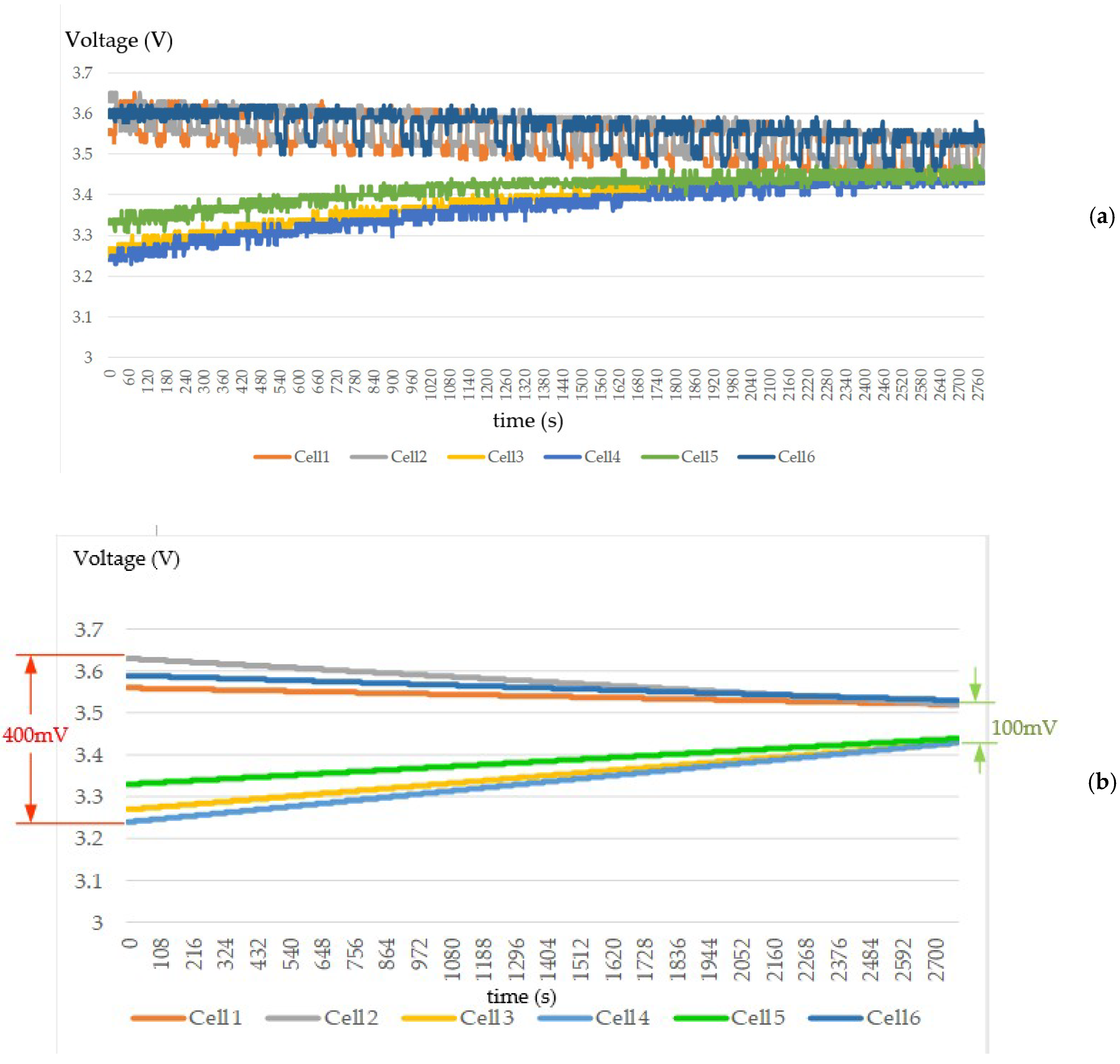
Another important purpose of this research is to improve the performance of the proposed cell balancing system by applying the control strategy. To verify the effect of the control strategy, the experiments will be conducted under the conditions shown in Table 4. During the testing, Ver will be set as 50 mV, I1 as 1 A, and T1 as 30 s. To compare among the pack-to-cell, the cell-to-pack, and the bidirectional architecture, the proposed cell balancing system will operate in three diverse control strategies. First of all, the system will complete the balancing process the same as the pack-to-cell architecture by only carrying out the pack-to-cell procedure. Secondly, the proposed system will merely operate with the cell-to-pack program to reach battery module equilibrium in a similar way as the cell-to-pack architecture. The last one, implemented in this research, is that the system combines the cell-to-pack and the pack-to-cell functions, including both of the advantages, to get the battery module balanced. The experimental results will be shown in Figure 11, Figure 12 and Figure 13, where Figure 11a, Figure 12a and Figure 13a are the actual hardware measurements of each cell’s voltage by the differential voltage circuit shown in Figure 1 for three different balancing processes. To obtain the trend of the voltage varieties in the battery module, Figure 11b, Figure 12b and Figure 13b show the processed results for the significant changes.
After the collation of the data shown above, this research gives a table, as shown in Table 5, to compare the balancing duration and maximum error among three balancing processes. The maximum voltage error is the voltage difference between the cell with the highest voltage and the cell with the lowest voltage. The cell-to-pack control takes 2783 s to complete the balancing process with a 100 mV voltage difference left. The pack-to-cell control spends 5175 s to balance the battery module, but its maximum voltage error can not be reduced anymore at 130 mV. The bidirectional control has the least balancing duration as 2727 s and it is able to decrease the maximum voltage error to 50 mV. It can be obtained that the implemented bidirectional control strategy, which will always balance the cell having the most voltage difference to the average cell voltage Vavg in the battery module, has a less balancing duration than the pack-to-cell and a less maximum voltage error between the cell with the highest voltage and the one with the lowest voltage.
6. Conclusions
In this paper, a power loss analysis and a control strategy of an active balancing circuit based on a bidirectional flyback converter are proposed and evaluated. From the analysis of the experimental data, the maximum error between the loss model and the measured results is 5.06%, the minimum error is 0.02%, and the average absolute error is 1.48%. Moreover, the designed bidirectional flyback converter has the highest efficiency when the balancing current reaches 2 A, and it can also reduce the time required for completing the balancing process. Therefore, we can derive the most important parameter in the balancing process by the proposed power loss model according to the desired conditions, such as balancing speed or system efficiency. Finally, the system applies a bidirectional control strategy, compared with the cell-to-pack and the pack-to-cell control, which has a less balancing duration as 2727 s and a less maximum voltage error 50 mV in the case of the balancing current as 1 A, to improve the efficiency of the balancing process.
Author Contributions
Conceptualization, C.-H.L. and Y.-L.L.; Methodology, Y.-L.L.; Software, Y.-L.L. and S.-J.Y.; Validation, Y.-L.L. and S.-J.Y.; Formal analysis, Y.-L.L.; Investigation, C.-H.L.; Resources, C.-H.L.; Data curation, Y.-L.L.; Writing—original draft preparation, Y.-L.L.; Writing—review and editing, C.-H.L. and S.-J.Y.; Project administration, C.-H.L.; Funding acquisition, C.-H.L. All authors have read and agreed to the published version of the manuscript.
Funding
This research was funded by the Ministry of Science and Technology, Taiwan, R.O.C., grant number MOST 106-2221-E-011-094-MY3 and by the National Chung-Shan Institute of Science and Technology, grant number NCSIST-104-V409(107).
Acknowledgments
The authors sincerely appreciate much supports from the Taiwan Building Technology Center from The Featured Areas Research Center Program within the framework of the Higher Education Sprout Project by the Ministry of Education in Taiwan.
Conflicts of Interest
The authors declare no conflict of interest.
References
- Tran, D.; Khambadkone, A.M. Energy Management for Lifetime Extension of Energy Storage System in Micro-Grid Applications. IEEE Trans. Smart Grid 2013, 4, 1289–1296. [Google Scholar] [CrossRef]
- Chen, C.-L.; Wang, D.-S.; Li, J.-J.; Wang, C.C. A Voltage Monitoring IC with HV Multiplexer and HV Transceiver for Battery Management Systems. IEEE Trans. Very Large Scale Integr. (VLSI) Syst. 2015, 23, 244–253. [Google Scholar] [CrossRef]
- Elsayed, A.T.; Lashway, C.R.; Mohammed, O.A. Advanced Battery Management and Diagnostic System for Smart Grid Infrastructure. IEEE Trans. Smart Grid 2016, 7, 897–905. [Google Scholar]
- Ismail, K.; Nugroho, A.; Kaleg, S. Passive balancing battery management system using MOSFET internal resistance as balancing resistor. In Proceedings of the International Conference on Sustainable Energy Engineering and Application, Jakarta, Indonesia, 23–24 October 2017. [Google Scholar]
- Manenti, A.; Abba, A.; Merati, A.; Savaresi, S.M.; Geraci, A. A New BMS Architecture Based on Cell Redundancy. IEEE Trans. Ind. Electron. 2011, 9, 4314–4322. [Google Scholar] [CrossRef]
- Lee, K.-M.; Chung, Y.-C.; Sung, C.-H.; Kang, B. Active Cell Balancing of Li-Ion Batteries Using LC Series Resonant Circuit. IEEE Trans. Ind. Electron. 2015, 62, 5491–5501. [Google Scholar] [CrossRef]
- Liu, M.; Fu, M.; Wang, Y.; Ma, C. Battery Cell Equalization via Megahertz Multiple-Receiver Wireless Power Transfer. IEEE Trans. Power Electron. 2018, 33, 4135–4144. [Google Scholar] [CrossRef]
- Baronti, F.; Bernardeschi, C.; Cassano, L.; Domenici, A.; Roncella, R.; Saletti, R. Design and Safety Verification of a Distributed Charge Equalizer for Modular Li-Ion Batteries. IEEE Trans. Ind. Inform. 2014, 10, 1003–1011. [Google Scholar] [CrossRef]
- Baronti, F.; Fantechi, G.; Roncella, R.; Saletti, R. High-Efficiency Digitally Controlled Charge Equalizer for Series-Connected Cells Based on Switching Converter and Super-Capacitor. IEEE Trans. Ind. Inform. 2013, 9, 1139–1147. [Google Scholar] [CrossRef]
- Huang, W.; Qahouq, J.A.A. Energy Sharing Control Scheme for State-of-Charge Balancing of Distributed Battery Energy Storage System. IEEE Trans. Ind. Electron. 2015, 62, 2764–2776. [Google Scholar] [CrossRef]
- Hannan, M.A.; Hoque, M.M.; Peng, S.E.; Uddin, M.N. Lithium-Ion Battery Charge Equalization Algorithm for Electric Vehicle Applications. IEEE Trans. Ind. Appl. 2017, 53, 2541–2549. [Google Scholar] [CrossRef]
- Lee, S.-W.; Lee, K.-M.; Choi, Y.-G.; Kang, B. Modularized Design of Active Charge Equalizer for Li-Ion Battery Pack. IEEE Trans. Ind. Electron. 2017, 65, 8697–8706. [Google Scholar] [CrossRef]
- Kim, M.-Y.; Kim, C.-H.; Kim, J.-H.; Moon, G.-W. A Chain Structure of Switched Capacitor for Improved Cell Balancing Speed of Lithium-Ion Batteries. IEEE Trans. Ind. Electron. 2014, 61, 3989. [Google Scholar] [CrossRef]
- Baughman, A.C.; Ferdowsi, M. Double-Tiered Switched-Capacitor Battery Charge Equalization Technique. IEEE Trans. Ind. Electron. 2008, 55, 2277–2285. [Google Scholar] [CrossRef]
- Pascual, C.; Krein, P.T. Switched capacitor system for automatic series battery equalization. In Proceedings of the APEC 97—Applied Power Electronics Conference, Atlanta, GA, USA, 27 February 1997; Volume 2, pp. 848–854. [Google Scholar]
- Kim, M.-Y.; Kim, C.-H.; Kim, J.-H.; Kim, D.-Y.; Moon, G.-W. Switched Capacitor with Chain Structure for Cell-balancing of Lithium-ion Batteries. In Proceedings of the 38th Annual Conference on IEEE Industrial Electronics Society, Montreal, QC, Cananda, 25–28 October 2012. [Google Scholar]
- Chen, F.; Yuan, J.; Zheng, C.; Wang, C. A Highly-integrated and Efficient Commercial Distributed EV Battery Balancing System. IEICE Electron. Express 2018, 15, 1–10. [Google Scholar] [CrossRef] [Green Version]
- Kutku, N.H. A Modular Nondissipative Current Diverter for EV Battery Charge Equalization. In Proceedings of the APEC ‘98 Thirteenth Annual Applied Power Electronics Conference and Exposition, Anaheim, CA, USA, 15–19 February 1998; 2, pp. 686–690. [Google Scholar]
- Cassani, P.A.; Williamson, S.S. Design, Testing, and Validation of a Simplified Control Scheme for a Novel Plug-In Hybrid Electric Vehicle Battery Cell Equalizer. IEEE Trans. Ind. Electron. 2010, 57, 3956–3962. [Google Scholar] [CrossRef]
- Mestrallet, F.; Kerachev, L.; Crebier, J.-C.; Collet, A. Multiphase Interleaved Converter for Lithium Battery Active Balancing. IEEE Trans. Power Electron. 2014, 29, 2874–2881. [Google Scholar] [CrossRef]
- Lee, Y.-S.; Cheng, M.-W. Intelligent Control Battery Equalization for Series Connected Lithium-Ion Battery Strings. IEEE Trans. Ind. Electron. 2005, 52, 1297–1307. [Google Scholar] [CrossRef]
- Yarlagadda, S.; Hartley, T.T.; Husain, I. A Battery Management System Using an Active Charge Equalization Technique Based on a DC/DC Converter Topology. IEEE Trans. Ind. Appl. 2013, 49, 2720–2729. [Google Scholar] [CrossRef]
- Kim, M.-Y.; Kim, C.-H.; Cho, S.-Y.; Moon, G.-W. A Cell Selective Charge Equalizer Using Multi-output Converter with Auxiliary Transformer. In Proceedings of the 8th International Conference on Power Electronics, Jeju, Korea, 30 May–3 June 2011; 8, pp. 310–317. [Google Scholar]
- Kim, C.-H.; Kim, M.-Y.; Moon, G.-W. A Modularized Charge Equalizer Using a Battery Monitoring IC for Series-connected Li-ion Battery String in Electric Vehicles. IEEE Trans. Power Electron. 2013, 28, 3779–3787. [Google Scholar] [CrossRef]
- Kim, C.-H.; Kim, M.-Y.; Park, H.-S.; Moon, G.-W. A Modularized Two-Stage Charge Equalizer with Cell Selection Switches for Series-connected Lithium-Ion Battery String in an HEV. IEEE Trans. Power Electron. 2012, 27, 3764–3774. [Google Scholar] [CrossRef]
- Park, H.-S.; Kim, C.-E.; Moon, G.-W. Two-Stage Cell Balancing Scheme for Hybrid Electric Vehicle Lithium-Ion Battery Strings. In Proceedings of the IEEE Power Electronics Specialists Conference, Orlando, FL, USA, 17–21 June 2007. [Google Scholar]
- Shen, Z.J.; Xiong, Y.; Cheng, X.; Fu, Y.; Kumar, P. Power MOSFET Switching Loss Analysis: A New Insight. In Proceedings of the IEEE Industry Applications Conference Forty-First IAS Annual Meeting, Tampa, FL, USA, 8–12 October 2006. [Google Scholar]
- Lin, T.-C. Design consideration of off-line flyback. In Application Note AN035; Richtek Technology Corporation: Hsinchu, Taiwan, August 2015; Available online: https://www.richtek.com/~/media/ANPDF/AN035_TW.pdf (accessed on 19 May 2020).
Figure 1.
Block diagram of active cell balancing system based on bidirectional flyback converter.

Figure 2.
Power loss analysis of the cell balancing system.

Figure 3.
Diagram of active cell balancing circuit based on bidirectional flyback converter.

Figure 4.
Schematic diagram of active cell balancing circuit based on bidirectional flyback converter in (a) boost mode (b) buck mode.
Figure 4.
Schematic diagram of active cell balancing circuit based on bidirectional flyback converter in (a) boost mode (b) buck mode.

Figure 5.
Equivalent circuit diagram of bidirectional flyback converter in (a) Interval I (b) Interval II.
Figure 5.
Equivalent circuit diagram of bidirectional flyback converter in (a) Interval I (b) Interval II.

Figure 6.
Illustrated main voltage and current waveforms of the bidirectional flyback converter operating in buck mode.
Figure 6.
Illustrated main voltage and current waveforms of the bidirectional flyback converter operating in buck mode.

Figure 7.
Power loss of MOSFET under switching.

Figure 8.
Photos of the proposed cell balancing system based on a bidirectional flyback converter (a) laboratory setup (b) battery management system.
Figure 8.
Photos of the proposed cell balancing system based on a bidirectional flyback converter (a) laboratory setup (b) battery management system.

Figure 9.
Hardware waveforms of the developed prototype (a) high side (b) low side.

Figure 10.
Comparison between the measured results of the balancing system and estimated results of the loss model.
Figure 10.
Comparison between the measured results of the balancing system and estimated results of the loss model.

Figure 11.
Measured voltage of each cell using cell-to-pack procedure (a) actual hardware measurements (b) processed results.
Figure 11.
Measured voltage of each cell using cell-to-pack procedure (a) actual hardware measurements (b) processed results.

Figure 12.
Measured results of each cell’s voltage using pack-to-cell procedure (a) actual hardware measurements (b) processed results.
Figure 12.
Measured results of each cell’s voltage using pack-to-cell procedure (a) actual hardware measurements (b) processed results.

Figure 13.
Measured results of each cell’s voltage using implemented bidirectional control strategy (a) actual hardware measurements (b) processed results.
Figure 13.
Measured results of each cell’s voltage using implemented bidirectional control strategy (a) actual hardware measurements (b) processed results.


Table 1.
Related parameters of the bidirectional flyback converter.
| Items | Specifications |
|---|---|
| High-side voltage | 15–25.2 V |
| Low-side voltage | 2.5–4.2 V |
| Balancing current | 500–2000 mA |
| Switching frequency fs | 100 kHz |
| Duty cycle | 20–80% |
Table 2.
Electrical parameters in the balancing system.
| Parameter | Value | |
|---|---|---|
| MOSFET Q1 parasitic capacitance | Coss | 2 nF |
| MOSFET Q1 internal resistance | Rds1(on) | 1.4 mΩ |
| MOSFET Q1 rise time | ton | 1 ns |
| MOSFET Q1 fall time | toff | 29 ns |
| MOSFET Q2 internal resistance | Rds2(on) | 1.4 mΩ |
| Wire resistance | Rs | 135 mΩ |
| Operation period | Tsw | 10 μs |
| Operation frequency | fsw | 100 kHz |
| Transformer’s turn ratio | N | 0.3333 |
| Primary field inductor | Lm | 117 μH |
| Transformer’s DC internal resistance | RL(dc) | 0.1 mΩ |
| Transformer AC impedance factor | λ | 1.4 |
| Transformer’s volume | Ve | 15.305 cm3 |
| Magnetic induction intensity variation | △B | 0.225 T |
Table 3.
Cell voltage of the unbalanced 6S1P battery module for the testing condition.
| System Designer | Efficiency (%) |
|---|---|
| Kyung-Min Lee [6] | 60–98% |
| Ming Liu [7] | 71.5–74.5% |
| Federico Baronti [8] | 70–90% |
| Federico Baronti [9] | 83–90% |
| Wangxin Huang [10] | 95–97% |
| Mohammad Abdul Hannan [11] | 90% |
| Sang-Won Lee [12] | 80% |
| This work | 54.5–83.1% |
Table 4.
Cells’ voltage of the unbalanced 6S1P battery module for the testing condition.
| VB1 | VB2 | VB3 | VB4 | VB5 | VB6 |
|---|---|---|---|---|---|
| 3.56 V | 3.63 V | 3.27 V | 3.24 V | 3.33 V | 3.59 V |
VBn – the voltage of nth cell.
Table 5.
Comparison among three measured results of balancing processes.
| Control Strategy | Balancing Duration | Maximum Voltage Error |
|---|---|---|
| Cell-to-pack | 2783 s | 100 mV |
| Pack-to-cell | 5175 s | 130 mV |
| Bidirectional | 2727 s | 50 mV |
© 2020 by the authors. Licensee MDPI, Basel, Switzerland. This article is an open access article distributed under the terms and conditions of the Creative Commons Attribution (CC BY) license (http://creativecommons.org/licenses/by/4.0/).
Share and Cite
MDPI and ACS Style
Lee, Y.-L.; Lin, C.-H.; Yang, S.-J. Power Loss Analysis and a Control Strategy of an Active Cell Balancing System Based on a Bidirectional Flyback Converter. Appl. Sci. 2020, 10, 4380. https://0-doi-org.brum.beds.ac.uk/10.3390/app10124380
AMA Style
Lee Y-L, Lin C-H, Yang S-J. Power Loss Analysis and a Control Strategy of an Active Cell Balancing System Based on a Bidirectional Flyback Converter. Applied Sciences. 2020; 10(12):4380. https://0-doi-org.brum.beds.ac.uk/10.3390/app10124380
Chicago/Turabian StyleLee, Yu-Lin, Chang-Hua Lin, and Shih-Jen Yang. 2020. "Power Loss Analysis and a Control Strategy of an Active Cell Balancing System Based on a Bidirectional Flyback Converter" Applied Sciences 10, no. 12: 4380. https://0-doi-org.brum.beds.ac.uk/10.3390/app10124380
Note that from the first issue of 2016, this journal uses article numbers instead of page numbers. See further details here.