
Combined Use of 3D and HSI for the Classification of Printed Circuit Board Components


1
i3mainz, Institute for Spatial Information and Surveying Technology, Mainz University of Applied Sciences, Lucy-Hillebrand-Str. 2, D-55128 Mainz, Germany
2
Hubert Curien Laboratory, University Jean Monnet, 18 Rue Professeur Benoît Lauras, 42100 Saint-Etienne, France
*
Author to whom correspondence should be addressed.
Appl. Sci. 2021, 11(18), 8424; https://0-doi-org.brum.beds.ac.uk/10.3390/app11188424
Submission received: 23 July 2021
/
Revised: 30 August 2021
/
Accepted: 7 September 2021
/
Published: 10 September 2021
(This article belongs to the Special Issue Image Analysis for Product Quality Control)
Abstract
:Successful recycling of electronic waste requires accurate separation of materials such as plastics, PCBs and electronic components on PCBs (capacitors, transistors, etc.). This article therefore proposes a vision approach based on a combination of 3D and HSI data, relying on the mutual support of the datasets to compensate existing weaknesses when using single 3D- and HSI-Sensors. The combined dataset serves as a basis for the extraction of geometric and spectral features. The classification is performed and evaluated based on these extracted features which are exploited through rules. The efficiency of the proposed approach is demonstrated using real electronic waste and leads to convincing results with an overall accuracy (OA) of 98.24%. To illustrate that the addition of 3D data has added value, a comparison is also performed with an SVM classification based only on hyperspectral data.
1. Introduction
Humanity is producing more and more electronic waste. In 2019 worldwide, 53.6 million tons of electronic waste were produced. Technological innovations, short production cycles and, in particular, ever-shorter product life cycles are the reasons for this rapid increase. Only 17.4% of the electronic waste produced worldwide is recycled, while the rest ends up in waste incineration plants [1]. Due to existing toxic substances, this is not only harmful to the environment, but could also cause serious risks for the human health. This makes recycling processes that help to achieve sustainability more important.
Prerequisite for recycling is the sorting of electronic waste based on the type of material. Whether monitors, calculators, mobile phones or vacuums, these devices are shredded when they end up in landfills where they remain in the form of cables, plastics, metals and Printed Circuit Boards (PCBs). PCBs in particular represent a highly valuable resource consisting of polymers and precious metals [2]. Identifying the individual components on circuit boards (capacitors, integrated circuits, inductors, etc.) is a particular challenge. This challenging issue has already been addressed in a number of studies using different strategies. In [3], an approach was developed for the segmentation of Surface Mounted Devices (SMDs) on PCBs. The authors use a segmentation based on assembly paint and color distribution to detect two types of SMDs (small devices like resistors and integrated circuits). A further article dealing with the segmentation of SMDs can be found in [4] and they propose an algorithm which exploits shadows cast by SMDs to distinguish them from invalid counterparts. The segmentation of Through Hole Components (THCs) is part of [5] and is achieved by using a combination of RGB images and depth frames from a Microsoft Kinect sensor. A further study based also on depth frames obtained from the Microsoft Kinect sensor and pixel classification can be found in [6]. The studies mentioned here either focus on the segmentation of one type of component (e.g., SMDs or THCs) or are designed for inspection tasks. The underlying datasets are based on clean and intact circuit boards. However, in the recycling sector there are no clean and intact circuit boards. Due to the processing at the landfill site, the objects are in the form of shredded parts and are correspondingly dirty and demolished. This fact makes the classification of components more difficult. Furthermore, these approaches do not cover the separation of different materials. For example, capacitors mounted on circuit boards differ not only in shape but also in their material composition. In order to be able to separate successfully in such cases, an approach based purely on depth information or images cannot be really effective. The use of physical information, on the other hand, offers much greater potential in terms of material classification. Hyperspectral Imaging (HSI) technologies enable the acquisition of physical information and can be easily integrated into sorting processes due to technological advancements in instrumentation engineering in recent years [7]. As examples, [8,9] use spectral information for the classification of metals on PCBs. The use of HSI in combination with RGB images can be found in [10] and propose an object detection approach to detect recyclable objects and elements on PCBs. The authors used spectral properties of the objects (integrated circuits, gold connectors and electrolytic capacitors) recorded in the HSI to localize the objects whereas the spatial properties given by the RGB image are used to classify the localized objects. However, the results showed that not all components on the PCBs are detected. As a reason, the authors stated that this can be attributed to the very small training data set available and the parameters chosen for the prediction process. This explanation is plausible and describes the generally problem of machine learning methods. A comparison of some machine learning methods is conducted in [11] and shows that there is no method that consistently provides the best performance and that the quality of the prediction result mainly depends on factors such as the availability of training samples, processing requirements, tuning parameters and speed of the algorithm. In particular, the selection of training samples presents a problem due to the high variations with regard to PCBs that are demolished and contaminated. Rule-based approaches are an alternative to machine learning approaches as they need no prior training. They are based on expert knowledge and a prior analysis of the data. The acquisition of knowledge enables a better understanding and allows to structure and simplify a problem. Research papers from the field of remote sensing, that use the advantage of knowledge can be found in [12,13,14,15,16,17]. A comparison of deep learning and a knowledge-based method can be found in [18]. It shows that a rule-based method can even be better than machine learning-based methods.
The classification of PCBs and the components on it is a difficult task, due to the complexity of PCBs, both in terms of structure and big variety of electronic components with small size and wide chemical composition [9]. In this article, we propose a general approach based on a combination of topological, depth and spatial information obtained from 3D sensors and physical information received from HSI. For the demonstration of this general approach, the previously described problem from the field of waste sorting is addressed. The 3D sensors and also HSI sensors have weaknesses and reach their limits in certain situations. A structured light scanner, for example, faces difficulties in detecting transparent objects, whereas HSI sensors are not affected by this. In contrast, HSI sensors have their limits with black pigmented objects. A well-known problem is the strong absorption of black colorants such as carbon black. Due to the strong absorption of light from the UV to the SWIR, there is no reflected light that can be detected by the sensor and thus no spectral information that can be used for classification [19,20]. The combination is therefore intended to achieve mutual support among the data to improve the interpretation and processing. A combination of geometry and spectral data brings advantages that was shown for example in [21]. The authors used geometry in terms of inclination angles in combination with spectral data for the detection of disease symptoms on plants. Another example is given in [22] which aimed to use multispectral LiDAR data for land cover classification of an urban area.
The general concept of the proposed method consists of merging the datasets followed by extracting features in the 3D and hyperspectral domains. Especially the fusion of datasets is a challenging task and poses different requirements (e.g., calibration of line sensors and methods for registration) depending on the sensor technologies used. Hyperspectral sensors with high spectral and spatial resolution are usually line sensors and differ in their imaging properties from frame-based sensors. Accordingly, adapted models are necessary to perform the calibration, which is a required step for the registration of the datasets. Methodologies for the registration of line scanning HSI sensors and 3D Laser Scanners in outdoor applications can be found, for example, in [23,24,25]. The strategy adopted in this article focuses on a laboratory application and follows a simple registration concept that can similarly be applied to an industrial production/sorting process.
The basic steps proposed regarding the processing of the combined dataset can be easily generalizable or extended to other application fields. All objects typically have a shape and a material composition. This assures a generalization as 3D and HSI are in principle sensitive for features in these domains. The features obtained are next used as inputs for a rule-based approach. One of the main advantages of rule-based approaches is the simplicity. Once the knowledge on which rules are based has been worked out, conditions can be easily set up. Further advantages are the performance, the ability to handle redundant and irrelevant attributes and the flexible extensibility of rule sets [26]. Acquiring knowledge can seem effortful, but in view of the resulting advantages, it should be seen as a clear benefit which allows to structure and simplify problems by using expert knowledge. The rules used in this article are based on knowledge established for electronic waste sorting. A use of the procedure for other applications requires an adaptation of the rules to the respective application based on knowledge from the relevant field.
2. Materials and Methods
As shown in Figure 1, the general workflow of this work can be divided into four main parts. The data acquisition, the data fusion, the use of 3D data to simplify and structure the data basis and the final classification based on obtained HSI and 3D features. The individual parts are described in detail in the following subsections.
2.1. Data Set Acquisition
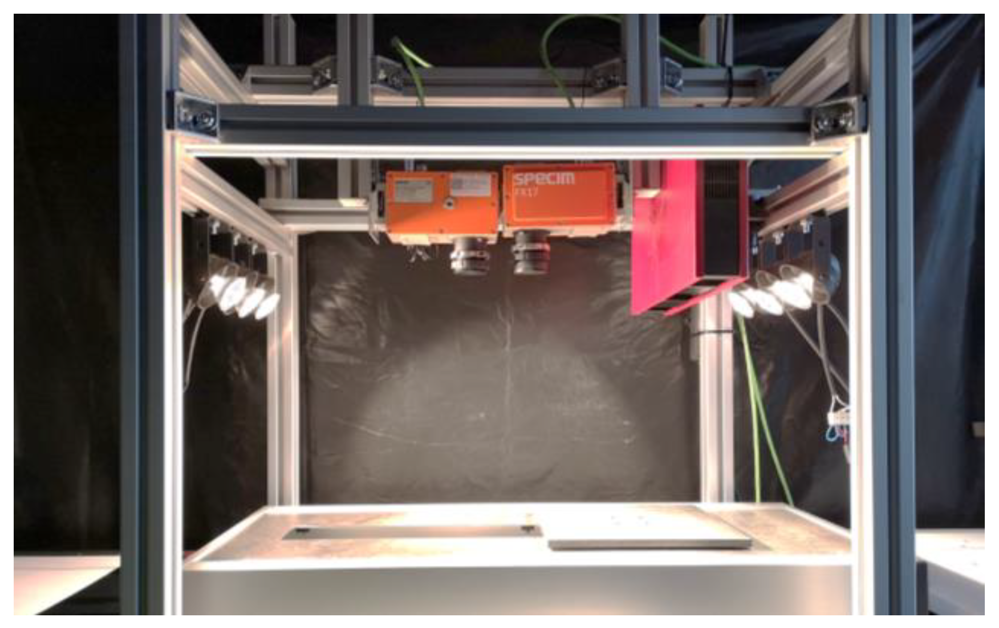
The measurement setup shown in Figure 2 consists of two Specim Ltd. (Oulu, Finland) hyperspectral pushbroom cameras (Specim FX10 and Specim FX17), a 3D scanner, a linear stage and an illumination unit. This system was chosen for the acquisition of real electronic waste samples consisting of plastics and PCBs from the landfill. Accordingly, these objects are damaged and dirty. Special attention was paid to the choice of PCBs with different mounted electronic components. The required wavelength is limited to the NIR range, therefore only the Specim FX17, working in the range from 900 nm to 1700 nm (224 bands), is used for the measurements in this work. Acquired datasets are radiometrically normalized by using dark reference image for dark-current (closed shutter) and a white reference image to reduce the influence of the intensity variability. For the white calibration a 99% reflectance tile was used.
For the acquisition of the geometry, a structured light scanner from GOM GmbH (Braunschweig, Germany) is used. The Atos Core 500 is a high-resolution optical system with a maximum resolution of 0.195 mm and a depth accuracy of 0.05 mm. This 3D scanner consists of two stereoscopic cameras with 5-megapixel resolution and a blue LED light projector which projects structured light onto the object. The projected light, which essentially encodes the surface of the object, is captured by the cameras and triangulation is used to obtain the necessary 3D information.
2.2. Combining Spectral and Spatial Data Sets
The first step of the proposed framework is the fusion of the datasets (shown in Figure 3) consisting of HSI and 3D point cloud. This is achieved by using tie points. Due to the technical setup of the sensors (fixed sensors looking vertically downwards), the objects are successively captured during one measuring process in both hyperspectral as well as three-dimensional. The transformation parameters are estimated by using tie points that are existing in both datasets and allow the fusion in x-y plane. Due to the different resolutions of the datasets, the assignment between 3D point and spectral signature is made pixel by pixel checking the neighborhood. The result is a 3D point cloud presented in Figure 4 with a spectral signature for each individual 3D point. Even though the sensor technology presented in Figure 2 would not be readily applicable in an industrial context due to the 3D sensor technology used, the potential for the overall concept of the measurement system and fusion strategy for use in industrial practice is given.
2.3. Processing of 3D Point Cloud
In these merged data sets the spatial component directly helps to simplify the problem as we can reduce the data set to regions of interest, such as the objects, and remove useless regions, such as the background. The second step of the proposed framework consists in removing the background. In our study case, the background can be easily removed using the depth information thanks to a plane estimation method. This has several advantages. Firstly, the amount of data are reduced, which has a positive effect on the further processing steps. Secondly, other disturbing effects such as dirt (e.g., on the conveyor belt) and shadow areas are removed. Areas of shadow in particular can have a negative impact on the quality of the results. An example for disturbing shadow effects and the influence on the classification result is shown in Figure 5. Shadow areas occur mainly on the border of 3D objects and also on the border of 3D components on the top of PCBs. The most disturbing shadows are on the border of the objects. Shadow areas are generally a problem when processing datasets as they reduce the reliability and success rate of algorithms for object recognition, classification and other types of processing. The removal of shadow areas is therefore an essential step towards improving image quality [27,28] and thus also improve the base for further analysis steps.
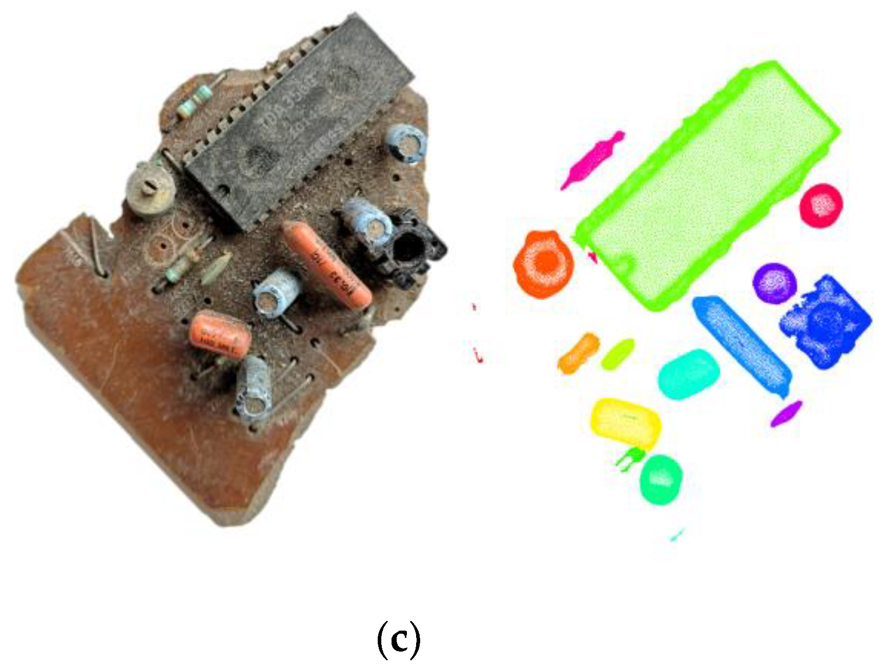
Another advantage of adding 3D data is the possibility to partition the dataset by using cluster methods, which are addressing the shape content of objects. The aim of a cluster analysis is to find structures in a set of arbitrary data with different properties and to discover relationships in order to be able to group objects. This involves forming groups in such a way that the properties of the data within the group or cluster are approximately identical. A variety of cluster algorithms exists in the state of the art for this purpose. The task of cluster algorithms is to form clusters within datasets. Clustering methods differ in their approaches and strategies. This allows the separation of the individual objects in the dataset. Due to the homogeneous data available in our dataset, a cluster approach based on Euclidean distance was chosen for the separation of the individual objects. Cluster methods can be not only used for the individual object’s separation (such as plastics and PCBs, as shown in Figure 6b), but also can be used for the separation of components on the boards (as shown in Figure 6c).
2.4. Rules-Based Classification
The third step of the proposed framework consists in defining rules to process 3D data and spectral data in order to classify individual 3D point clouds.
Based on the existing dataset, it can be stated that the hyperspectral point cloud contains valuable geometric information that is implicitly represented by the spatial arrangement of the individual 3D point clouds. In addition to the geometric information, the dataset also contains valuable spectral information to describe the physical property of the objects.
3D point clouds are a representation of spatial 3D information, which can be described by geometric characteristics. The derivation of these geometric characteristics is done by considering the local neighborhood of each 3D point. Based on this neighborhood, invariant moments can be calculated for each point, representing the geometric properties of local 3D structures [29]. A representation of some 3D features is shown in Figure 7. The 3D features tested in this article are nowadays commonly used in lidar data processing. They are based on normal vectors and eigenvalue-based 3D features like linearity, verticality, planarity, scattering, omnivariance, anisotropy, eigenentropy and change in curvature [30].
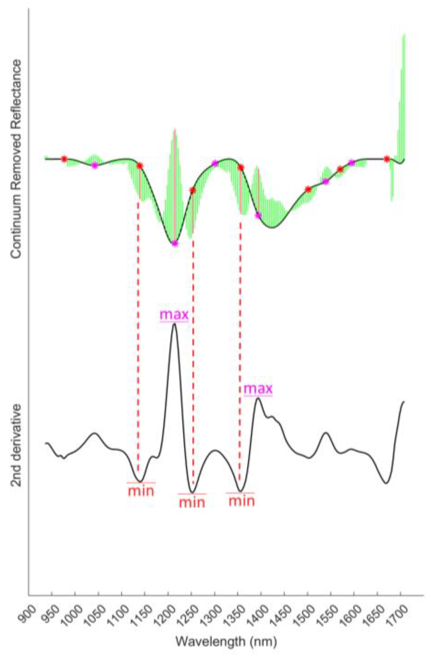
For the characterization of the spectral components, shape-describing features introduced in [31] are used. Materials can be uniquely identified by their spectral signature. Changes in material compositions lead to changes in the spectral signature and consequently to local changes in the geometric shape of these spectra. We have shown in [31] that curvature is a suitable geometric feature and allows a detailed description of spectral signatures. Mathematically, the curvature can be determined by Equation (1) using the 1st and 2nd derivative for each point where x characterizes the wavelength (in nm), y the reflectance and t the sample value, respectively.
The approach to determine the significant parameters for the description of the spectral shape is presented in Figure 8. It is based on the computation of extreme values of the 2nd derivative. For a better quantification of absorption peaks, the spectral signatures are normalized by using Continuum Removal [32,33].
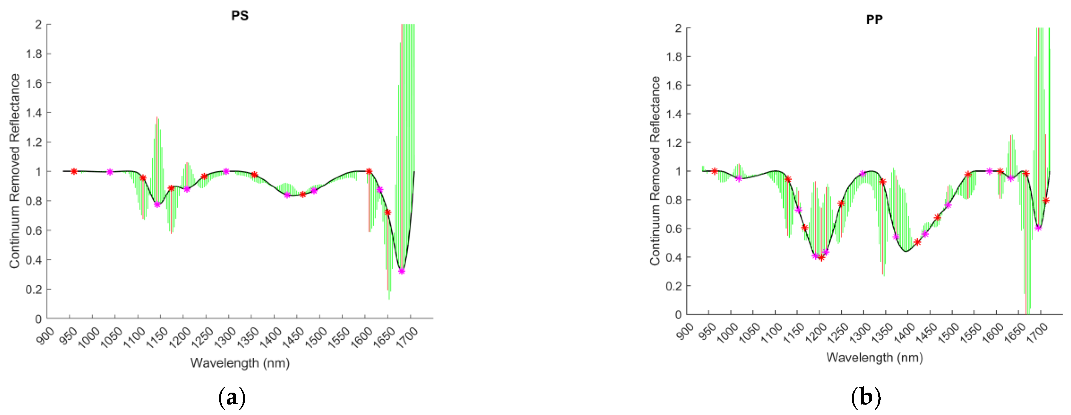
In Figure 9, the normalized spectra and the calculated curvatures for polystyrene (PS) and polypropylene (PP) are shown, which express a clear difference in the spectral footprint of both materials. The length of the green and red lines indicates the strength of the curvature. In order to take only significant curvatures into account, a threshold value must be used. The red lines represent the significant bands with a curvature value higher than the defined threshold and are derived on the basis of the curvature points presented in magenta and red colored dots. The direction of the lines (positive or negative) indicates the type of curvature behavior (concave and convex curve) and is also an important source of information to describe the shape of spectral signatures. Building on these extracted parameters regarding the spectra for each material and the 3D features describing the geometric domain, a collection of conditions can be used for classification. The combined use of both domains in particular allows to mutually support the content of each individual domain. For example, 3D features are mainly used in rule formation when the spectral information does not provide enough information (e.g., black objects on PCB). These include, for example, microchips. If the rules in the spectral domain do not produce any results, geometric rules are then checked. In the case of microchips, which are geometrically rectangular and have a planar surface, the rule is defined as follows.
A rule formation should follow a logical approach and be based on the characteristics of the objects. As example, in the case of the microchip, the feature ‘change in curvature’ is used to detect the planar surface of the object. This means that the threshold value for this characteristic must be set low, because a planar surface has no curvature. The thresholds used in our approach (threshold A = 10 and threshold B = 0.045) were empirically determined by investigations based on the underlying dataset. In the case of a different data basis due to different sensor technology, it would only be necessary to adjust the thresholds, as the features used reflect the characteristics of the objects.
To better illustrate the rule formation in the spectral domain, we refer to the example of the spectral curves of PP and PS from Figure 9 and express the resulting rule as shown in Listing 1.
Listing 1. Shape-based Rule for PS and PP.
| AND AND AND AND AND | AND AND AND AND AND |
The rule for each material includes a number of conditions. Each of these conditions is based on the Curvature Value (CV) at a specific band and the sign of the curvature value. If the sign is negative, the curvature behavior is concave and CV must be smaller than the defined threshold value. For a convex curvature behavior, the sign is positive, i.e., the curvature value must be greater than the defined threshold value.
As mentioned before, for rule formation, mainly the significant bands with high curvature value are considered (red lines). Each significant band leads to a condition. By analyzing the spectra beforehand, the number of conditions can be reduced to a minimum and not all significant curvature values (red lines) have to be taken into account. Therefore, only six conditions are defined for sample PS in Listing 1, while in Figure 9 a total of seven red lines are present. An overview of the used spectra for the rule-formation is given in Figure 10.
3. Results
This section shows the steps of the rule-based classification. For a better understanding, an overview of the process is shown in Figure 11. It can be understood as an iterative refinement starting with simple and dominant conditions and continuing in the direction of more complex and composite conditions. The first step of the classification process is based on the knowledge about the spectral behavior of plastics, which is significantly different to those of PCBs. We use this knowledge to separate these two groups and check the average spectrum for each cluster. Since plastic objects are usually made of one material and not of a combination of materials as for PCBs (board and different components), the average spectrum provides a good approach to classify the objects in question (Figure 12). This procedure not only ensures a clean classification of these objects, but also offers advantages in terms of performance, as not every single pixel has to be checked.
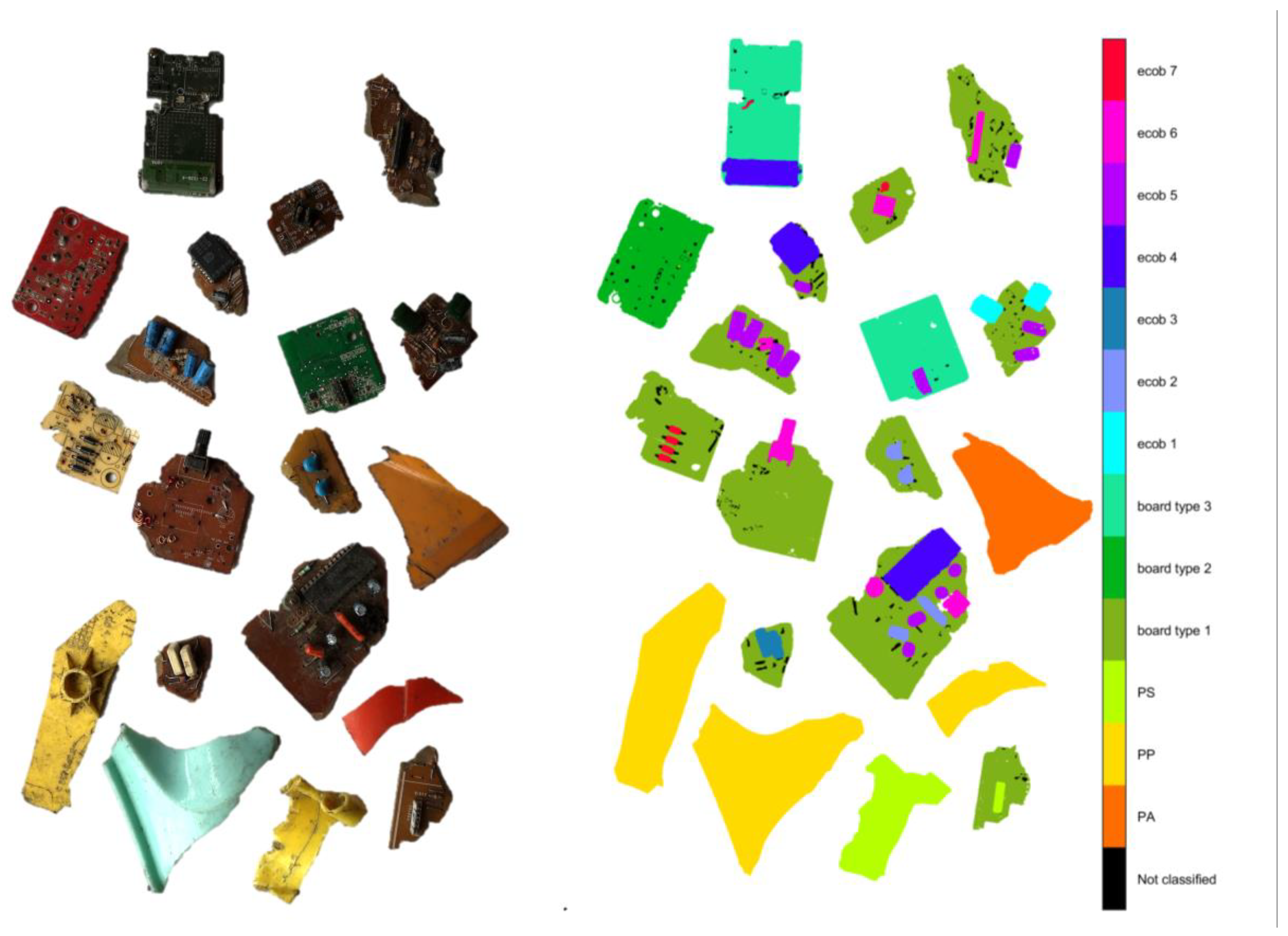
By assuming that all unclassified objects are objects consisting of composite materials, the classification of clusters can be refined in the next step. The knowledge about the objects allows us to adapt our approach to the characteristics of the objects; in this case, circuit boards. That means, the PCBs are separated into individual parts consisting of the board (a plane surface) and the individual electronic components on the board (ecob). The separation between board and components is based on plane estimation [34], while the components on the board are again processed based on Euclidean distance clustering. Next, once again, a rule check of the average spectra for each cluster (board and board components) is carried out. As a result (see example shown in Figure 13) the areas that were divided into boards and components can now be subdivided according to their material properties. In the example dataset, we thus obtain a classification of three different board types, three different types of capacitors and a connector consisting of the material polystyrene (PS).
All other existing components do not provide clean spectra that can be used for classification, either because of the black coloring (high absorption) or because of the material composition (metals). However, they are surrounded by detected and classified elements. This relation can be expressed by geometric and topological features allowing to further refine the classification. Figure 14 shows an example of results where a total of four additional groups of components were classified. The four groups include round capacitors, rectangular planar objects (such as microchips), resistors and other components (such as potentiometers and connectors). Especially in this case of classification based on geometric features, it can be seen that the classification of board components is challenging, particularly when dealing with dirty and damaged elements. Even though most of the components have been correctly classified, it can be seen, for example, that one of the connectors has been assigned to the class of radial capacitors (ecob 5). This is due to geometrical similarities shown in Figure 15.
The smaller the objects are, the more important it is to use 3D sensors that allow a high-resolution detection so that even the smallest objects can still be captured in detail. In this context, it is also important to mention that the sensors chosen for data acquisition should always be selected in accordance with the application. Capturing small objects with a low-resolution 3D scanner will not give satisfactory results. This is also reflected in the statistics computed for each class shown in Table 1. With decreasing object size, an exact classification becomes more difficult. For the calculation of the statistics, the underlying dataset was manually annotated and used for the computation of the confusion matrix. The overall statistics for the entire dataset are shown in Table 2. It can be stated that with an Overall Accuracy (OA) of 98.24%, a satisfactory result is achieved.
For comparison purposes, a SVM based classification (C-SVC, RBF-Kernel, C: 2048, gamma: 2.8284), which is one of the most widely used pixel-wise classifiers, was additionally performed. The SVM method was implemented in MATLAB using the LIBSVM library [35]. The optimization of the hyperparameters was determined by a 10-fold cross-validation. For the training data set, 10% of samples of each class were randomly selected. The main purpose of the comparison is to show, that an approach, combining 3D and HSI, has advantages in terms of classification. The results of the SVM classification are also shown in Table 2. Considering the statistics, it is clearly evident that a classification processing 3D and HSI data outperforms a SVM classification based only on HSI.
4. Discussion
The results presented in Section 3 show significant added value of a combined use of 3D and HSI for classification of waste PCBs. In order to get the maximum benefit from such a combination, it is important for the strategic approach to analyze the underlying data sufficiently. A well-developed knowledge base with regard to the characteristics of objects helps to improve the results. Especially the addition of the 3D information is helpful in structuring and simplifying the datasets (background removal, removal of shadows, separation between objects). Hyperspectral data, on the other hand, help to determine the type of material and thus refines the classification. Even more important, each of the very different datasets supports the other and compensates the weaknesses of the other. Many of the components that are mounted on circuit boards have a black material color. The use of purely spectral information is not appropriate in these cases due to the high absorption of light. This is also confirmed by the SVM comparison (Table 2), where only HSI data were used for classification. A purely 3D-based classification can be successful in separating objects (e.g., board and components on board), but it would fail, for example, in differentiating between different board materials or compositions.
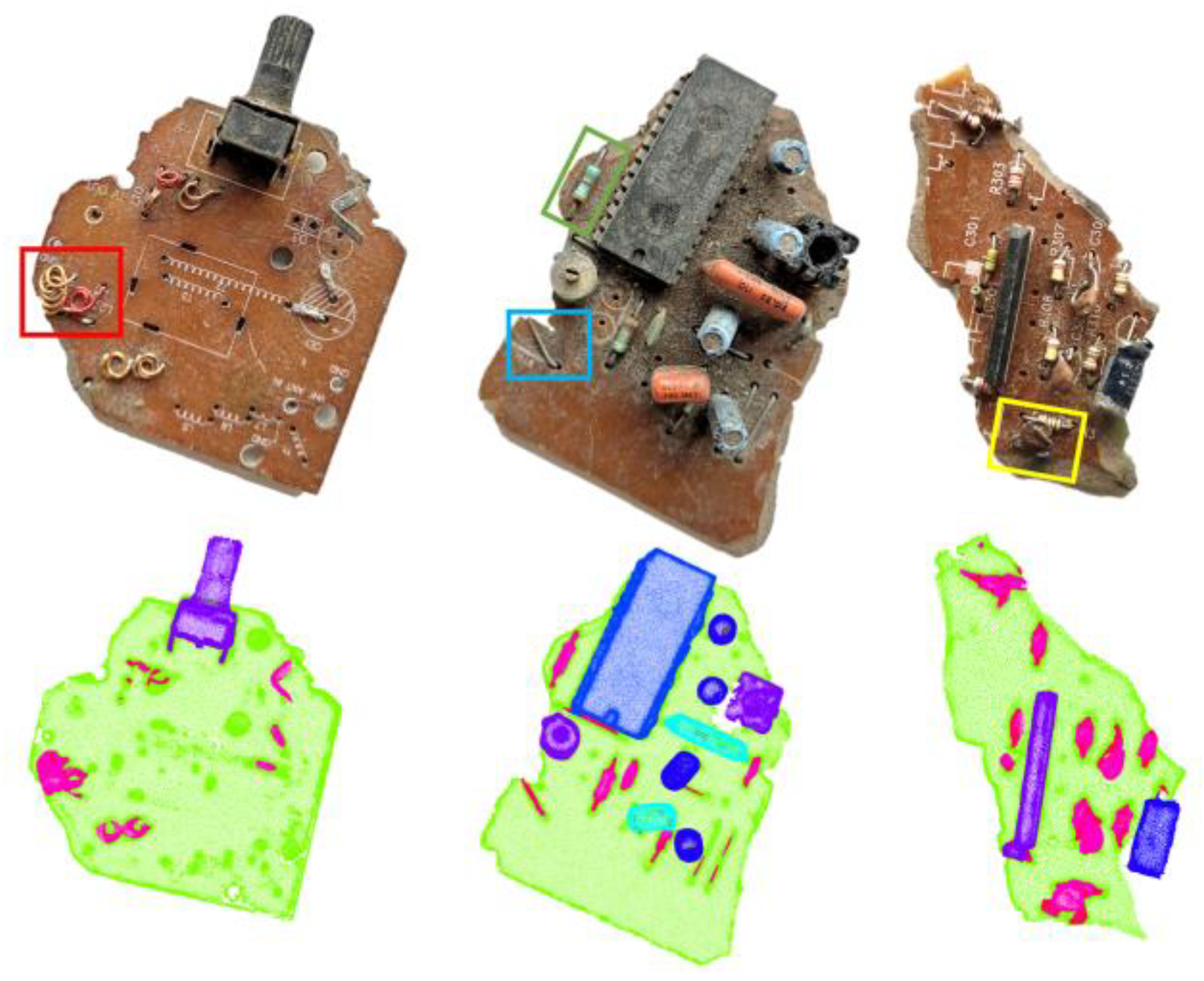
Especially with 3D data, the resolution and accuracy of the dataset used plays a major role. The higher the resolution, the more accurate the description of very fine, small objects on the board. We see in our experiments that we reach our limits with objects shown in Figure 16 and that a clean separation of small elements such as metals (red and blue box), resistors (green box) and capacitors (yellow box) is not successful. Nevertheless, even if a distinction between these elements does not seem possible in detail, these elements can be identified as components of PCBs through the given topological relationships, which could provide an advantage for further analyses (e.g., determination of different metals).
The classification map shown in Figure 14 is the result of a total of 13 defined rules and works well for the materials and components in the used dataset. An extension to further objects and materials needs the exploitation of their characteristics and the definition of additional rules. This has to be completed carefully in order to avoid conflicting definitions and needs the existence of spatial and spectral characteristics allowing to differentiate further object types. However, the iterative strategy going from more dominant to fewer dominant rules has shown, that even smallest elements can be separated with acceptable accuracy. This is already a reliable base for further extensions. Nevertheless, it is necessary to pay attention to correct modelling, and thus it is important to study the spatial and spectral properties of the objects beforehand and to investigate to what extent the acquired data can make these properties visible. Generally, when setting up rules, it is important to avoid overfitting. Thresholds that are overly sensitive can result in incorrect classifications when applied to new datasets and should therefore be chosen carefully. In addition, the underlying 3D data quality must be considered when forming rules based on 3D geometry. As example, in this article the parameters and thresholds for rule formation were chosen with regard to the used sensor system and the resulting point cloud. In the case of a different 3D sensor with another resolution, accuracy and noise behavior, it would be necessary to adjust the parameters.
Another aspect to consider is the performance of the system and the assessment of use in industrial practice. We are aware that the use in industrial practice poses certain challenges such as high-speed processing, an appropriate integration of the sensor technology into the sorting process and also the handling of dust and dirt in an industrial context is a factor that should not be underestimated. This means that the sensor technology used and the acquisition and processing strategy must meet these requirements. The approach proposed in this article has the potential to fulfil these demands, but certain modifications with regard to the 3D sensor technology are necessary. The strategy of the approach (sensors for acquisition, registration approach and data processing) is general and is mainly affected by the specifications and the capacity of the senor technology used. The structured light scanner used in this article is not advisable in the context of a sorting process due to the needed fast processing speed. However, it has the benefit to produce high quality 3D data, which in turn is advantageous in the context of small objects. The use of such a sensor system would therefore be recommended in the context of randomized quality checks where speed is not important.
However, there are alternatives that are suitable for use in production lines [36,37]. The study of [38] investigates the applicability of 3D sensor technologies in the context of production lines. As a result, four techniques for capturing 3D data in the context of industrial applications were identified, namely laser triangulation, time-of-flight (ToF), shape-from-focus (SFF) and stereovision [38]. Mainly laser scanners based on triangulation are widely used in production lines. Such systems are able to achieve depth resolutions down to the range of a few micrometers and are a robust and standardized technology that could also be used in the context of the proposed approach.
The use of hyperspectral sensors in industrial applications is also conceivable and is particularly widespread in the food industry [39,40,41]. The Specim FX17 sensor used was able to detect 670 FPS at full resolution. It is not always necessary to use the full resolution. By analyzing the data beforehand, spectral ranges or even only a small number of bands can be used, which ultimately leads to a further increase in the detection rate. Important in the context of hyperspectral sensor technology is the illumination unit. This must be installed in the measurement setup in such a way that the 3D technology used is not influenced.
At this point we would also like to briefly discuss the influence of object soiling on the measurements of the hyperspectral sensors, since in practice it is precisely such objects that are involved. Dirt on objects influences the reflectance on the surface of the objects. This inevitably leads to changes and shifts in the spectral signatures as can be seen in Figure 17 for one of the samples in the used dataset. That our proposed approach is robust to such influences can be seen from the achieved results. This is due to two main facts: First, we use spectral features that describe the shape of spectral signatures, even if the expression of absorption or reflectance peaks is low due to the weak reflectance, the shape of the spectral signature remains the same. Thus, the defined rules based on the shape apply in both cases. The second point is due to the 3D component. Through the 3D information we can group components in clusters and for the rule check we refer to the average spectral signature of this cluster. Thus, the influence of dirty areas is only significant if the object is completely soiled.
The processing time of the data is also a factor that needs to be taken into account. The 3D processing and point-by-point checking for conditions using MATLAB on a machine with an Intel(R) Core(TM) i7-10700 CPU @ 2.90GHz and 16 GB RAM was 110.29 s for the background removed dataset (752.253 3D points and 224 bands) shown in Figure 4. For comparison, processing the same dataset (only HSI) on the same machine using SVM (LIBSVM for MATLAB) requires 2025.07 s.
For a practical application, 110.29 s is considered high. However, in this context it must also be considered that a full spectral and high-resolution 3D point cloud serves as the data basis. Optimizations in terms of processing time is conceivable and could be achieved by reducing the data basis (e.g., reduction of spectral resolution), by using more powerful hardware and by more efficient programming (e.g., parallel computing).
5. Conclusions
In this paper, a combined dataset consisting of a 3D point cloud and an HSI was used to classify different types of materials and objects of electronic waste. In addition to the classification of different plastic materials, it has been shown that a combination of geometric and physical information can also help to distinguish components on circuit boards, such as capacitors, transistors and other small parts on board. Using a rule-based classification approach leads to satisfying results with an OA of 98.24%. The comparison with an SVM approach based only on spectral information results in an OA of 88.65% and confirms that a combined dataset helps to improve the quality of classification.
Author Contributions
Conceptualization, S.P., A.T. and F.B.; Investigation, S.P.; Methodology, S.P., A.T. and F.B.; Supervision, A.T. and F.B.; Writing—original draft, S.P.; Writing—review and editing, A.T. and F.B.; All authors have read and agreed to the published version of the manuscript.
Funding
This research was funded by the European Union from the European Regional Development Fund and the state of Rhineland-Palatinate.
Institutional Review Board Statement
Not applicable.
Informed Consent Statement
Not applicable.
Acknowledgments
We thank Pellenc ST for supplying the real waste materials.
Conflicts of Interest
The authors declare no conflict of interest. The funders had no role in the design of the study; in the collection, analyses, or interpretation of data; in the writing of the manuscript, or in the decision to publish the results.
References
- Forti, V.; Baldé, C.; Kuehr, R.; Bel, G. The Global E-Waste Monitor 2020: Quantities, Flows, and the Circular Economy Potential; United Nations University (UNU); United Nations Institute for Training and Research (UNITAR)–co-hosted SCYCLE Programme; International Telecommunication Union (ITU); International Solid Waste Association (ISWA): Bonn, Germany; Geneva, Switzerland; Rotterdam, The Netherlands, 2020; ISBN 978-92-808-9114-0. [Google Scholar]
- Calvini, R.; Ulrici, A.; Amigo, J.M. Growing applications of hyperspectral and multispectral imaging. Des. Optim. Org. Synth. 2020, 32, 605–629. [Google Scholar] [CrossRef]
- Li, W.; Esders, B.; Breier, M. SMD segmentation for automated PCB recycling. In Proceedings of the 2013 11th IEEE International Conference on Industrial Informatics (INDIN), Bochum, Germany, 29–31 July 2013; pp. 65–70. [Google Scholar]
- Jessurun, N.T.; Paradis, O.P.; Tehranipoor, M.; Asadizanjani, N. SHADE: Automated Refinement of PCB Component Estimates Using Detected Shadows. In Proceedings of the 2020 IEEE Physical Assurance and Inspection of Electronics (PAINE), Washington, DC, USA, 28–29 July 2020; Institute of Electrical and Electronics Engineers (IEEE): Piscataway, NJ, USA, 2020; pp. 1–6. [Google Scholar]
- Herchenbach, D.; Li, W.; Breier, M. Segmentation and classification of THCs on PCBAs. In Proceedings of the 2013 11th IEEE International Conference on Industrial Informatics (INDIN), Bochum, Germany, 29–31 July 2013; Institute of Electrical and Electronics Engineers (IEEE): Piscataway, NJ, USA, 2013; pp. 59–64. [Google Scholar]
- Li, D.; Li, C.; Chen, C.; Zhao, Z. Semantic Segmentation of a Printed Circuit Board for Component Recognition Based on Depth Images. Sensors 2020, 20, 5318. [Google Scholar] [CrossRef]
- Khan, M.J.; Khan, H.S.; Yousaf, A.; Khurshid, K.; Abbas, A. Modern Trends in Hyperspectral Image Analysis: A Review. IEEE Access 2018, 6, 14118–14129. [Google Scholar] [CrossRef]
- Ibrahim, A.; Tominaga, S.; Horiuchi, T. Spectral imaging method for material classification and inspection of printed circuit boards. Opt. Eng. 2010, 49, 057201. [Google Scholar] [CrossRef]
- Palmieri, R.; Bonifazi, G.; Serranti, S. Recycling-oriented characterization of plastic frames and printed circuit boards from mobile phones by electronic and chemical imaging. Waste Manag. 2014, 34, 2120–2130. [Google Scholar] [CrossRef]
- Sudharshan, V.; Seidel, P.; Ghamisi, P.; Lorenz, S.; Fuchs, M.; Fareedh, J.S.; Neubert, P.; Schubert, S.; Gloaguen, R. Object Detection Routine for Material Streams Combining RGB and Hyperspectral Reflectance Data Based on Guided Object Localization. IEEE Sens. J. 2020, 20, 11490–11498. [Google Scholar] [CrossRef]
- Ghamisi, P.; Plaza, J.; Chen, Y.; Li, J.; Plaza, A.J. Advanced Spectral Classifiers for Hyperspectral Images: A review. IEEE Geosci. Remote Sens. Mag. 2017, 5, 8–32. [Google Scholar] [CrossRef] [Green Version]
- Andrés, S.; Arvor, D.; Mougenot, I.; Libourel, T.; Durieux, L. Ontology-based classification of remote sensing images using spectral rules. Comput. Geosci. 2017, 102, 158–166. [Google Scholar] [CrossRef]
- Berhane, T.M.; Lane, C.R.; Wu, Q.; Autrey, B.C.; Anenkhonov, O.A.; Chepinoga, V.V.; Liu, H. Decision-Tree, Rule-Based, and Random Forest Classification of High-Resolution Multispectral Imagery for Wetland Mapping and Inventory. Remote Sens. 2018, 10, 580. [Google Scholar] [CrossRef] [Green Version]
- Cui, W.; Yao, M.; Hao, Y.; Wang, Z.; He, X.; Wu, W.; Li, J.; Zhao, H.; Xia, C.; Wang, J. Knowledge and Geo-Object Based Graph Convolutional Network for Remote Sensing Semantic Segmentation. Sensors 2021, 21, 3848. [Google Scholar] [CrossRef]
- Ghazaryan, G.; Dubovyk, O.; Löw, F.; Lavreniuk, M.; Kolotii, A.; Schellberg, J.; Kussul, N. A rule-based approach for crop identification using multi-temporal and multi-sensor phenological metrics. Eur. J. Remote Sens. 2018, 51, 511–524. [Google Scholar] [CrossRef]
- Houhoulis, P.F.; Michener, W. Detecting wetland change: A rule-based approach using NWI and SPOT-XS data. Photogramm. Eng. Remote Sens. 2000, 66, 205–211. [Google Scholar]
- Liu, S.; Shi, Q. Multitask Deep Learning with Spectral Knowledge for Hyperspectral Image Classification. IEEE Geosci. Remote Sens. Lett. 2020, 17, 2110–2114. [Google Scholar] [CrossRef] [Green Version]
- Ponciano, J.-J.; Roetner, M.; Reiterer, A.; Boochs, F. Object Semantic Segmentation in Point Clouds—Comparison of a Deep Learning and a Knowledge-Based Method. ISPRS Int. J. Geo. Inf. 2021, 10, 256. [Google Scholar] [CrossRef]
- Dvorak, R.; Kosior, E.; Moody, L. Development of NIR Detectable Black Plastic Packaging. Available online: http://www.wrap.org.uk/sites/files/wrap/Recyclability_of_Black_Plastic_Summary.pdf (accessed on 11 January 2021).
- Rozenstein, O.; Puckrin, E.; Adamowski, J. Development of a new approach based on midwave infrared spectroscopy for post-consumer black plastic waste sorting in the recycling industry. Waste Manag. 2017, 68, 38–44. [Google Scholar] [CrossRef]
- Roscher, R.; Behmann, J.; Mahlein, A.-K.; Dupuis, J.; Kuhlmann, H.; Plümer, L. Detection of disease symptoms on hyperspectral 3D plant models. ISPRS Ann. Photogramm. Remote Sens. Spat. Inf. Sci. 2016, III-7, 89–96. [Google Scholar] [CrossRef] [Green Version]
- Morsy, S.; Shaker, A.; El-Rabbany, A. Multispectral LiDAR Data for Land Cover Classification of Urban Areas. Sensors 2017, 17, 958. [Google Scholar] [CrossRef] [Green Version]
- Igelbrink, F.; Wiemann, T.; Pütz, S.; Hertzberg, J. Markerless Ad-Hoc Calibration of a Hyperspectral Camera and a 3D Laser Scanner. In Advances in Intelligent Systems and Computing; Springer Science and Business Media LLC: Berlin, Germany, 2018; pp. 748–759. [Google Scholar]
- Nieto, J.I.; Monteiro, S.T.; Viejo, D. 3D geological modelling using laser and hyperspectral data. IEEE Int. Geosci. Remote Sens. Symp. 2010, 4568–4571. [Google Scholar] [CrossRef]
- Wendel, A.; Underwood, J. Extrinsic Parameter Calibration for Line Scanning Cameras on Ground Vehicles with Navigation Systems Using a Calibration Pattern. Sensors 2017, 17, 2491. [Google Scholar] [CrossRef] [Green Version]
- Tan, P.-N.; Steinbach, M.; Karpatne, A.; Kumar, V. Introduction to Data Mining, 2nd ed.; Pearson: New York, NY, USA, 2019; ISBN 9780133128901. [Google Scholar]
- Shahtahmassebi, A.; Yang, N.; Wang, K.; Moore, N.; Shen, Z. Review of shadow detection and de-shadowing methods in remote sensing. Chin. Geogr. Sci. 2013, 23, 403–420. [Google Scholar] [CrossRef] [Green Version]
- Mostafa, Y. A Review on Various Shadow Detection and Compensation Techniques in Remote Sensing Images. Can. J. Remote Sens. 2017, 43, 545–562. [Google Scholar] [CrossRef]
- Weinmann, M.; Jutzi, B.; Mallet, C. Feature relevance assessment for the semantic interpretation of 3D point cloud data. ISPRS Ann. Photogramm. Remote Sens. Spat. Inf. Sci. 2013, II-5/W2, 313–318. [Google Scholar] [CrossRef] [Green Version]
- Weinmann, M.; Jutzi, B.; Hinz, S.; Mallet, C. Semantic point cloud interpretation based on optimal neighborhoods, relevant features and efficient classifiers. ISPRS J. Photogramm. Remote Sens. 2015, 105, 286–304. [Google Scholar] [CrossRef]
- Polat, S.; Tremeau, A.; Boochs, F. Rule-Based Classification of Hyperspectral Imaging Data. 2021. Available online: http://arxiv.org/pdf/2107.10638v1 (accessed on 9 August 2021).
- Clark, R.N.; Swayze, G.A.; Livo, K.E.; Kokaly, R.; Sutley, S.J.; Dalton, J.B.; McDougal, R.R.; Gent, C.A. Imaging spectroscopy: Earth and planetary remote sensing with the USGS Tetracorder and expert systems. J. Geophys. Res. Space Phys. 2003, 108. [Google Scholar] [CrossRef]
- Clark, R.N.; Roush, T.L. Reflectance spectroscopy: Quantitative analysis techniques for remote sensing applications. J. Geophys. Res. Space Phys. 1984, 89, 6329–6340. [Google Scholar] [CrossRef]
- Torr, P.; Zisserman, A. MLESAC: A New Robust Estimator with Application to Estimating Image Geometry. Comput. Vis. Image Underst. 2000, 78, 138–156. [Google Scholar] [CrossRef] [Green Version]
- Chang, C.-C.; Lin, C.-J. LIBSVM: A library for support vector machines. ACM Trans. Intell. Syst. Technol. 2011, 2, 1–27. [Google Scholar] [CrossRef]
- Bian, S.; Zhou, P.; Xu, J.; Zhang, J.; Shan, D. On-line detection device for high temperature forgings based on laser triangulation. J. Phys. 2021, 1885, 052035. [Google Scholar] [CrossRef]
- Sioma, A. Automated Control of Surface Defects on Ceramic Tiles Using 3D Image Analysis. Materials 2020, 13, 1250. [Google Scholar] [CrossRef] [Green Version]
- Sioma, A. 3D imaging methods in quality inspection systems. In Photonics Applications in Astronomy, Communications, Industry, and High-Energy Physics Experiments 2019; Romaniuk, R.S., Linczuk, M., Eds.; SPIE: Wilga, Poland, 2019; p. 91. ISBN 9781510630659. [Google Scholar]
- Al-Sarayreh, M.; Reis, M.M.; Yan, W.Q.; Klette, R. Detection of Red-Meat Adulteration by Deep Spectral–Spatial Features in Hyperspectral Images. J. Imaging 2018, 4, 63. [Google Scholar] [CrossRef] [Green Version]
- Boldrini, B.; Kessler, W.; Rebner, K.; Kessler, R.W. Hyperspectral Imaging: A Review of Best Practice, Performance and Pitfalls for in-line and on-line Applications. J. Near Infrared Spectrosc. 2012, 20, 483–508. [Google Scholar] [CrossRef]
- Ma, J.; Sun, D.-W.; Pu, H.; Cheng, J.-H.; Wei, Q. Advanced Techniques for Hyperspectral Imaging in the Food Industry: Principles and Recent Applications. Annu. Rev. Food Sci. Technol. 2019, 10, 197–220. [Google Scholar] [CrossRef] [PubMed]
Figure 1.
Workflow consisting of fusion, simplifying and classification steps.

Figure 2.
Measuring setup consisting of hyperspectral cameras, linear stage, illumination unit and 3D structured light scanner.
Figure 2.
Measuring setup consisting of hyperspectral cameras, linear stage, illumination unit and 3D structured light scanner.

Figure 3.
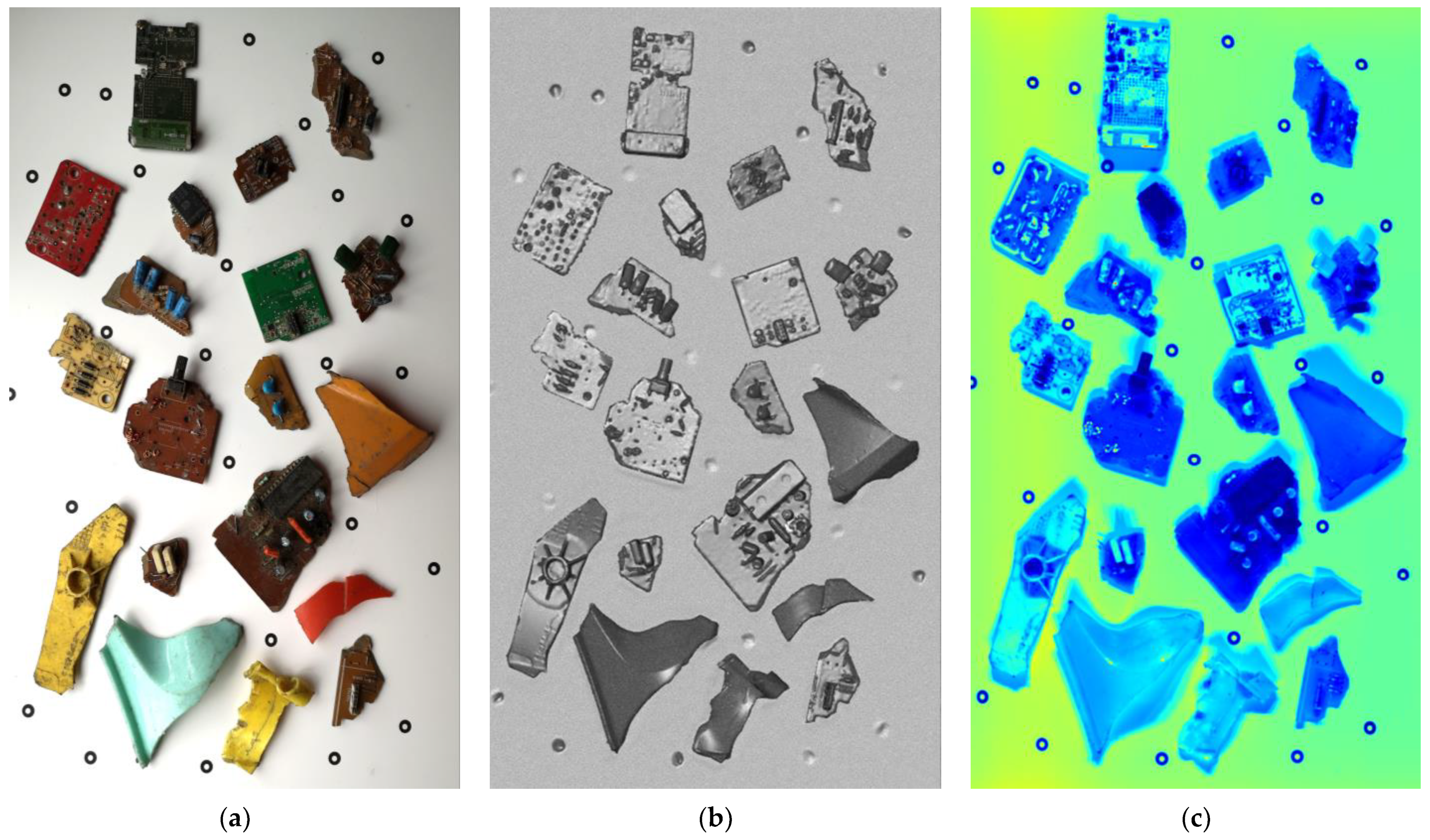
Acquired datasets of electronic waste consisting of waste plastics and PCBs: (a) RGB; (b) 3D point cloud with a resolution of 0.5 mm and a depth accuracy of 0.05 mm; (c) HSI with a resolution of 636 × 1118 pixels and 224 bands in the wavelength range from 900 nm to 1700 nm.
Figure 3.
Acquired datasets of electronic waste consisting of waste plastics and PCBs: (a) RGB; (b) 3D point cloud with a resolution of 0.5 mm and a depth accuracy of 0.05 mm; (c) HSI with a resolution of 636 × 1118 pixels and 224 bands in the wavelength range from 900 nm to 1700 nm.

Figure 4.
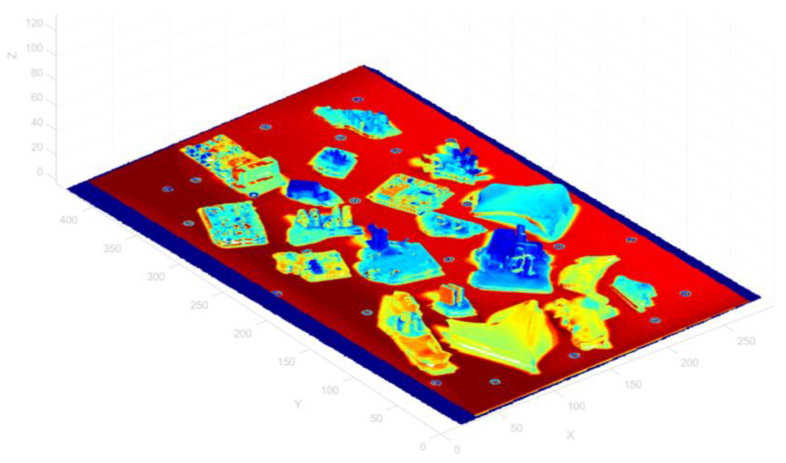
Combined 3D point cloud and HSI. Each 3D point is assigned by a spectrum. In this figure, the average value over the entire spectrum is shown per pixel.
Figure 4.
Combined 3D point cloud and HSI. Each 3D point is assigned by a spectrum. In this figure, the average value over the entire spectrum is shown per pixel.

Figure 5.
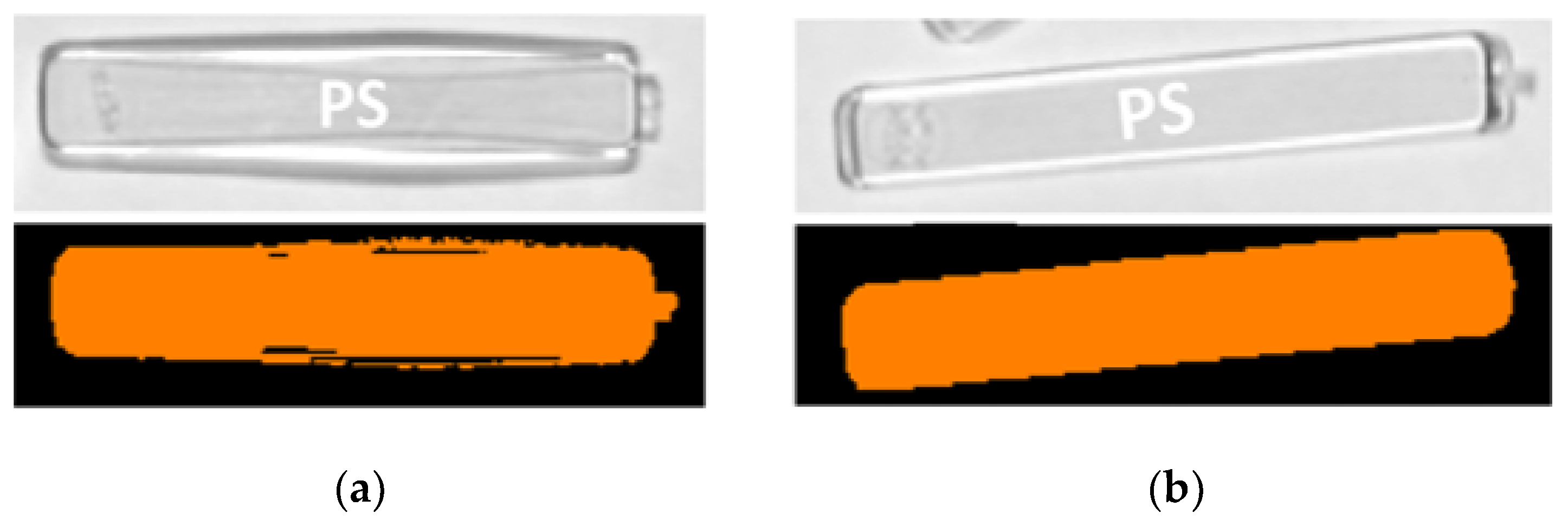
Influence of shadow on the classification process. Here shadow occurs only on the neighboring area surrounding the object. (a) Classification of pixels values belonging to the class PS using spectral data. (b) Classification of pixels values belonging to the class PS after removal of the background.
Figure 5.
Influence of shadow on the classification process. Here shadow occurs only on the neighboring area surrounding the object. (a) Classification of pixels values belonging to the class PS using spectral data. (b) Classification of pixels values belonging to the class PS after removal of the background.

Figure 6.
Examples of results of 3D point cloud clustering: (a) Background removed dataset; (b) Clustered objects; (c) PCB with electronic components and clustering result. The clustering is completed after removing the board points using a plane estimation method.
Figure 6.
Examples of results of 3D point cloud clustering: (a) Background removed dataset; (b) Clustered objects; (c) PCB with electronic components and clustering result. The clustering is completed after removing the board points using a plane estimation method.


Figure 7.
Visualization of 3D features. Omnivariance (left), Verticality (middle) and Normal Change Rate (right).
Figure 7.
Visualization of 3D features. Omnivariance (left), Verticality (middle) and Normal Change Rate (right).

Figure 8.
Use of minimum and maximum positions of 2nd derivative to select significant parameters for shape description. Parameters are the location (min/max), the curvature values at these locations (red lines) and the direction of curvature value (up for convex and down for concave behavior) [31].

Figure 9.
Continuum Removed Reflectance spectra (black line), calculated curvature values (green lines), maximum points with concave behavior (red dots) and minimum points with convex behavior (magenta dots) for (a) Polystyrene (PS); (b) Polypropylene (PP) [31].
Figure 9.
Continuum Removed Reflectance spectra (black line), calculated curvature values (green lines), maximum points with concave behavior (red dots) and minimum points with convex behavior (magenta dots) for (a) Polystyrene (PS); (b) Polypropylene (PP) [31].

Figure 10.
Spectral signatures used for the classification. As a result, the rule defined for a category is specific to that category and there is no possibility of confusion because the shapes are distinct enough. Such rules can therefore only be used if the shapes of the spectral curves are all sufficiently different.

Figure 11.
Steps of the rule-based classification process using spectral and spatial features for the rule formation. The geometrical information is not only used for structuring but also supports the classification of components that cannot be classified from their spectral signature only.
Figure 11.
Steps of the rule-based classification process using spectral and spatial features for the rule formation. The geometrical information is not only used for structuring but also supports the classification of components that cannot be classified from their spectral signature only.

Figure 12.
Example of result of classification (after step 1) of plastic objects by checking average spectra for each cluster.
Figure 12.
Example of result of classification (after step 1) of plastic objects by checking average spectra for each cluster.

Figure 13.
Result of classification for PCBs using spectral features (after step 2). Classification of three board types and four different types of components on board (PS, ecob 1, ecob 2 and ecob 3).
Figure 13.
Result of classification for PCBs using spectral features (after step 2). Classification of three board types and four different types of components on board (PS, ecob 1, ecob 2 and ecob 3).

Figure 14.
Result of classification for PCBs using 3D features (after step 3). Classification of four different types of components on board (ecob 4, ecob 5, ecob 6 and ecob 7).
Figure 14.
Result of classification for PCBs using 3D features (after step 3). Classification of four different types of components on board (ecob 4, ecob 5, ecob 6 and ecob 7).

Figure 15.
Misclassification due to geometric similarities in the point cloud.

Figure 16.
Small components such as metals (red and blue box), resistors (green box) and capacitors (yellow box) are difficult to distinguish because of limits in resolution. Nevertheless, they can be classified as components of a PCB due to the topological relationships provided by the 3D data.
Figure 16.
Small components such as metals (red and blue box), resistors (green box) and capacitors (yellow box) are difficult to distinguish because of limits in resolution. Nevertheless, they can be classified as components of a PCB due to the topological relationships provided by the 3D data.

Figure 17.
Influence of dirt on the reflectance of spectral signatures. (a) Spectra of a heavily polluted area (red box). (b) Spectra of areas without dirt (green box).
Figure 17.
Influence of dirt on the reflectance of spectral signatures. (a) Spectra of a heavily polluted area (red box). (b) Spectra of areas without dirt (green box).


Table 1.
Classification accuracies for each class based on 3D and HSI data.
| Class | OA of Single | Error of Single | F1-Score | Kappa |
|---|---|---|---|---|
| PA | 0.9969 | 0.0030 | 0.9975 | 0.9584 |
| PP | 0.9961 | 0.0380 | 0.9966 | 0.8781 |
| PS | 0.9861 | 0.0138 | 0.9794 | 0.9723 |
| Board type 1 | 0.9075 | 0.0924 | 0.9327 | 0.7950 |
| Board type 2 | 0.9560 | 0.0439 | 0.9755 | 0.9628 |
| Board type 3 | 0.9689 | 0.0311 | 0.9789 | 0.9325 |
| ecob 1 | 0.8936 | 0.1063 | 0.9240 | 0.9947 |
| ecob 2 | 0.7206 | 0.2793 | 0.7594 | 0.9947 |
| ecob 3 | 0.7764 | 0.2235 | 0.7948 | 0.9970 |
| ecob 4 | 0.9849 | 0.0150 | 0.9094 | 0.9745 |
| ecob 5 | 0.8100 | 0.1899 | 0.7931 | 0.9848 |
| ecob 6 | 0.7114 | 0.2885 | 0.7127 | 0.9890 |
| ecob 7 | 0.6595 | 0.3404 | 0.5831 | 0.9981 |
Table 2.
Classification accuracies for real electronic wastes using (a) Rule-based approach with combined 3D and HSI dataset; (b) SVM classification (C-SVC, RBF-Kernel, C: 2048, gamma: 2.8284) with HSI dataset.
Table 2.
Classification accuracies for real electronic wastes using (a) Rule-based approach with combined 3D and HSI dataset; (b) SVM classification (C-SVC, RBF-Kernel, C: 2048, gamma: 2.8284) with HSI dataset.
| Metrics | (a) Rule-Based (3D + HSI) | (b) SVM (HSI) |
|---|---|---|
| Overall Accuracy | 0.9824 | 0.8865 |
| Precision | 0.8812 | 0.7812 |
| Sensitivity | 0.8834 | 0.6576 |
| False Positive Rate | 0.0023 | 0.0124 |
| F1-Score | 0.8810 | 0.6956 |
| Kappa | 0.8672 | 0.2011 |
Publisher’s Note: MDPI stays neutral with regard to jurisdictional claims in published maps and institutional affiliations. |
© 2021 by the authors. Licensee MDPI, Basel, Switzerland. This article is an open access article distributed under the terms and conditions of the Creative Commons Attribution (CC BY) license (https://creativecommons.org/licenses/by/4.0/).
Share and Cite
MDPI and ACS Style
Polat, S.; Tremeau, A.; Boochs, F. Combined Use of 3D and HSI for the Classification of Printed Circuit Board Components. Appl. Sci. 2021, 11, 8424. https://0-doi-org.brum.beds.ac.uk/10.3390/app11188424
AMA Style
Polat S, Tremeau A, Boochs F. Combined Use of 3D and HSI for the Classification of Printed Circuit Board Components. Applied Sciences. 2021; 11(18):8424. https://0-doi-org.brum.beds.ac.uk/10.3390/app11188424
Chicago/Turabian StylePolat, Songuel, Alain Tremeau, and Frank Boochs. 2021. "Combined Use of 3D and HSI for the Classification of Printed Circuit Board Components" Applied Sciences 11, no. 18: 8424. https://0-doi-org.brum.beds.ac.uk/10.3390/app11188424
Note that from the first issue of 2016, this journal uses article numbers instead of page numbers. See further details here.