
Coincidence Detection of EELS and EDX Spectral Events in the Electron Microscope


1
EMAT, University of Antwerp, Groenenborgerlaan 171, 2020 Antwerp, Belgium
2
NANOlab Center of Excellence, University of Antwerp, Groenenborgerlaan 171, 2020 Antwerp, Belgium
3
Ernst Ruska-Centre, Forschungszentrum Jülich, 52425 Jülich, Germany
4
Department of Chemistry, Ludwig-Maximilians-Universität München, Butenandtstrasse 5-13, 81377 Munich, Germany
*
Author to whom correspondence should be addressed.
Appl. Sci. 2021, 11(19), 9058; https://0-doi-org.brum.beds.ac.uk/10.3390/app11199058
Submission received: 25 August 2021
/
Revised: 20 September 2021
/
Accepted: 22 September 2021
/
Published: 28 September 2021
(This article belongs to the Special Issue Coherent Interactions between Electrons and Light)
Abstract
:Recent advances in the development of electron and X-ray detectors have opened up the possibility to detect single events from which its time of arrival can be determined with nanosecond resolution. This allows observing time correlations between electrons and X-rays in the transmission electron microscope. In this work, a novel setup is described which measures individual events using a silicon drift detector and digital pulse processor for the X-rays and a Timepix3 detector for the electrons. This setup enables recording time correlation between both event streams while at the same time preserving the complete conventional electron energy loss (EELS) and energy dispersive X-ray (EDX) signal. We show that the added coincidence information improves the sensitivity for detecting trace elements in a matrix as compared to conventional EELS and EDX. Furthermore, the method allows the determination of the collection efficiencies without the use of a reference sample and can subtract the background signal for EELS and EDX without any prior knowledge of the background shape and without pre-edge fitting region. We discuss limitations in time resolution arising due to specificities of the silicon drift detector and discuss ways to further improve this aspect.
1. Introduction
Transmission electron microscopy (TEM) is a well-known microscopy technique which enables resolving materials down to their atomic scale. On top of the imaging capabilities, powerful spectroscopic techniques such as electron energy-loss spectroscopy (EELS) and energy dispersive X-ray spectroscopy (EDX) are commonly used. EELS measures the energy loss of the incoming electron when it interacts with matter via the use of a magnetic prism which provides information e.g., on the elements present in the sample and their electronic structure. EDX uses the fluorescence X-rays emitted from atoms excited by the primary electron beam. These X-rays are collected, and their energy analyzed from which the energy spectrum of the emitted X-rays is obtained, holding information on the chemical content of the sample. Both techniques are often performed with a condensed electron probe that is scanned over the sample and at each position the signal is recorded. In conventional analytical TEM, the electron and X-ray signals are gathered using an integrated method where the entire signal landing on the detector is integrated for a certain exposure time which typically varies from s to seconds or even minutes. For EELS, the integration time is typically of the order of ms where the lower end is determined by the finite read out speed of the pixelated detector. In EDX, the integration time can be chosen more freely and typically ranges from s up to minutes. Modern digital pulse processors (DPP) allow analysis of not only the energy of the X-ray events, but also their time-of-arrival (TOA) [1,2,3]. For electron detection, the advent of so-called Timepix detectors [4,5] enables the detection of individual electrons on a pixelated detector with nanosecond precision. Hence compared to recording frames, the individual events are now detected from which the TOA is recorded. Placing such a detector in the detection plane of an EELS spectrometer makes event-based EELS detection a reality.
For an X-ray to be emitted, an incoming electron should scatter inelastically with the atom, exciting it to a higher energy state. Hence, for every emitted X-ray, one electron should have scattered inelastically, losing at least the energy of the emitted X-ray. We therefore can expect a correlation between X-ray and EELS events as excitation and recombination of core level states typically occur quasi instantaneously at the femtosecond time scale [6,7].
This idea to measure the time coincidence between X-rays and inelastic electrons has been applied by Kruit et al. [8] where a gating circuit was developed which only collects electrons/X-rays when an X-ray/electron is detected within a short time interval. The disadvantage of this method was that by online filtering, the conventional EELS and EDX signal was lost, and highly inefficient serial EELS acquisition was used as parallel detectors that were fast enough did not exist at that time. In a previous work, we demonstrated a setup using a microchannel plate coupled to a delay-line detector [9,10] to detect the electron events. For the energy and TOA determination of single X-rays, a comparator circuit with a time-to-digital converter was used [11]. Although the delay line was able to record single electron events with ps precision, the microchannel plate was radiation sensitive, a gain reference was needed, and the number of pixels was quite limited (100 × 100). For the X-ray detection, the comparator circuit was only able to record the signal of two of the four available X-ray detectors due to limitations in the time-to-digital converter that was used.
In this work, the setup is upgraded via the use of a Timepix3 direct electron detector [12] and DPP [1,2,3] where additionally a versatile scan engine with extended triggering capabilities [13] is used in order to scan the electron beam over the sample enabling scanning transmission electron microscopy (STEM) coincidence mapping as an extension to conventional EELS and EDX mapping. The equations describing the coincidence experiments are given to provide insight in the performance gains and the role of the instrumental parameters in comparison to conventional EELS and EDX setups. These equations also provide a novel method for collection efficiency measurement omitting the need for a reference sample. Additionally, the influence on the coincidence measurement when varying the electron beam current is investigated and the performance of model-free background subtraction in EELS and EDX is demonstrated. Subsequently, the current limitations in time resolution of the setup are described and possible ways for improvement are discussed. Finally, a statistical analysis of the signal-to-noise ratio (SNR) demonstrates how coincidence counting provides superior results over conventional EELS and EDX for cases with low signal to background and/or low beam current, making the method ideal for extending the capabilities of analytical TEM for trace element analysis.
2. Methods
The experiments were performed on an FEI Tecnai Osiris operated at 200 kV with four silicon drift detectors forming a Super-X EDX system [14] and a vintage Gatan Imaging Filter (GIF 200). The detector used to record the individual electron events is the Advapix Minipix TPX3 camera which we selected for its size fitting the dimension of a custom-developed retractable mount sliding into the original video camera port of the GIF. The time resolution of this detector is 1.56 ns and the maximum count rate that it can handle before saturation is 1 × 10 events per second. This is low compared to conventional imaging in TEM but since we focus on core-loss EELS, the detector can record these much lower incoming inelastic count rates with ease. Because standard installed EDX pulse processors do not give information on the TOA of the incoming X-rays, the amplified analog output signals from the Super-X system are connected to an electronic pulse processor (DANTE) [15] which is able to identify both the energy of the X-ray and its TOA. The sampling frequency of the AD converters on the 8 input channels is 8 ns which forms a lower limit for the time resolution in our setup. However, as will be shown in Section 4.6, the limit on the time resolution is currently dominated by the X-ray detector response time and well above this 8 ns sampling rate. Compared to our previous work [11], the implementation of the pulse processor gives the ability to record single X-ray events from all four silicon drift detectors (SDD) of the Super-X doubling its collection efficiency. Furthermore, a versatile scan engine [13] is hooked up to the microscope to synchronize the timing of the electron and X-ray signals with the scanning of the electron probe. To this end, the scan engine sends a trigger signal to both electron detector and X-ray pulse processor to start the acquisition. Since the devices use different clocks, synchronization signals are sent out every 200 s to prevent the clocks from drifting too much with respect to each other and with respect to the scan sequence. Thanks to the open Python API of both external scan engine, DPP and Minipix detector a fully automated measurement scheme can be set up conveniently.
In this work, two different types of acquisition are used. One is the static beam where we acquire only one X-ray and EEL spectrum. The other one is the mapping configuration where we scan the beam over the sample while recording EELS and EDX spectral data as an event stream. Since the TOA of every event is stored and synchronized to the scan engine, the position of the probe for every event can be determined. Please note that because of this event-based detection, the limit on scan speed is only determined by the scan engine and scan coil system response time. The possibility to recreate the EELS and EDX maps is similar to the work in Jannis et al. [16] where an event-based camera is used to retrieve the 4D-STEM datasets at s speeds. When the coincidence mapping is performed, multi-frame scanning is used to minimize the effects of drift by providing the ability to align the multiple scan frames in software. For every acquisition, the camera length is reduced to the minimum and the largest 3 mm GIF aperture is chosen giving an estimated collection angle of 20 mrad in an attempt to maximize the collection efficiency of the electron detection.
After the data collection, the single X-ray and electron events are coupled to each other where for every X-ray, all the electrons within a time window of 100 s are labeled as a coincidence event and the energy of the X-ray (), electron energy loss () and the time difference between these two events () are stored as a new event containing three components (, , ). A time window of 100 s is chosen as a preprocessing step in order to ensure that the correlation will be properly captured. In the next step of the analysis, the window is reduced to a value around 1 s to retain the relevant coincidence data without unnecessarily increasing the analysis time. When the probe is scanned over the sample, additional information such as scan position (x, y) and the frame number () is added to be able to reconstruct the map resulting in an event containing six components (, , , x, y, ). The shifts between the multi-frames are estimated using open-source software which uses all possible combinations of image correlations [17]. The rest of the data processing is done by self-written python software. The full datasets and software are made available on Zenodo [18].
3. Theoretical Description
To understand the count rate of coincidence events, we start with the description of the detected count rate for a conventional EELS and EDX setup.
We assume that the inelastic electrons which fall onto the detector can be described by one core-loss edge and a background signal () where the origin of the background signal is of no interest apart from the assumption that it scales with the collection efficiency and current I (electrons/s). The number of detected electrons per second on the detector () covering a certain energy range is then given by the following equation [19]:
where C is the areal density, equal to the product of the concentration and the specimen thickness. is the inelastic scattering cross section depending on the beam energy, energy integration range and collection angle of the EELS setup, I is the incoming electron current and is the electron collection efficiency. In Equation (1), the effect of multiple scattering which occurs for thicker samples has not been taken into account.
For X-ray detection the same reasoning can be applied to formulate the count rate in a given energy interval () [20]:
where is the fluorescence yield which incorporates the relative line intensity depending on the specific excitation that was chosen, the total inelastic scattering cross section for excitation of a particular edge and is the number of background X-ray events. The X-ray collection efficiency consists out of the geometric solid angle as well as the energy dependence of the X-ray detection efficiency. The difference between and is that for X-rays the total cross section is used. However, for the electron detection not all inelastic electrons arising from a particular edge are detected due to the limited energy field of view and limited collection angle. Please note that Equation (2) neglects the effect of absorption where due to the finite thickness of the sample, X-rays can be absorbed.
A coincidence event is measured when both an electron and X-ray is detected at the ‘same’ time. Hence the count rate of coincidence events is given by the following equation:
Please note that the background signals and do not take part in the coincidence detection as we assume the background ( and ) to be caused by unrelated scattering processes which have no time correlation with the electrons and X-rays of interest. Moreover, is used instead of since not every inelastic electron, which has a correlated X-ray, is detected due to the finite collection angle and energy window of the EELS setup. Besides the correlated events, there are uncorrelated events which occur when an electron and X-ray are detected within a certain time interval even though they possess no underlying correlation. This happens since the electron emission is a Poisson process hence two electrons can be emitted very close in time. The number of uncorrelated events is the product between and which is time invariant. These random uncorrelated process events (RUP) have a probability to occur inside the time coincidence window (). This window is set by the time resolution of the experimental setup. Hence the number of uncorrelated events occurring inside the time coincidence window is given by
It is clear from Equation (4) that there exist four types of coincidences which can create a RUP event. The first one is described by a core-loss electron and core-loss X-ray arising from another electron but inside the time coincidence window (). The second type of coincidence is when a background electron and core-loss X-ray is detected inside the window (). The opposite can also happen where a core-loss electron and background X-ray are detected inside the time coincidence window (). Finally, the background electron and X-ray can be detected inside the window ().
From Equation (4) it is clear that the RUP goes as whereas scales linearly with I (see Equation (3)). Also note the linear dependence on the time window which is directly related to the time resolution of the event detection system (taking it smaller misses events, taking it larger adds only RUP).
From Equations (3) and (4), a SNR can be determined which describes if the coincidence events are statistically significant. Since this is fundamentally a Poisson process (Multiple detected events can be triggered for a single arriving electron or X-ray, but this is dealt with in a discrimination stage in the detector, leading to a stream of pure Poisson single detection events), the standard deviation of this signal is given by its square root. The SNR of the coincidence setup () when acquiring for exposure time t is given by following equation:
where the signal of interest is the total number of detected coincidence events. Using Equation (6) we can determine how the incoming current influences the SNR and if there is an optimal current to perform the coincidence experiments. Therefore, Equation (6) is reduced to following:
where a, b and c are the multiplicative constants which makes the notation easier. Equation (7) is a monotonically increasing function. Hence when performing experiments, maximizing the current maximizes the SNR which also applies for conventional EELS or EDX. However, in the limit of infinite current, the SNR converges to which indicates that at some point, which depends on the parameters, no gain in SNR is expected by increasing the current. However, increasing the current is not always viable due to the occurrence of electron beam damage for some materials.
So instead of maximizing the SNR in a certain time, the total amount of incoming electrons () is fixed where the current is left as a free parameter. For conventional EELS and EDX, the SNR only depends on N so taking a very long acquisition with a low current or a short acquisition with a high current results in the same SNR, if the rest of the setup is ideal. On the other hand, for the coincidence experiment this current does play a role in the final SNR. This can be seen by plugging N into Equation (6) and giving the following:
where it is observed that this function is always monotonically decreasing, hence when maximizing the SNR for a given amount of dose, the current should be as low as possible. This can be understood from the observation that at low current, the chance that two uncorrelated events will be close to each other diminishes rapidly while the correlated events will remain at the same short time interval, making it easier to discriminate between real coincidence events versus unwanted RUP signal. This however has the obvious downside of very long acquisition times which would make the experiment more prone to sample drift.
4. Results and Discussion
4.1. Collection Efficiency EELS and EDX
The coincidence setup gives the ability to obtain the collection efficiencies for the EELS and EDX setup. This is possible if the background signals and are known. In EELS, knowledge of is obtained via a power-law fit such that only the electrons arising from the core-loss remain (). For EDX, is in general relatively small and consists out of overlapping characteristic X-rays and a continuum. The continuum can be removed by fitting a linear function to two windows on each side of the X-ray line and the background arising from the overlapping [21] of characteristic X-ray lines can be estimated by fitting the X-ray spectrum to a sum of Gaussians. When both background values can be estimated, the collection efficiency of an EELS setup can be determined by taking the ratio of Equations (2) and (3) which gives:
The ratio is determined by the considered energy window and collection angle of the EELS acquisition. This value can be determined theoretically by computing the total scattering cross section of the particular edge () and the cross section where the limited energy window and collection angle are incorporated. In this work, the Hartree-Slater model from the Gatan Digital Micrograph 3 was used to determine this ratio.
The collection efficiency of the EDX setup is determined by taking the ratio of Equations (1) and (3):
from which the fluorescence yield should be known to determine .
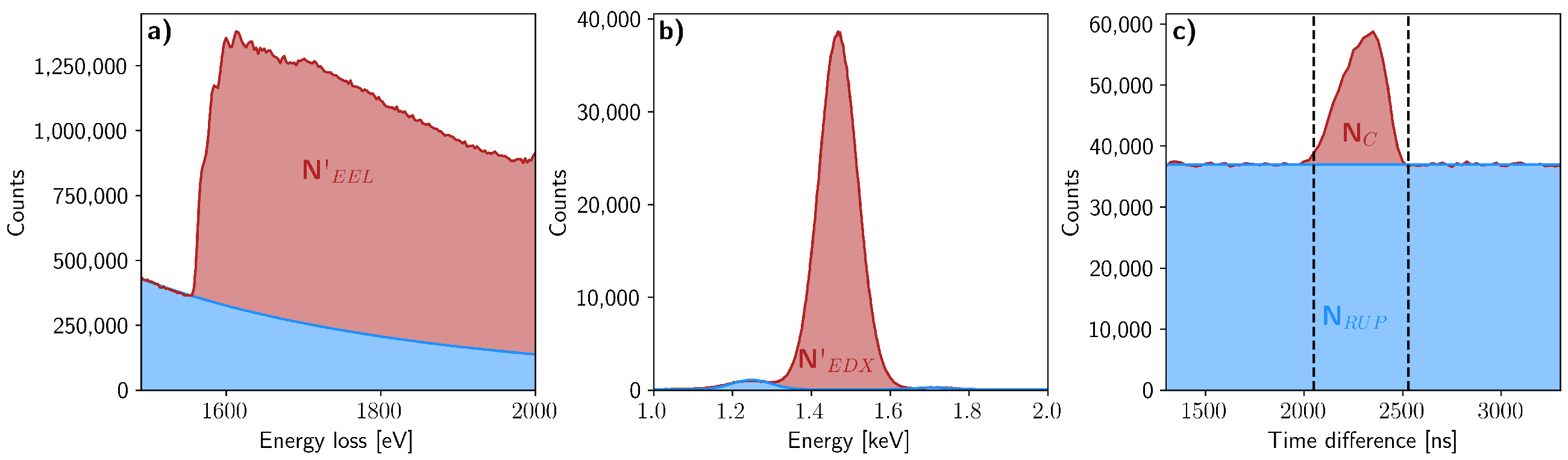
This method was used to determine the collection efficiencies of the experimental setup ( and ) used in this work using an Al-Mg-Si-Cu alloy as an example [22]. In Figure 1a, the conventional EEL spectrum is shown where is standardly determined by subtracting the background events from the signal where the background is determined by fitting a power law before the edge onset. (see Figure 1b) is determined by fitting the EDX spectrum with the sum of three Gaussian and a linear slope where one Gaussian contains the characteristic aluminum peak. The other characteristic peaks come from low-concentration copper and silicon. Finally, is calculated by first determining the time coincidence interval which is indicated in Figure 1c which shows the histogram of time difference between the X-ray and electron events. This histogram is similar to the second order correlation g which is used to measure the photon bunching [23] and antibunching [24,25]. The next step is to determine which is done by taking the average counts outside the coincidence window and multiplying this with the time coincidence window. is then calculated by subtracting the total number of events inside the time coincidence window by . Using the three values shown in Figure 1, the collection efficiencies can be determined. The two collection efficiencies are and . For , a value between 20–50% is expected [19] and for a value of 5.2% is predicted [26]. Compared to the standard methods which are used to determine the collection efficiencies for EELS and EDX, this method has the benefit that no reference sample is required, and knowledge of the beam current is not needed [21] but the ratio (/) should be known which can be computed theoretically.
4.2. Influence of Beam Current
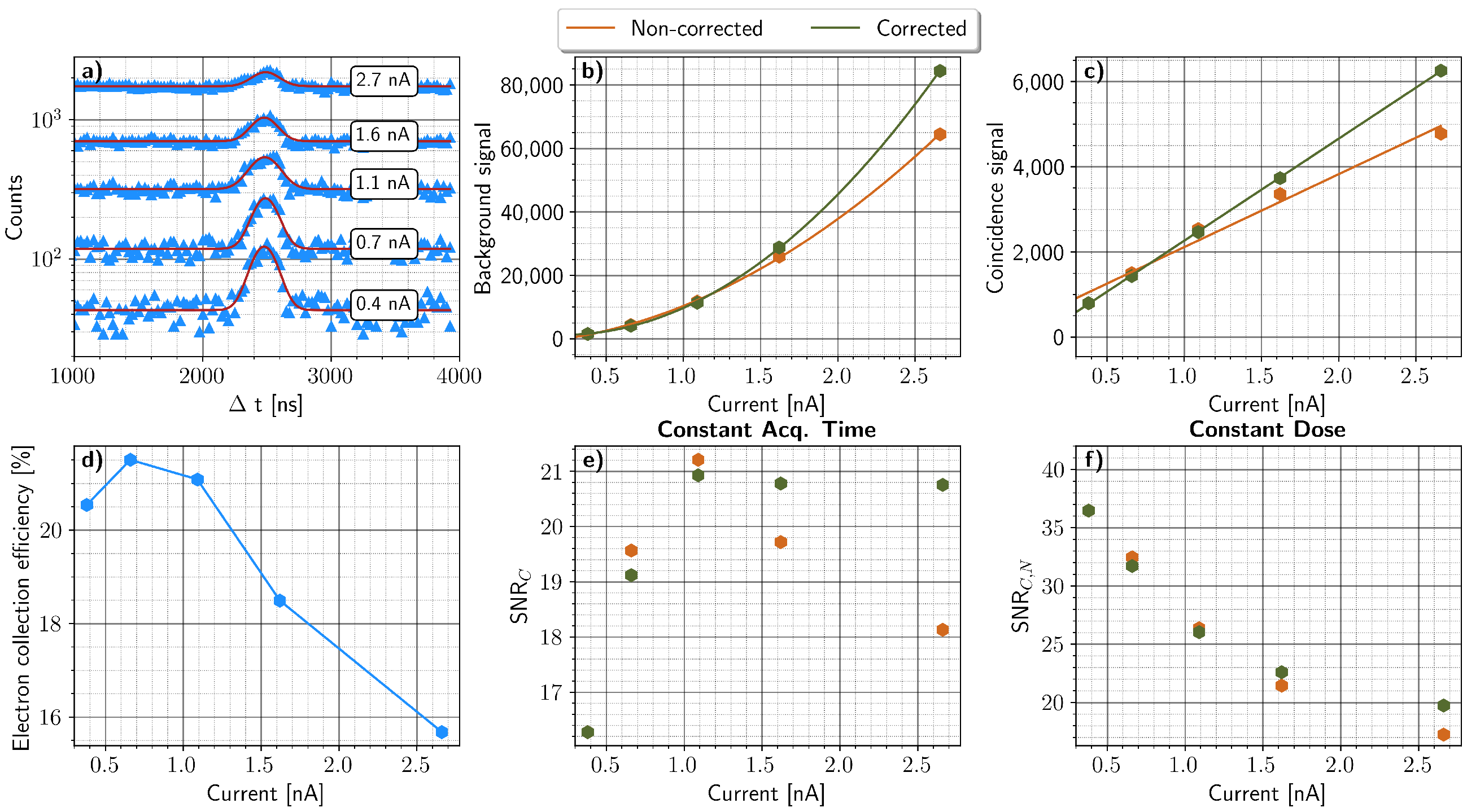
To validate Equations (3) and (4), coincidence measurements have been performed at five different incoming beam currents I on a silicon K-edge in a silicon reference sample. The beam current is measured using the current meter which is connected to the fluorescent screen of the microscope. In Figure 2a, the different time coincidence histograms are shown where the RUP is the constant background, and the peak reveals the actual coincidence events. The acquisition time is kept constant, and the incoming electron current is varied. Please note that the center of the coincidence window is around 2500 ns which is not due to the lifetime of the atom itself since this is multiple orders of magnitude faster. The offset is due to the analog filter that we used for the synchronization. Fortunately, this only gives a constant offset which is of no importance for the coincidence method.
Using the method explained in Section 4.1 we extract the and . In Figure 2b,c and are plotted as a function of beam current and labeled as non-corrected. By inspecting Figure 2c some deviation from the fitted linear curve is seen. The origin of this discrepancy is that the electron detection efficiency () depends on the beam current which is shown in Figure 2d. This can be explained by the fact that every individual pixel has a certain dead time during which it cannot detect a new event. Hence when the count rate increases, more events are lost since they arrive inside this dead time interval. The method for collection efficiency determination was used to extract at the different incoming beam currents. The values obtained for the efficiency are used to correct the observed and and in Figure 2b,c the corrected values are shown which better approximate the expected linear and quadratic dependencies. Even when current reading from the current meter has a limited precision, the data shows a clear linear and quadratic trend. From the information on and , the SNR can be calculated using Equation (5) as shown in Figure 2e which theoretically should increase with increasing current (Equation (7)). The non-corrected curve shows a decrease in SNR which is due to the loss of at higher currents indicating that Equation (7) only holds when the efficiency stays constant as a function of incoming current which for the electron detector used here is not the case. The validity of Equation (7) can still be investigated by incorporating the measured electron efficiency into the SNR which is shown in Figure 2e (green) where an increase with current is observed. The validation of Equation (8) is performed by varying the acquisition time such that the product of time and current is constant. The resulting is shown in Figure 2f where, as expected, a decrease of SNR is observed with increasing current implying that when having a fixed dose, the lower the current, the higher the SNR at the expense of acquisition time. Please note that this is in strong contrast with conventional EELS or EDX where the SNR depends only on the total dose.
4.3. EELS Background Subtraction
Contrary to conventional EELS, no prior knowledge of the background signal is needed since the RUP events contain all the information of the background. Indeed the signal is independent of the time difference between the X-rays and electrons and hence the background signal is approximated very well using all events outside the time coincidence interval [8,11].
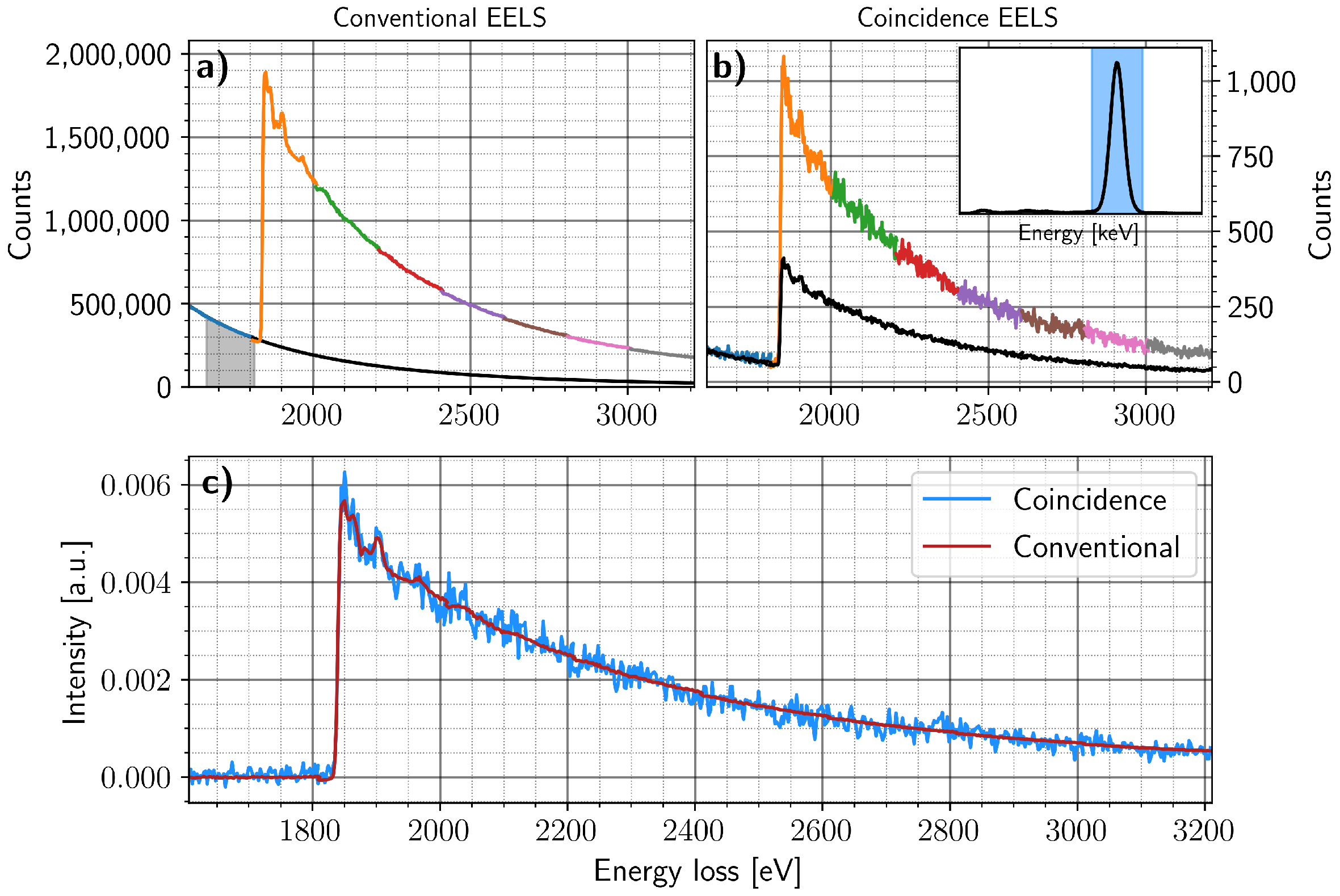
In previous works, a proof of principle was shown but a clear experimental validation with respect to conventional background subtraction was lacking. Therefore, in the present work, eight coincidence datasets were recorded where for each set we shift the energy range of the EELS detector by 200 eV. This provides eight experimental EELS spectra with consecutive energy windows. The incoming current and acquisition time was kept constant over all measurements. The core-loss edge measured is the K-edge from Si on a crystalline Si reference sample. In Figure 3a, the combined EEL spectrum is given, where each color indicates a different acquisition and energy window. The black line indicates the fitted background signal which is obtained via power-law fitting where the grey area indicates the fitting region [19]. The background fitting was performed using the Hyperspy open-source software [27]. Figure 3b shows the coincidence EEL spectrum with considerably more noise due to the fact that only a small subset of the EELS events is retained as coincident events (∼0.1%). This can be explained by comparing Equations (1) and (3) where the number of coincident events is a factor of smaller than where and [28]. The background signal (black) is obtained by taking only electrons which do not have an X-ray within the time coincidence interval region ranging from 2200–2600 ns which is chosen to include all the coincidence events inside the interval. Please note that the background signal also includes some edge signal since there are uncorrelated events arising from the inelastic scattering on the Si K-edge (see Equation (4)). In Figure 3c, the conventional and coincidence background-subtracted EEL spectra are scaled and shown together for comparison. The coincidence method reproduces the result obtained from the standard power-law subtraction method where no significant discrepancy between the two signals is observed. The noise on the coincidence EEL spectrum is considerably larger as the number of detected coincidence events is only 0.1% compared to the number of detected EEL electrons. At first sight it therefore seems that coincidence background subtraction only leads to the same result with higher noise.
The advantage of the coincidence EEL spectra, however, is that no pre-edge region was needed to subtract the background. This is of fundamental importance when, e.g., core-loss energies of two elements are close to each other preventing a good background fitting region in conventional EELS [29]. This situation also occurs often in the low loss regime, but in this case correlation with cathodoluminescence photons would be required as opposed to the X-rays used here, which would form a highly attractive area for future research as well [30].
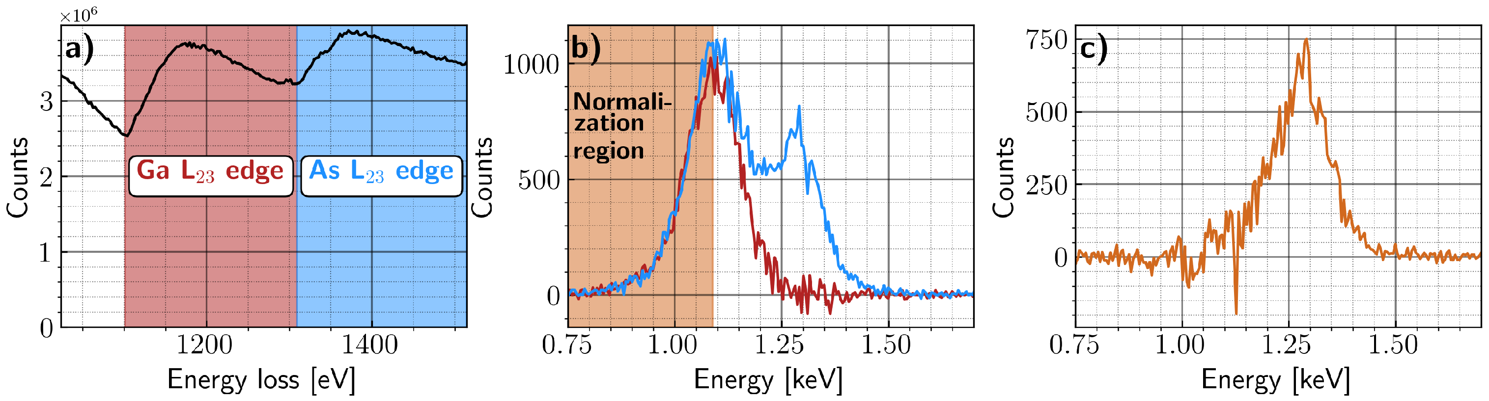
Even when X-ray lines are overlapping due to the limited energy resolution of the detectors, the EEL background signal can be correctly subtracted which is shown in Figure 4. In Figure 4a the X-ray spectrum of GaAs semiconductor reference sample is shown, the red and blue line indicate the extent of respectively the Ga L line and As L line. It is clear that by selecting regions 1+2 in Figure 4a X-rays arising from both the As and Ga atoms are included when creating the background-subtracted EEL signal, which is shown in Figure 4b. An additional shoulder in the EEL spectrum is visible coming from electrons that scattered inelastically with the As L23 edge. To remove the electron from the As signal only X-rays with energy in region 1 are chosen. The same principle can be used to remove the inelastic Ga L23 electrons from the As L23 edge. This is shown in Figure 4d where the spectrum from region 2 only contains As L23 edge electrons. The disadvantage from this method is that a sub selection within the X-ray energy window is chosen which gives fewer events, hence increasing the noise. The noise will even increase more if the X-ray lines lie closer in energy since there will only be a small window where only one X-ray line will be present.
4.4. EDX Background Subtraction
The methodology used for background-free EELS can also be applied to EDX spectra. Although the presence of a background signal in EDX is quite limited, there is an issue when due to the poor energy resolution, different peaks start overlapping. The standard method to disentangle these peaks is to use a deconvolution method [21,31,32]. However, with this method caution should be taken since artefacts can arise [32]. The coincidence method gives the ability to subtract other X-ray lines by selecting a particular EEL energy window and creating the X-ray spectrum using X-rays inside and outside the time coincidence window. In Figure 5a, the conventional EEL spectrum from a GaAs semiconductor is shown where the different edges are indicated. In Figure 5b, the background-subtracted EDX spectra are shown where the electron energies are indicated on (a). The red spectrum only uses electrons arising from the Ga L23 edge which makes that only the X-rays originating from Ga are visible. When taking electrons with energies inside the blue region, both X-ray lines are seen. This is because the EEL edges are delocalized which makes that in this energy-loss region electrons arising from both the interaction with Ga and As are located. A method to disentangle the As L from the Ga L spectrum is to normalize both spectra from Figure 5 in the region where only the Ga L X-rays are present. Then the coincidence X-ray spectrum, with both electrons coming from Ga and As, is subtracted with the coincidence X-ray spectrum where only the Ga electrons are present resulting in an X-ray spectrum containing only X-rays from the As L line. Another advantage of the coincidence method compared to conventional EDX is that it removes the phosphorescent X-rays since the energy loss of the correlated electron does not correspond to the expected edge. This improves the accuracy of the quantification and further investigation needs to be done to confirm this hypothesis.
4.5. Low Concentration Detection
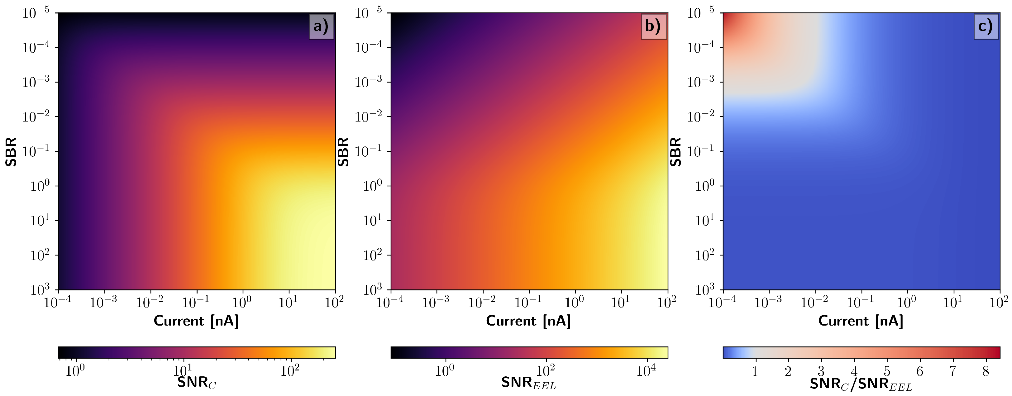
In this section, when the coincidence method can have advantages compared to conventional EELS and EDX is investigated. This is done by comparing the SNR between coincidence and conventional EELS/EDX which is calculated using Equations (A1) and (A2). The two main parameters which define the SNR are the incoming current I and signal-to-background ratio () which for EELS is defined as . Similarly for EDX, the is defined as . The other parameters chosen for the calculations are shown in Table A1 where the value for C is approximated using Equation (1) on experimental data from which and B are the values obtained from Section 4.1, I is measured from the read out of fluorescence screen and time t is acquisition time. All these values are plugged into Equations (6) and (A1) while varying I and . The formula for calculating the SNR for EELS and EDX are given in Appendix A. In Figure 6a,b both and are shown where the acquisition time has been kept constant for every calculation. An increase in SNR is seen when the incoming current and increases, as could be expected. To verify under which circumstances coincidence detection outperforms conventional EELS, the ratio is shown in Figure 6c. This shows that there is a well-defined parameter space for which coincidence detection outperforms conventional EELS, more specifically in the low current and low regime. The same analysis can be applied for EDX since the main difference for the SNR is the fluorescence yield (see Equation (A2)). Hence similar conclusions can be obtained albeit that typically for EDX the is significantly higher than for EELS explaining why it is commonly accepted that EDX is preferable when it comes to trace element detection even though the detection efficiency is considerably lower than for EELS [33]. Please note that this derivation takes only Poisson noise statistics into account and assumes an ideal detector and perfect background subtraction with no extrapolation and fitting error [34,35,36,37]. From Figure 6c one can conclude that also with conventional EELS we can detect low-concentration species in a surrounding matrix (low SBR situation) by choosing the current high enough. In practice, beam damage and limitations on total exposure time due to drift will limit the maximum dose.
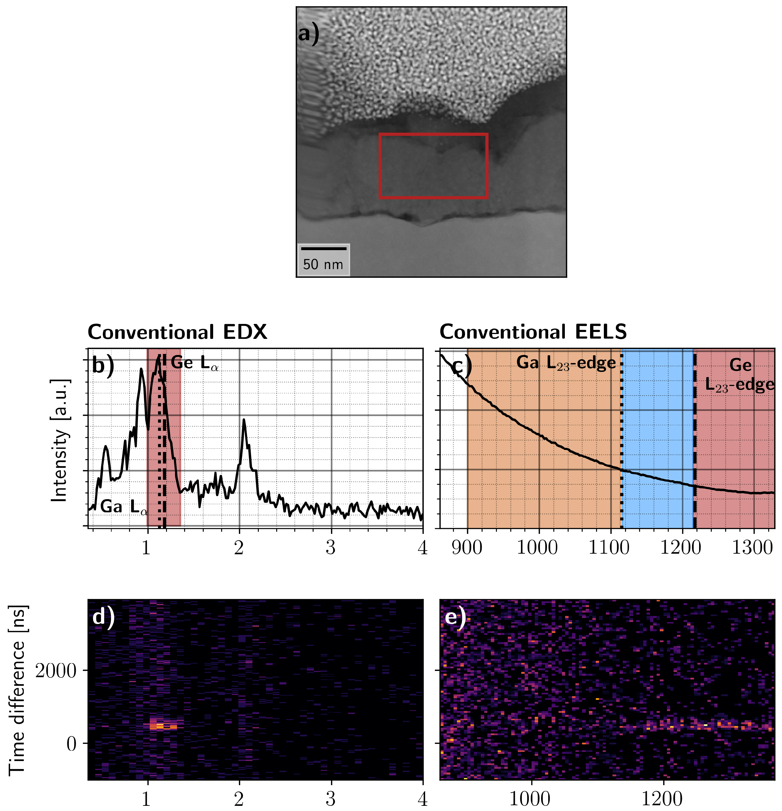
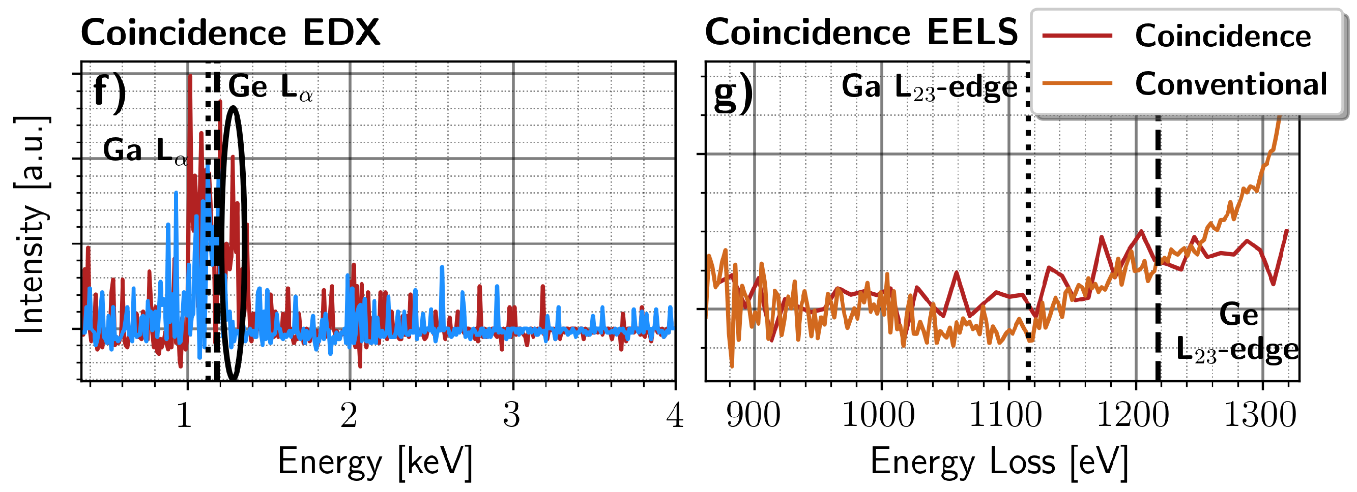
To demonstrate the above prediction, a coincidence mapping on a 100 nm layer of diamond, grown on top of a germanium substrate, was performed using a 300 × 1024 × 1024 scan with a dwell time of 10 s. The sample drift per frame was calculated using the individual EELS frames since they have sufficient signal per frame to align them. The drift-corrected and summed EELS signal is shown in Figure 7a where the distortions on the left are flyback distortions since there was no flyback time in the experimental setup. For this sample, the main inquiry was to measure if there was any Ge incorporated in the diamond layer. The first step is to create an average EEL and EDX spectrum in a region of the diamond layer where the region of interest is shown in Figure 7a. The conventional EDX and EELS spectra are shown in Figure 7b,c. The conventional EDX spectrum shows an X-ray peak at the energy of Ge where the overlap of another X-ray peak, originating from the Cu L X-ray line, of the experimental sample grid [21]. Furthermore, due to the FIB sample preparation method Ga is likely incorporated into the sample which has a similar core-loss energy making it hard to distinguish between the Ge and Ga for EDX. The conventional EELS spectrum does not show any features around the Ge L-edge, or Ga L-edge. However, when fitting a power law to the background region indicated in Figure 7g, a small gradual increase is seen starting from the Ga L-edge which does not correspond to a sharp core-loss edge. The gradual increase of the background-subtracted signal gives no clear indication on the presence of Ga or Ge. The residual spectrum seen from the background fit comes from the incapacity of the power law to reproduce the background signal when the abundance of the element is very low. Next, the two-dimensional histogram using time difference and X-ray energy is shown in Figure 7d where the post selection electron energy-loss window is shown in Figure 7c (red window). An increase in signal is observed inside the time coincidence interval at a particular X-ray energy. From the two-dimensional histogram, the coincidence and background signal is calculated as discussed in Section 4.3. From this two background-free EDX spectra are calculated where the colors correspond to the EELS energy windows shown in Figure 7c (blue and red). The blue window only corresponds to electrons undergoing the core-loss events with Ga. The red window has both Ga and Ge electrons in the coincidence signal hence both X-ray lines are excited which is similar to Figure 5. This is seen in Figure 7f where for the red spectrum, a small increase in signal is seen at higher energies indicating the presence of X-rays with a larger energy (see black ellipse) than the one arising from the Ga L line. The same method can be applied for EELS where in Figure 7e the 2D histogram between time difference and EEL energy is shown. An increase in signal at higher electron energy loss is seen inside the time coincidence window indicating the presence of an element with a core-loss edge at these energy ranges. The background-subtracted coincidence EEL signal is shown in Figure 7g where an onset is seen at an energy around 1100 eV which is before the Ge L-edge but could correspond to the Ga L-edge (1115 eV). However, slower onset on the edge signal and the occurrence of higher X-ray energies when increasing the electron energy-loss indicates the presence of an element with a larger edge and X-ray energy hence the origin could be due to Ge. Please note that the coincidence EEL spectrum is binned to improve the SNR of the spectrum.
This experimental data shows the advantage of the coincidence setup where in conventional EELS no presence of any core-loss edge is seen. When looking at the X-ray spectrum, a peak where Ge is expected is seen, and the Cu X-ray line also makes the background subtraction harder. Due to the limited energy resolution of EDX no clear distinction between Ge and Ga can be made, inviting interpretation errors when Ga would not be considered. The use of EELS which has an energy resolution in the order of eV adds extra information to disentangle between the two elements and gives some evidence on the presence of Ge in this specific diamond. However, to clearly confirm the presence of Ge more experiments should be performed but this is outside the scope of this work where the aim is to show the potential of coincidence spectroscopy to reveal EELS edges which would remain hidden in conventional EELS.
4.6. Limit on the Time Resolution
Equation (5) indicates that the SNR can be decreased via multiple routes. First, as shown in Section 3 by increasing the incoming current, the SNR is improved. However, it is not always possible to increase the current due to limits of the electron gun or the sample being radiation sensitive. Another method would be to acquire longer however this is sometimes not possible due to drift which leaves us with two other options: increasing the collection efficiency or improving the time resolution of the setup. From Figure 2a it is seen that the time coincidence interval has a width of approximately 400 ns which is disappointingly low in comparison to the <10 ns sampling capabilities of both EDX and EELS detector electronics. To improve the time resolution, the contributions from the different parts of the setup should be investigated.
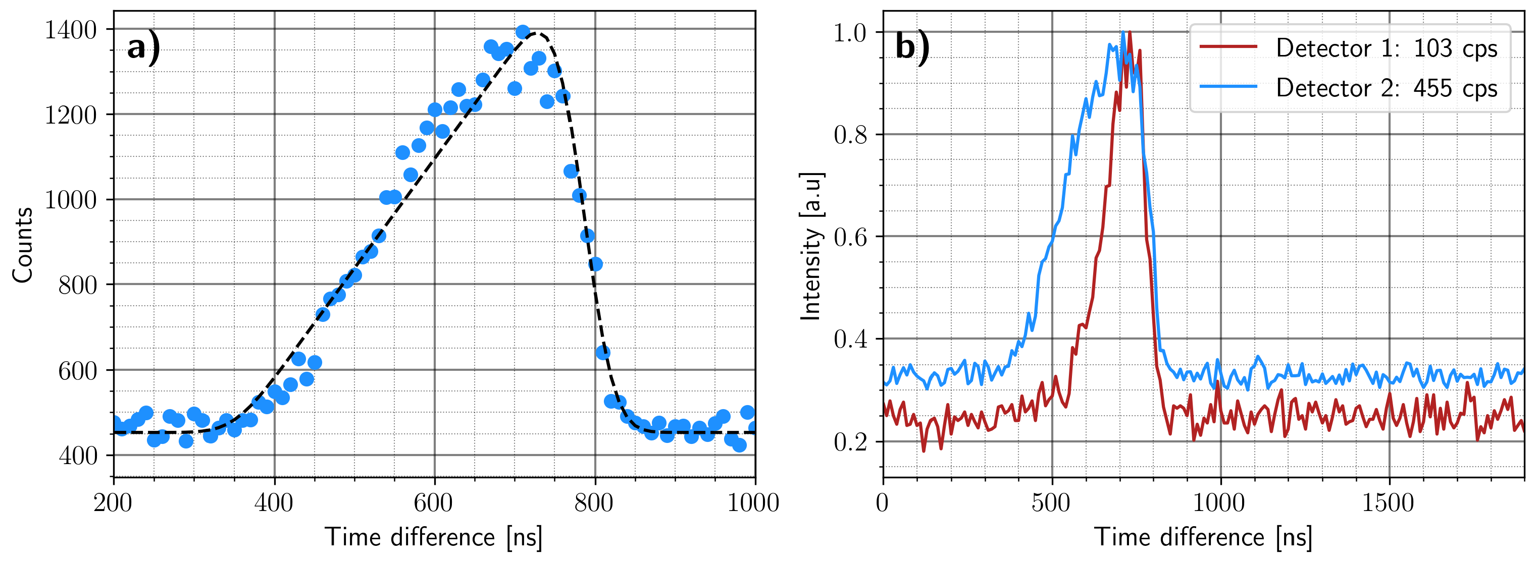
It is known that the relatively large size of the SDD detectors influences the TOA of the X-rays. This is of no surprise since the SDD was developed as a 2D position-sensitive detector for ionizing particles where the point of impact was derived using the travel time of the signal [38,39]. If the limiting factor on the time resolution would be the area of the detectors then this would be visible in the shape of the time coincidence interval. The X-ray detectors used in the experiment have a circular shape, which should correspond to a sawtooth shape for the time resolution since the travel time depends linearly on the distance between X-ray impact point and detector center but the detection area scales as meaning that on average more events will hit the outer region of the detector resulting in more weight for the longer time delays. This reasoning holds when the detector normal points exactly on the illuminated area on the sample. When this is not the case, the probability for an X-ray to land on the detector area is non-homogeneous modifying time coincidence histogram. However due to the configuration of the detector setup, this is expected to be a minor effect, but more research needs to be performed to understand this influence. In Figure 8a, the time coincidence histogram is shown from which an asymmetric shape is indeed visible (blue). The black dotted line is a sawtooth function convolved with an extra instrumental Gaussian function with a standard deviation of 30 ns. This model shows that the shape and size of the SDD plays a dominant role in limiting the time resolution to a value much lower than what we could handle with the electronics. The extra convolution with 30 ns could be related to the finite electronic bandwidth of the preamplifier stages which would then be estimated to be in the 10 MHz range. Another time resolution limiting factor could be in the electron detector where the fast electrons interact inelastically at a stochastic depth which in combination with the finite drift velocity leads to a timing uncertainty of the electron arrival event. For a sensor thickness of 300 m and a drift velocity in the order of 10 cm/s [40] this would result in a broadening of approx 30 ns [41,42].
To verify our assumptions on the dominant role of the drift velocity in the SDD we tilt the sample holder in such a way that one detector receives a smaller count rate than the other one. This happens since the holder shadows a part of the detector hence a smaller area is illuminated. In Figure 8b, both time coincidence histograms are shown from which the X-ray count rate on the detector is indicated. The width of the coincidence window for the non-shadowed detector (blue) is around twice as high as compared to the shadowed one (red) confirming that the illuminated area plays the most important role on the time resolution for the current coincidence setup.
One way to overcome this limitation could be to design new types of X-ray detectors which are similar to the pixelated electron detector with more channels, each with an integrated preamplifier stage, with a smaller active area to improve the time resolution while maintaining a high solid angle. Highly integrated electronics could potentially make this a viable solution in the near future [43]. An alternative method could be to shadow some part of the detector where a smart choice on the masked area could improve the SNR. Since the detector is circular with radius R, we can choose a circular mask which is centered on the detector with a radius r between 0 and R. The efficiency () and time resolution () of the new masked detector is:
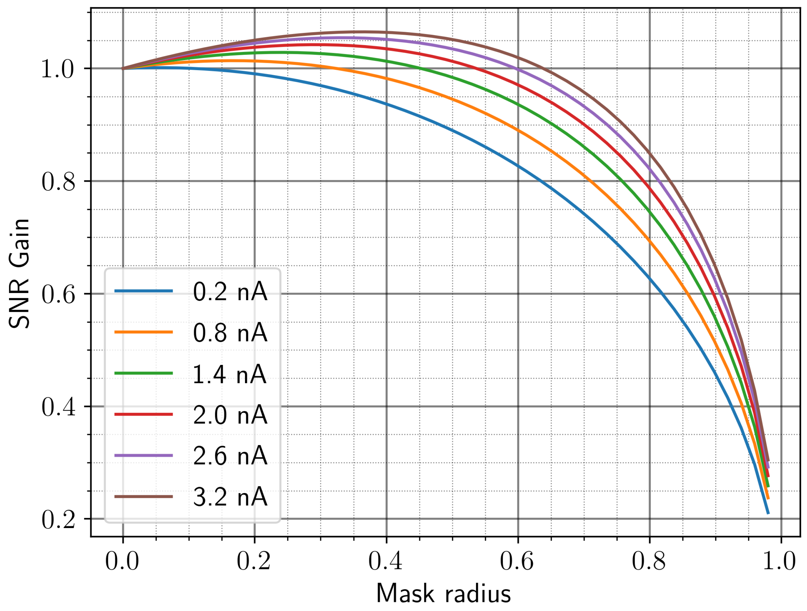
where is the broadening which arises from other time broadening influences in the experimental setup. These equations were derived for a geometry in which the detector is not tilted with respect to the sample. For tilted detectors, the situation would be different. By inserting the two values into Equation (5) the influence on the radius of the mask on the SNR can be investigated. To do this, values on the other parameters should be known. Here the values are approximated from the data shown in Figure 2. The parameter values used for the SNR simulation in Figure 9 are shown in Table A2. Please note that some parameters values given relative to , for instance which indicates that the number of background electrons is equal to the number of electrons in the core-loss edge. In Figure 9, the SNR gain, defined as the ratio of the SNR with the SNR when the mask radius is zero, as a function of mask radius for different incoming electron currents is shown. The gain in SNR is maximal when the current is higher and has an increase of 7%. Further with higher current, the optimal mask radius increases to 0.37 for the highest current used. From these calculations it is seen that the detector masking using an annular detector can increase the SNR at the expense of detection efficiency. However, the gain provided by this trick is minor and depends on the incoming current hence making this option not very attractive.
It should be noted that improving the time resolution by a factor 10–100 should be technically feasible which would result in an equal reduction in required dose for the same SNR and hence is the single most important parameter to improve when trace element analysis is required through coincidence measurement.
5. Conclusions and Outlook
In this work, a novel setup is demonstrated which can record the time of arrival of individual X-rays and inelastically scattered electrons with nanosecond precision.
The advantage of this method is that it reveals correlation data while preserving the full EELS and EDX signal without compromise in speed or acquisition time. We demonstrate that the correlation information provides several important advantages on top of simply merging two independent spectral channels. Model-free background subtraction takes away the requirement of having to fit a model background in a fitting region and is especially interesting in cases where overlapping edges occur. We show that coincidence detection provides a benefit for low-concentration elements in the presence of a high background as would occur in cases relating to doping and trace elements; typically, topics which are hard or even impossible to treat with EELS despite its very favorable detection efficiency.
We identified the single most important parameter to further improve detection limits in coincidence detection between core-loss EELS and EDX to be the limited time resolution due to large area SDD detectors that are commonly used in modern TEM setups. The most optimal way to make progress here would be to redesign the EDX detectors with the requirement of both high collection efficiency and good time resolution. We estimate that another factor 10–100 could be achievable which would have a similar effect as improving the electron dose by that same factor without the downside of beam damage or drift.
The novel method of detecting single events instead of the integrated signal, opens up possibilities for other types of scattering phenomena where signals are correlated with each other in time such as EELS-CL, secondary electrons-EELS and many more. The intrinsic data compression by storing only actual events, the lack of readout time and the fact that synchronization between multiple detectors is reduced to the problem of syncing them all to a single master clock holds many benefits for implementation in TEM setups with their ever-increasing number of detectors and datarates.
Author Contributions
Conceptualization, J.V. and K.M.-C.; Development experimental setup, D.J., A.B., K.M.-C. and J.V.; Experimental data acquisition, D.J.; Data analysis, D.J.; writing-original draft preparation, D.J.; writing-review and editing, A.B., K.M.-C. and J.V. All authors have read and agreed to the published version of the manuscript.
Funding
This project has received funding from the European Union’s Horizon 2020 research and innovation program under grant agreement No 823717 ESTEEM3. J.V., K.M.-C. and D.J. acknowledge funding from FWO project G042920N ‘Coincident event detection for advanced spectroscopy in transmission electron microscopy’. We acknowledge funding under the European Union’s Horizon 2020 research and innovation program (J.V. and D.J. under grant agreement No 101017720, FET-Proactive EBEAM). K.M.-C. acknowledges funding from the Helmholtz society under contract VH-NG-1317.
Data Availability Statement
The full datasets and software are made available on Zenodo [18].
Acknowledgments
The authors would like to express their gratitude to M. Tence for significant help with scan engine, to M. Kociak for fruitful discussions, to F. Houdelier for help with video port on Gatan imaging filter and K. Haenen of the University of Hasselt for providing the diamond test sample.
Conflicts of Interest
The authors declare no conflict of interest.
Appendix A. Signal-to-Noise for EELS and EDX
Appendix B. Parameters Low Concentration Detection

Table A1.
The values for the parameters used in the calculation of comparison of and .
| C | C | [ns] | ||||
|---|---|---|---|---|---|---|
| 3.75 × 10 | 3C | 0.2 | 0.05 | 400 | 0.042 | 0.05 C |
Appendix C. Parameters Masking Detector Area
Table A2.
The values for the parameters used in the calculation of SNR when masking the detector.
| C | C | [ns] | [ns] | |||||
|---|---|---|---|---|---|---|---|---|
| 3.75 × 10 | 3C | 0.2 | 0.05 | 400 | 30 | 0.042 | C | 0.05 C |
References
- Bolić, M.; Drndarević, V. Digital gamma-ray spectroscopy based on FPGA technology. Nucl. Instrum. Methods Phys. Res. Sect. A 2002, 482, 761–766. [Google Scholar] [CrossRef]
- Arnold, L.; Baumann, R.; Chambit, E.; Filliger, M.; Fuchs, C.; Kieber, C.; Klein, D.; Medina, P.; Parisel, C.; Richer, M.; et al. TNT digital pulse processor. IEEE Trans. Nucl. Sci. 2006, 53, 723–728. [Google Scholar] [CrossRef]
- Papp, T.; Maxwell, J. A robust digital signal processor: Determining the true input rate. Nucl. Instrum. Methods Phys. Res. Sect. A 2010, 619, 89–93. [Google Scholar] [CrossRef]
- Akiba, K.; Artuso, M.; Badman, R.; Borgia, A.; Bates, R.; Bayer, F.; van Beuzekom, M.; Buytaert, J.; Cabruja, E.; Campbell, M.; et al. Charged particle tracking with the Timepix ASIC. Nucl. Instrum. Methods Phys. Res. Sect. A 2012, 661, 31–49. [Google Scholar] [CrossRef] [Green Version]
- Ballabriga, R.; Campbell, M.; Llopart, X. Asic developments for radiation imaging applications: The medipix and timepix family. Nucl. Instrum. Methods Phys. Res. Sect. A 2018, 878, 10–23. [Google Scholar] [CrossRef] [Green Version]
- Drescher, M.; Hentschel, M.; Kienberger, R.; Uiberacker, M.; Yakovlev, V.; Scrinzi, A.; Westerwalbesloh, T.; Kleineberg, U.; Heinzmann, U.; Krausz, F. Time-resolved atomic inner-shell spectroscopy. Nature 2002, 419, 803–807. [Google Scholar] [CrossRef]
- Nicolas, C.; Miron, C. Lifetime broadening of core-excited and -ionized states. J. Electron Spectrosc. Related Phenom. 2012, 185, 267–272. [Google Scholar] [CrossRef]
- Kruit, P.; Shuman, H.; Somlyo, A. Detection of X-rays and electron energy loss events in time coincidence. Ultramicroscopy 1984, 13, 205–213. [Google Scholar] [CrossRef]
- Oelsner, A.; Schmidt, O.; Schicketanz, M.; Klais, M.; Schönhense, G.; Mergel, V.; Jagutzki, O.; Schmidt-Böcking, H. Microspectroscopy and imaging using a delay line detector in time-of-flight photoemission microscopy. Rev. Sci. Instrum. 2001, 72, 3968–3974. [Google Scholar] [CrossRef]
- Müller-Caspary, K.; Oelsner, A.; Potapov, P. Two-dimensional strain mapping in semiconductors by nano-beam electron diffraction employing a delay-line detector. Appl. Phys. Lett. 2015, 107, 072110. [Google Scholar] [CrossRef]
- Jannis, D.; Müller-Caspary, K.; Béché, A.; Oelsner, A.; Verbeeck, J. Spectroscopic coincidence experiments in transmission electron microscopy. Appl. Phys. Lett. 2019, 114, 143101. [Google Scholar] [CrossRef] [Green Version]
- Gromov, V. Development and applications of the Timepix3 chip. In Proceedings of the 20th Anniversary International Workshop on Vertex Detectors—PoS(Vertex 2011), Lake Neusiedl, Austria, 19–24 June 2011; p. 46. [Google Scholar] [CrossRef]
- Zobelli, A.; Woo, S.Y.; Tararan, A.; Tizei, L.H.; Brun, N.; Li, X.; Stéphan, O.; Kociak, M.; Tencé, M. Spatial and Spectral Dynamics in STEM Hyperspectral Imaging Using Random Scan Patterns. Ultramicroscopy 2019, 212, 112912. [Google Scholar] [CrossRef] [Green Version]
- Harrach, H.S.v.; Dona, P.; Freitag, B.; Soltau, H.; Niculae, A.; Rohde, M. An integrated multiple silicon drift detector system for transmission electron microscopes. J. Phys. Conf. Ser. 2010, 241, 012015. [Google Scholar] [CrossRef]
- Bombelli, L.; Manotti, M.; Altissimo, M.; Kourousias, G.; Alberti, R.; Gianoncelli, A. Towards on-the-fly X-ray fluorescence mapping in the soft X-ray regime. X-ray Spectrom. 2019, 48, 325–329. [Google Scholar] [CrossRef]
- Jannis, D.; Hofer, C.; Gao, C.; Xie, X.; Béché, A.; Pennycook, T.J.; Verbeeck, J. Event Driven 4D STEM Acquisition with a Timepix3 Detector: Microsecond Dwell Time and Faster Scans for High Precision and Low Dose Applications. arXiv 2021, arXiv:2107.02864. [Google Scholar]
- Savitzky, B.H.; El Baggari, I.; Clement, C.B.; Waite, E.; Goodge, B.H.; Baek, D.J.; Sheckelton, J.P.; Pasco, C.; Nair, H.; Schreiber, N.J.; et al. Image registration of low signal-to-noise cryo-STEM data. Ultramicroscopy 2018, 191, 56–65. [Google Scholar] [CrossRef] [Green Version]
- Jannis, D.; Müller-Caspary, K.; Béché, A.; Verbeeck, J. Coincidence Detection of EELS and EDX Spectral Events in the Electron Microscope. Zenodo 2021. [Google Scholar] [CrossRef]
- Egerton, R.F. Electron Energy-Loss Spectroscopy in the Electron Microscope, 3rd ed.; Springer: Berlin, Germany, 2011. [Google Scholar]
- Zemyan, S.M.; Williams, D.B. Standard performance criteria for analytical electron microscopy. J. Microsc. 1994, 174, 1–14. [Google Scholar] [CrossRef]
- Williams, D.B.; Carter, C.B. Transmission Electron Microscopy: A Textbook for Materials Science, 2nd ed.; Springer: Berlin, Germany, 2009. [Google Scholar]
- Ding, L.; Jia, Z.; Nie, J.F.; Weng, Y.; Cao, L.; Chen, H.; Wu, X.; Liu, Q. The structural and compositional evolution of precipitates in Al-Mg-Si-Cu alloy. Acta Mater. 2018, 145, 437–450. [Google Scholar] [CrossRef]
- Brown, R.H.; Twiss, R. LXXIV. A new type of interferometer for use in radio astronomy. Lond. Edinb. Dublin Philos. Mag. J. Sci. 1954, 45, 663–682. [Google Scholar] [CrossRef]
- Chandra, N.; Prakash, H. Anticorrelation in Two-Photon Attenuated Laser Beam. Phys. Rev. A 1970, 1, 1696–1698. [Google Scholar] [CrossRef]
- Paul, H. Photon antibunching. Rev. Mod. Phys. 1982, 54, 1061–1102. [Google Scholar] [CrossRef]
- Kraxner, J.; Schäfer, M.; Röschel, O.; Kothleitner, G.; Haberfehlner, G.; Paller, M.; Grogger, W. Quantitative EDXS: Influence of geometry on a four detector system. Ultramicroscopy 2017, 172, 30–39. [Google Scholar] [CrossRef]
- de la Pena, F.; Prestat, E.; Fauske, V.T.; Burdet, P.; Jokubauskas, P.; Nord, M.; Ostasevicius, T.; MacArthur, K.E.; Sarahan, M.; Johnstone, D.N.; et al. Hyperspy/Hyperspy: HyperSpy v1.5.2. Zenodo 2019. [Google Scholar] [CrossRef]
- Campbell, J.L.; Cauchon, G.; Lakatos, T.; Lépy, M.C.; McDonald, L.; Papp, T.; Plagnard, J.; Stemmler, P.; Teesdale, W.J. Experimental K-shell fluorescence yield of silicon. J. Phys. B At. Mol. Opt. Phys. 1998, 31, 4765–4779. [Google Scholar] [CrossRef]
- Tenailleau, H.; Martin, J.M. A new background subtraction for low-energy EELS core edges. J. Microsc. 1992, 166, 297–306. [Google Scholar] [CrossRef]
- Graham, R.J.; Spence, J.; Alexander, H. Infrared Cathodoluminescence Studies from Dislocations in Silicon in tem, a Fourier Transform Spectrometer for Cl in Tem and Els/cl Coincidence Measurements of Lifetimes in Semiconductors. MRS Proc. 1986, 82, 235. [Google Scholar] [CrossRef]
- Ingamells, C.O.; Fox, J.J. Deconvolution of energy-dispersive X-ray peaks using the poisson probability function. X-ray Spectrom. 1979, 8, 79–84. [Google Scholar] [CrossRef]
- Brodusch, N.; Zaghib, K.; Gauvin, R. Improvement of the energy resolution of energy dispersive spectrometers (EDS) using Richardson–Lucy deconvolution. Ultramicroscopy 2020, 209, 112886. [Google Scholar] [CrossRef]
- Shuman, H.; Somlyo, A. Electron energy loss analysis of near-trace-element concentrations of calcium. Ultramicroscopy 1987, 21, 23–32. [Google Scholar] [CrossRef]
- Egerton, R. A revised expression for signal/noise ratio in EELS. Ultramicroscopy 1982, 9, 387–390. [Google Scholar] [CrossRef]
- Hofer, F.; Grogger, W.; Kothleitner, G.; Warbichler, P. Quantitative analysis of EFTEM elemental distribution images. Ultramicroscopy 1997, 67, 83–103. [Google Scholar] [CrossRef]
- Egerton, R.; Malac, M. Improved background-fitting algorithms for ionization edges in electron energy-loss spectra. Ultramicroscopy 2002, 92, 47–56. [Google Scholar] [CrossRef]
- Fung, K.L.; Fay, M.W.; Collins, S.M.; Kepaptsoglou, D.M.; Skowron, S.T.; Ramasse, Q.M.; Khlobystov, A.N. Accurate EELS background subtraction—An adaptable method in MATLAB. Ultramicroscopy 2020, 217, 113052. [Google Scholar] [CrossRef]
- Gatti, E.; Rehak, P. Semiconductor drift chamber—An application of a novel charge transport scheme. Nucl. Instrum. Methods Phys. Res. 1984, 225, 608–614. [Google Scholar] [CrossRef] [Green Version]
- Knoll, G.F. Radiation Detection and Measurement, 4th ed.; John Wiley: Hoboken, NJ, USA, 2010. [Google Scholar]
- Ottaviani, G.; Reggiani, L.; Canali, C.; Nava, F.; Alberigi-Quaranta, A. Hole drift velocity in silicon. Phys. Rev. B 1975, 12, 3318–3329. [Google Scholar] [CrossRef]
- Gao, T.; Via, C.D.; Bergmann, B.; Burian, P.; Pospisil, S. Characterisation of Timepix3 with 3D sensor. J. Inst. 2018, 13, C12021. [Google Scholar] [CrossRef] [Green Version]
- van Schayck, J.P.; van Genderen, E.; Maddox, E.; Roussel, L.; Boulanger, H.; Fröjdh, E.; Abrahams, J.P.; Peters, P.J.; Ravelli, R.B. Sub-pixel electron detection using a convolutional neural network. Ultramicroscopy 2020, 218, 113091. [Google Scholar] [CrossRef]
- Förster, A.; Brandstetter, S.; Schulze-Briese, C. Transforming X-ray detection with hybrid photon counting detectors. Phil. Trans. R. Soc. A. 2021, 377, 20180241. [Google Scholar] [CrossRef]
Figure 1.
(a) Conventional electron energy loss (EEL) spectrum where the K-edge of aluminum is shown from an Al-Mg-Si-Cu alloy. The background is subtracted using power-law fit (blue area). The background is used to determine . (b) The conventional energy dispersive X-ray (EDX) spectrum where the main peak is a characteristic peak of aluminum. The background value is determined by fitting the spectrum to the sum of three Gaussian’s and a linear slope from which one Gaussian peak is the peak of interest. (c) Histogram of the number of correlated events as a function of time difference between the X-rays and electrons. The number of identified coincidence events is indicated on the figure.

Figure 2.
(a) Coincidence histograms as a function of time delay between EELS and EDX event streams for a varying beam current at constant acquisition time (y scale logarithmic). (b) The uncorrelated background signal as a function of incoming beam current (brown). The background scales quadratically with incoming current. In green, the corrected expected background signal which would be recorded for an ideal electron detector with constant efficiency as a function of current. (c) The number of coincidence events as a function of incoming current scales only linearly with incoming current. The corrected signal taking the efficiency into account is shown (green). Please note that the corrected fit better approximates a linear function. (d) The measured electron efficiency with a notable decrease for higher currents due to dead time in the detector. (e) The SNR of the coincidence signal as a function of incoming current when using a constant acquisition time. (f) The signal-to-noise (SNR) of the coincidence signal as a function of incoming current when the total dose has been fixed.

Figure 3.
(a) Conventional EEL spectrum obtained from eight separate acquisitions in consecutive energy windows. The black line indicates the fitted background a using power law where the fitted area is indicated with the grey area. (b) The correlated EEL spectrum when using only electrons which have an Si X-ray detected within the time correlation window. In the inset figure, the X-ray spectrum is shown where the blue area indicates the energy of the X-rays selected which correspond to the X-rays from Si. The black line is the background signal obtained from using the electrons outside the time coincidence window. (c) The coincidence and conventional background-subtracted EEL spectra from which it is seen that the background subtraction method using the correlation with X-rays can reproduce the same result as using the conventional power-law subtraction method albeit at the expense of a lower count rate. Please note that for the correlated result, no assumptions on background shape and no pre-edge fitting region was required.

Figure 4.
(a) The EDX spectrum of GaAs where the Ga peak is fitted with a Gaussian to indicate the extent of the X-rays originating from the de-excitation of the Ga atom. The red and blue line indicate the extent of the X-ray lines in the energy spectrum. (b) The background-subtracted EEL spectra using the X-rays in the regions are indicated by the legend. When only using X-rays from region 1, it is seen that only the Ga L edge is selected without the As L edge (brown). When regions 1+2 are selected, electrons from both edges are seen (green). (c) The same as (a) where the X-ray regions, out which the coincidence events are chosen, have been modified. (d) The background-free EEL spectrum where, by selecting the proper X-ray window (region 2), only the As L edge is selected (brown). When regions 1+2 are selected, electrons from both edges are seen (green).

Figure 5.
(a) The conventional EEL spectrum from GaAs where the two edges are indicated. (b) The background-subtracted EDX spectra using only electrons from the two regions indicated in (a). The red spectrum only shows X-rays originating from Ga whereas the blue region shows both Ga and As since the core-loss edges are delocalized in energy. (c) The As L line can be disentangled from the Ga L line by normalizing the blue and red spectrum from (b) in the region where only Ga L X-rays are present (brown region). The difference between the normalized blue and red spectrum results in an X-ray spectrum containing only the As L X-rays.

Figure 6.
(a,b) The SNR of the coincidence and conventional EELS while varying the and I and keeping the exposure time constant. Please note that both axes are logarithmic. The other parameters used to determine the SNR are indicated in Table A1. (c) The ratio between the SNR of coincidence and conventional EELS where a value larger than one indicates the region where coincidence outperforms conventional EELS (red colored areas).

Figure 7.
(a) A 300 × 1024 × 1024 STEM scan at 10 s on a diamond layer grown on top of a germanium substrate. The image shows the total number of electrons on the EELS detector at every probe position. The red window indicates the area from which the spectra are shown. (b,c) The conventional EDX and EELS signals. (d) Two-dimensional histogram, using a post selection on electron energy losses which are shown in (c), between time difference and X-ray energy where the electron energies chosen are the ones within the red window. (e) Similar to (d) except that one axis is now electron energy loss and the post selection is performed on the X-ray energies shown in (b). (f) The background-subtracted X-ray spectrum for the two electron energy windows indicated in (c). The black ellipse indicates the region where an excess of counts is seen compared to the blue spectrum. (g) The background-subtracted EEL spectrum where an increase of signal is observed starting from the Ga L edge indicating the presence of core-loss events. The signal is binned to improve the SNR of the spectrum. Additionally, the conventional background-subtracted EEL spectrum is shown where the region for the power-law fit is indicated in (c).


Figure 8.
(a) Zoom in on the shape of the time coincidence histogram where an asymmetric profile is seen. The dotted black line shows a Gaussian blurred sawtooth function which would be the theoretical shape of the histogram. (b) The time coincidence histogram of two detectors. The sample holder is titled such that the count rate of X-rays on detector 1 is lower which is due to the shadowing of the detector. The width of the time coincidence peak is significantly lower for the shadowed detector (detector 1).

Figure 9.
The SNR gain as function of mask radius for different incoming currents. The SNR gain is defined as the ratio of the SNR with the SNR when the mask radius is zero.
Figure 9.
The SNR gain as function of mask radius for different incoming currents. The SNR gain is defined as the ratio of the SNR with the SNR when the mask radius is zero.

Publisher’s Note: MDPI stays neutral with regard to jurisdictional claims in published maps and institutional affiliations. |
© 2021 by the authors. Licensee MDPI, Basel, Switzerland. This article is an open access article distributed under the terms and conditions of the Creative Commons Attribution (CC BY) license (https://creativecommons.org/licenses/by/4.0/).
Share and Cite
MDPI and ACS Style
Jannis, D.; Müller-Caspary, K.; Béché, A.; Verbeeck, J. Coincidence Detection of EELS and EDX Spectral Events in the Electron Microscope. Appl. Sci. 2021, 11, 9058. https://0-doi-org.brum.beds.ac.uk/10.3390/app11199058
AMA Style
Jannis D, Müller-Caspary K, Béché A, Verbeeck J. Coincidence Detection of EELS and EDX Spectral Events in the Electron Microscope. Applied Sciences. 2021; 11(19):9058. https://0-doi-org.brum.beds.ac.uk/10.3390/app11199058
Chicago/Turabian StyleJannis, Daen, Knut Müller-Caspary, Armand Béché, and Jo Verbeeck. 2021. "Coincidence Detection of EELS and EDX Spectral Events in the Electron Microscope" Applied Sciences 11, no. 19: 9058. https://0-doi-org.brum.beds.ac.uk/10.3390/app11199058
Note that from the first issue of 2016, this journal uses article numbers instead of page numbers. See further details here.