
A Dual-Band Dual-Polarized Antenna with Improved Isolation Characteristics for Polarimetric SAR Applications


1
Radar System 3rd Team, Hanwha Systems, Yongin 17121, Korea
2
Department of Electronic Engineering, Hanyang University, Seoul 04763, Korea
*
Author to whom correspondence should be addressed.
Appl. Sci. 2021, 11(21), 10025; https://0-doi-org.brum.beds.ac.uk/10.3390/app112110025
Submission received: 7 October 2021
/
Revised: 22 October 2021
/
Accepted: 25 October 2021
/
Published: 26 October 2021
(This article belongs to the Special Issue Antenna Design for Microwave and Millimeter Wave Applications II: Latest Advances and Prospects)
Abstract
:A dual-band dual-polarized antenna with high isolation characteristics is proposed for polarimetric synthetic aperture radar (PolSAR) applications. The antenna consists of four dipole antennas and 2 × 2 patch antenna arrays operating at the P-band (450–730 MHz) and Ka-band (34–36 GHz), respectively. The dipole antennas and the patch antenna arrays need dual-linear polarization characteristics to acquire PolSAR data. Improvements in the isolation characteristics at the P-band are achieved by inserting a metamaterial absorber with a fractal geometry between the transmitting (Tx) and receiving (Rx) dipole antennas. Without the absorber, the simulated isolation characteristics between the Tx and Rx antennas are lower than 19.2 dB over the target band. On the other hand, with the absorbers, the simulated isolation characteristics are higher than 23.44 dB over the target band, and remarkable improvement is achieved around the resonance frequency of the absorber. The measured results are in good agreement with the simulated ones, showing that the proposed antenna can be a good candidate for PolSAR applications.
1. Introduction
Synthetic aperture radar (SAR) is an active remote sensing system providing images of targets during day or night [1]. Since a conventional single-polarized SAR system can transmit and receive only a single-polarized signal, acquiring detailed target information for various environments is difficult. An advanced imaging radar system—i.e., a polarimetric SAR (PolSAR) system—has been proposed to overcome the limitations of the single-polarized SAR system [2,3]. The PolSAR system provides much more information about the targets than the conventional SAR system, by utilizing dual-polarized signals [2]. The PolSAR system consists of dual-polarized transmitting (Tx) and receiving (Rx) antennas. A signal that was emitted in vertical (V) polarization and received in horizontal (H) polarization would be indicated by VH. Alternatively, a signal emitted in horizontal (H) polarization and received in horizontal (H) polarization would be indicated by HH, and so on. In the PolSAR system, a single-polarized signal is transmitted from one of the Tx antennas, and two orthogonal polarized backscattered signals are collected by the Rx antennas, resulting in either VV and VH or HH and HV scattering data. VV scattering is most sensitive to the rough surface scattering caused by bare soil or water. Cross-polarized scatterings such as VH and HV are most sensitive to the volume scattering caused by leaves and branches in a forest canopy. HH scattering is most sensitive to the double-bounce scattering caused by buildings or tree trunks [3]. SAR systems operate in various frequency bands, depending on their purpose. Table 1 demonstrates commonly used frequency bands in SAR systems [3]. For example, the C-band signal can penetrate only into the top layers of the canopy of a forest. However, P-band SAR systems have much deeper penetration characteristics; therefore, underground targets can be detected. However, the images of these lower band SAR systems have low resolution. To obtain clearer images of the target, higher band SAR systems need to be utilized. For example, spatial resolutions as high as 10 cm can be achieved by Ka-band SAR systems [4]. Thus, multiband quad-pol antennas are required in order to carry out various missions with PolSAR systems. Multiband antennas were reported for SAR applications in [5,6]. In [5], the proposed antenna consists of a patch antenna and an 8 × 8 patch antenna array operating at the P-band and Ku-band, respectively; the P-band antenna has dual-linear polarization characteristics, but the Ku-band antenna has only single-linear polarization characteristics; therefore, it is not appropriate for use in PolSAR applications. In [6], dual-polarized patch antenna arrays operating at the X-band and Ku-band were proposed; although the proposed antenna is suitable for PolSAR systems due to the quad-pol characteristic, it cannot be utilized for detecting targets in forests or underground.
In this paper, a dual-band dual-polarized antenna with improved isolation characteristics is proposed for PolSAR applications. The antenna consists of Tx and Rx dipole antennas and 2 × 2 patch antenna arrays. The dipole antennas and patch antenna arrays operate at the P-band and Ka-band, respectively. Fractal-shaped metamaterial absorbers are located between the Tx and Rx antennas to enhance the isolation characteristics at the P-band.
2. Antenna Design and Performance
2.1. Single Ka-Band Patch Antenna Design and Performance
Figure 1a shows the geometry of a single patch antenna for the Ka-band. Two substrates are stacked for aperture-coupled feeding to enhance the bandwidth of the patch antenna [7]. All substrates are Rogers RT/duroid 5880 (εr = 2.2, tan δ = 0.0009). As shown in Figure 1c, a patch antenna is located on the top side of the stacked structure, and two orthogonal microstrip lines and slots are located at the bottom and middle of the structure, respectively. The detailed view of the antenna design is shown in Figure 1b. As shown in Figure 1d, dual polarization is achieved by exciting Ports 1 and 2. Figure 1e shows the simulated S-parameters of the proposed single patch antenna. The −10 dB reflection coefficient (SNN) bandwidths are 2.87 GHz (33.67–36.54 GHz) and 3.28 GHz (33–36.28 GHz) when Ports 1 and 2 are excited, respectively. The operating frequency in the Ka-band ranges from 34 to 36 GHz, and the simulated result shows that the designed antenna fully covers the target band with dual-polarization characteristics. Figure 1f,g show the simulated radiation patterns for each excitation. When Ports 1 and 2 are excited, the gains in the +z direction are 5.74 and 5.84 dBi, respectively. The front-to-back ratios (FBRs) are 28.04 and 19.29 dB with Port 1 and 2 excitations, respectively.
2.2. 2 × 2 Ka-Band Patch Antenna Array Design and Performance
In a millimeter wave band, a high gain is required in order to compensate for the high path loss caused by atmospheric absorption [8]. Therefore, we considered the antenna array in order to enhance the radiation gain in the Ka-band. Figure 2a shows the geometry of the designed 2 × 2 patch antenna array for V-pol. The center-to-center spacing of the array is 4.3 mm (0.5 λ0 at 35 GHz). As shown in Figure 2b, the simulated surface current distributions of all patch antennas have the same directions (V-pol characteristics). Figure 2c shows the simulated reflection coefficient performances of the 2 × 2 patch antenna array. The –10 dB reflection coefficient bandwidths of all ports sufficiently cover the 35 GHz target band. As shown in Figure 2d, the simulated maximum gain and FBR at 35 GHz are 10.89 dBi and 15.31 dB, respectively.
Figure 3a shows the geometry of the antenna array for H-pol. The spacing of the patch antennas is the same as that for V-pol. As shown in Figure 3b, the surface current distributions show that the antenna array has H-pol characteristics. Figure 3c shows that the simulated −10 dB reflection coefficients cover the target band. Figure 3d shows the simulated radiation pattern of the H-pol case. The simulated maximum gain and FBR at 35 GHz are 10.66 dBi and 13.28 dB, respectively.
Figure 4a,b show the antenna array with the feeding network used for fabrication. The feeding network has 180° phase-delay lines for in-phase excitation. As shown in Figure 4c, the simulated 10 dB |S11| and |S22| bandwidths are 5.43 GHz (32.77–38.2 GHz) and 5.63 GHz (31.61–37.24 GHz), respectively. In the V-pol case (Port 1 excitation), the simulated maximum gain and FBR at 35 GHz are 10.04 dBi and 5.74 dB, respectively. In the H-pol case (Port 2 excitation), the simulated maximum gain and FBR at 35 GHz are 10 dBi and 12.11 dB, respectively. Each slot aperture can be considered to be a slot antenna. Since the slot antenna radiates in both directions perpendicular to the substrate, the backlobe is mainly due to the radiation from the slot apertures. Therefore, a reflector is required to enhance the FBR performance.
Figure 5a,c show the patch antenna array with a reflector. The reflector is made of a 1.6 mm thick FR4 substrate (εr = 4.4, tan δ = 0.02) with a metal plane on the top side. As shown in Table 2, the radiation performance of the proposed antenna can be optimized by changing the gap distance (h) between the antenna and the reflector. In addition, the existence of the reflector affects the S-parameter performances, which are dependent upon the h values, as shown in Table 3. The best antenna performances considering both S-parameters and radiation performances, including maximum gain and FBR, were achieved when h was 3 mm (0.35 λ0 at 35 GHz). As shown in Figure 5d,e, the backlobe is dramatically reduced by the reflector in comparison with the results shown in Figure 4d,e.
Figure 6a shows the proposed antenna assembled by polycarbonate (PC) bolts and nuts. The gap distance is maintained by using three 1 mm thick PC plain washers. Lumped ports were used in the simulation. To investigate the effects of the RF connector and the feeding network in actual antenna measurements, simulations with the RF connectors should be carried out. A 2.92 mm end-launch connector was used in simulation [9]. As shown in Figure 6c, the simulated 10 dB |S11| and |S22| bandwidths are 4.96 GHz (33.42–38.38 GHz) and 3.44 GHz (33.08–36.52 GHz), respectively. Figure 6d,e show the simulated radiation patterns of the V- and H-pol cases. In the V-pol case, the simulated maximum gain and FBR at 35 GHz are 10.94 dBi and 16.66 dB, respectively. In the H-pol case, the simulated maximum gain and FBR at 35 GHz are 10.25 dBi and 13.23 dB, respectively. Therefore, the proposed antenna has good radiation characteristics, even when considering actual measurements, and it fully covers the target band.
2.3. Single P-Band Dipole Antenna Design and Performance
We designed a dual-band dipole antenna for wide-bandwidth operation in the P-band, as shown in Figure 7a. Two dipole arms are printed on the opposite sides of a 1.6 mm thick FR4 substrate. As shown in Figure 7b,c, the surface currents are concentrated on the long and short dipole arms at lower and higher frequency bands, respectively. As shown in Figure 7a, there is a gap (g) between the dipole arms; optimizing this gap is important for impedance matching for dual-band operation [10]. Figure 7d shows the simulated reflection coefficient performances for various g values, and clear dual-band operation was achieved when g was 0.4 mm. When g is 0.4 mm, the simulated 10 dB |S11| covers from 513.09 to 778.51 MHz. Figure 7e shows the simulated radiation patterns at 580 MHz when g is 0.4 mm. The simulated radiation gain is 3.29 dBi at θ = 0° and FBR is 3.94 dB.
As shown in Figure 8a, we changed the feeding structure from planar to orthogonal to minimize the antenna size (a planar feeding structure utilizes the antenna shown in Figure 7a). The dipole arm on the back side is connected to the microstrip line by a metal via-pin. As shown in Figure 8b, even if the feeding structure is changed, the dual-band characteristics are still maintained. Additionally, the radiation performance of the dipole antenna remains almost the same, as shown in Figure 8c.
Although the dual-band characteristics were achieved, the 10 dB |S11| performance was not sufficient to cover the target band (450–730 MHz) of the P-band. Therefore, additional bandwidth enhancement was required. Bandwidth enhancement to the lower frequency band of the dipole antenna can be easily achieved by changing the structure of the dipole arm to a half bow-tie structure without changing the length of the dipole arms [11]. Since the path length of the surface current will be extended inside the conductor, the operating band moves toward the lower frequency band. As shown in Figure 9a, the shape of the long dipole arms was changed from flat to half bow-tie. The slope of the half bow-tie shape was determined by the value of d1, and Figure 9b shows the simulated |S11| performances for various d1 values. As d1 is increased, the resonance frequency around 528 MHz moves toward the lower frequency band. As shown in Figure 9c, additional bandwidth enhancement can be achieved by changing the shape of the short dipole arms from flat to half bow-tie with various d2 values. In this design procedure, the d1 value is fixed at 20 mm. As shown in Figure 9d, optimized dual-band operation is achieved when d2 is 6 mm. When d2 is 6 mm, the simulated |S11| band covers from 440.92 to 787.96 MHz, and it fully covers the target band of the P-band. The reason that there is a remarkable change in the lower frequency band compared to the higher frequency band, despite changing the short dipole structure, is that proper electromagnetic coupling occurs as the spacing between the upper and lower half bow-tie dipole arms changes with various d2 values. As a current is induced in the long half bow-tie dipole arms by the generated electromagnetic coupling, the operating frequency in the lower band is shifted. Figure 9e shows the simulated E-field on the E-plane at 667 MHz when d1 is 20 mm and d2 is 6 mm. A strong E-field is induced at the edge of the lower half bow-tie dipole arms due to the electromagnetic coupling caused by the optimized spacing between the upper and lower half bow-tie dipole arms. Therefore, the induced E-field of the lower half bow-tie dipole arms contributes to the resonance around 445.67 MHz. Figure 9f shows the simulated radiation performances (gain and FBR) versus frequency when d1 is 20 mm and d2 is 6 mm. Figure 9g–i show the simulated radiation patterns at 450, 580, and 700 MHz, respectively. The simulated radiation performances are summarized in Table 4. The radiation characteristics of the dipole antenna are maintained over a wide frequency band.
2.4. Dual-Polarization P-Band Dipole Antenna Design and Performance
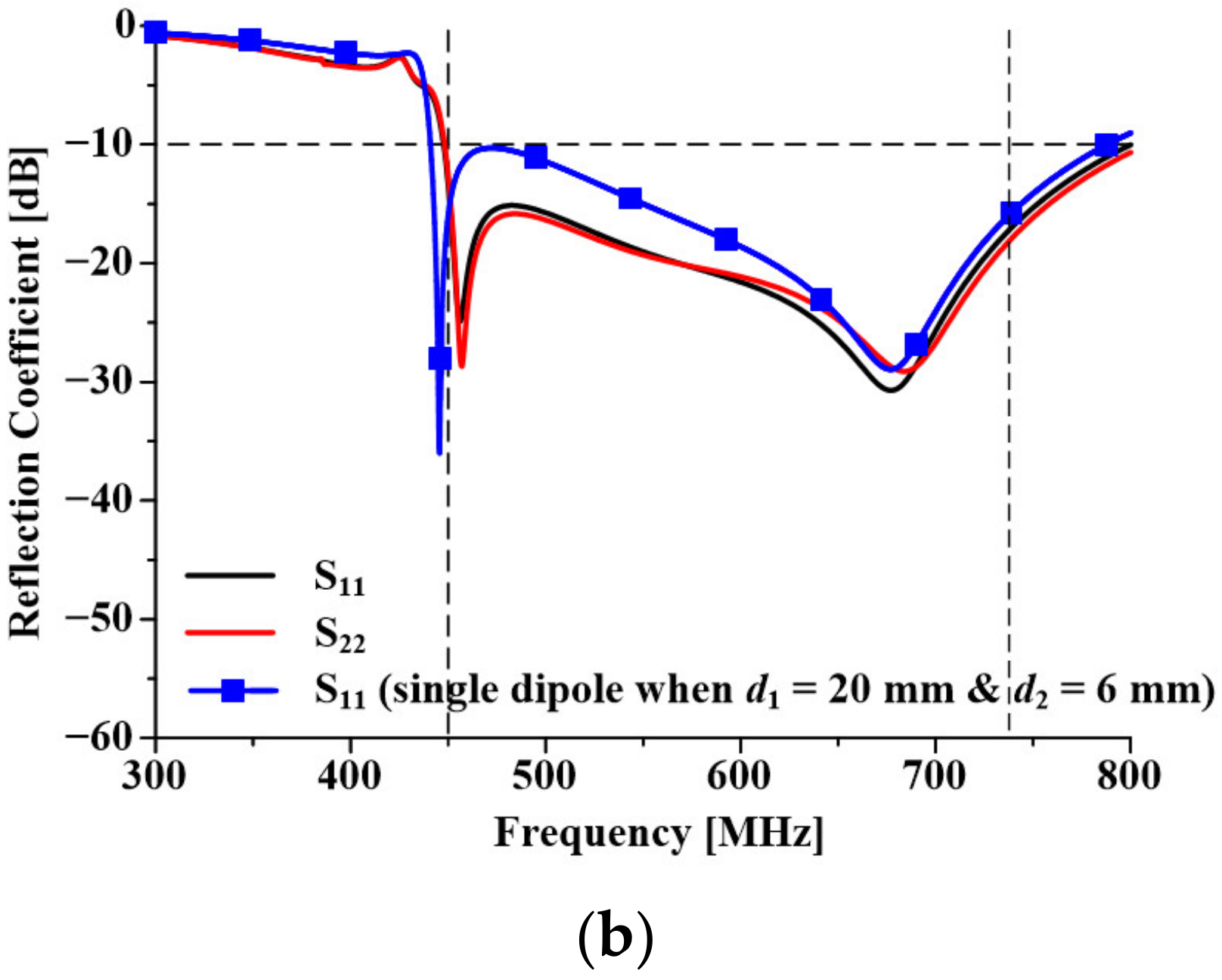
As shown in Figure 10a, two half bow-tie dipole antennas are assembled orthogonally to achieve dual-polarization characteristics. However, as shown in Figure 10b, the simulated −10 dB reflection coefficient performances are slightly shifted to a higher band in comparison with the performance of a single half bow-tie dipole antenna. In the case of a single half bow-tie dipole antenna (d1 = 20 mm and d2 = 6 mm), the simulated 10 dB |S11| band covers from 440.92 to 787.96 MHz. On the other hand, in the case of the antenna shown in Figure 10a, the simulated –10 dB reflection coefficient band covers from 447.7 to 800.91 MHz. It is considered that the operating band was changed due to the influence of antennas located nearby. Therefore, additional bandwidth enhancement in the lower band is required to cover the target band stably.
To shift the operating band to the lower band side slightly, we widened the width of the upper dipole arms, as shown in Figure 11a. However, the slope of the half bow-tie structure was unaltered (d2 = 6 mm). As a result, as shown in Figure 11b, the simulated –10 dB reflection coefficient band covers from 435.43 to 788.83 MHz; this is sufficient to cover the target band. Figure 11c shows the simulated radiation performance of the optimized dual-polarization half bow-tie dipole antenna. Because the radiation performances of the two antennas are identical, only the simulated result for the case of Port 1 excitation is shown. At 580 MHz, the simulated radiation gain is 2.51 dBi at θ = 0° and FBR is 2.06 dB.
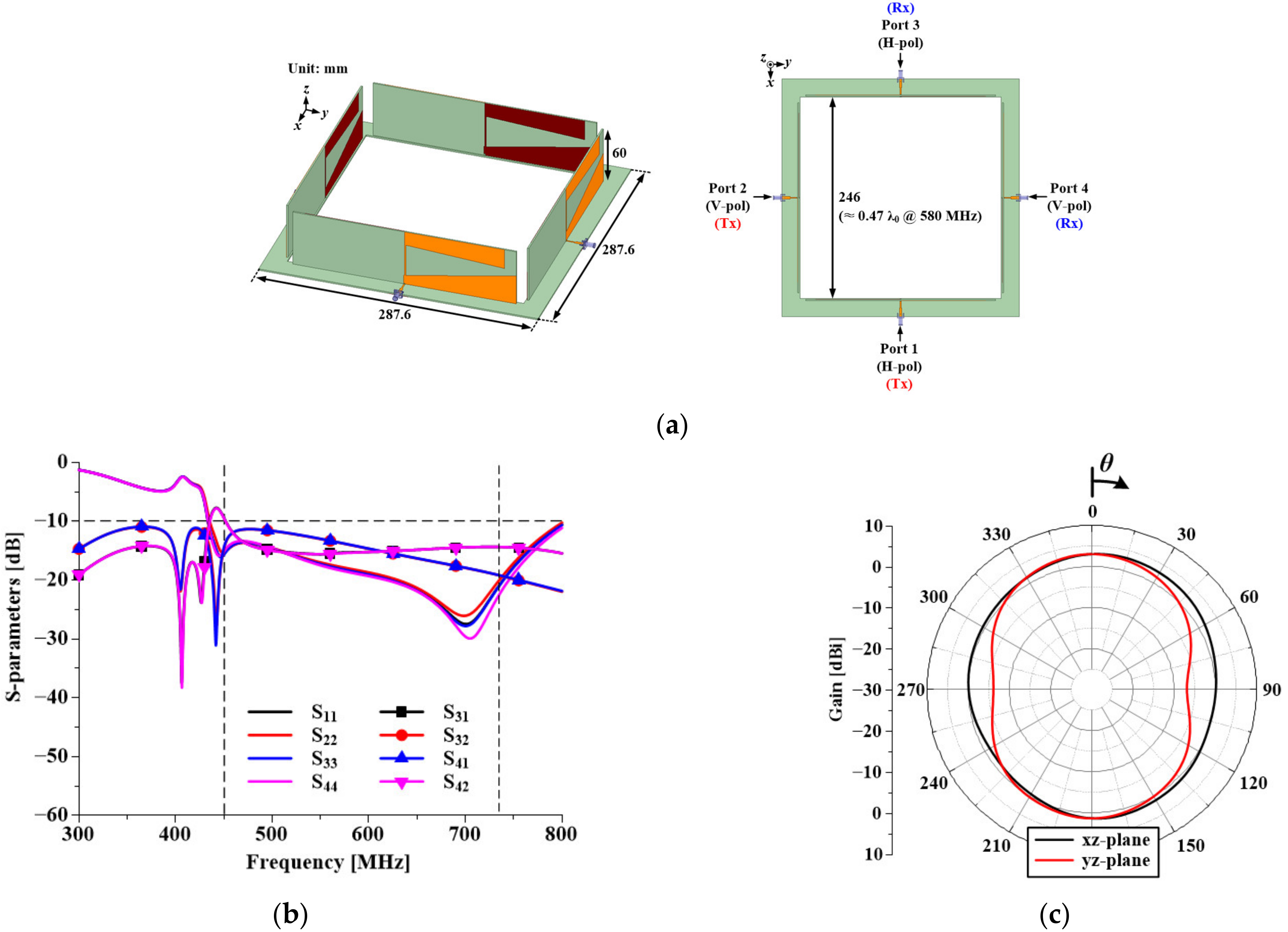
2.5. Dual-Polarization P-Band Tx/Rx Dipole Antenna Design and Performance
We assembled two optimized dual-polarization half bow-tie dipole antennas in an orthogonal manner to construct a Tx/Rx structure, as shown in Figure 12a. Ports 1 and 2 are included in the Tx part, and the other ports are included in the Rx part. Therefore, the designed Tx/Rx antenna can transmit and receive dual-polarized signals in the P-band. The simulated −10 dB reflection coefficient bands cover from 433.81 to 796.3 MHz. However, the simulated isolation (|SMN|) performances between the Tx and Rx ports are lower than 19.2 dB over the target band. Since all antennas are integrated in a limited space, the distance between the antennas is not sufficient to allow for high isolation characteristics. Figure 12c shows the simulated radiation performance at 580 MHz when Port 1 is excited. Since the designed Tx/Rx antenna has a symmetrical structure, the radiation characteristics of all antennas are identical. Therefore, only the simulated result for the case of Port 1 excitation is shown in this paper. At 580 MHz, the simulated radiation gain is 2.99 dBi at θ = 0° and FBR is 1.65 dB. The isolation characteristics can be improved by inserting an absorber, and this procedure will be discussed in the next section.
2.6. Fractal Absorber Design and Performance
As shown in Figure 13a, the basic unit cell of the metamaterial absorber with a fractal geometry was designed to enhance the low isolation characteristics in the P-band. A metallic fractal structure and a metal ground plane are printed on opposite sides of a 3.2 mm thick FR4 substrate. This fractal-shaped patch has a Minkowski fractal geometry, and this structure has been widely studied as a metamaterial absorber [12,13,14,15]. The advantage of this fractal-shaped absorber is that the resonance frequency can be easily tuned by only changing the fractal structure with a fixed substrate size [12,13]. An array of the fractal-shaped patches is equivalent to a series RLC circuit. Here, R takes into account dielectric/ohmic losses, L represents the inductance of the cell due to the magnetic flux between the patch and the metal ground plane, and C represents the parasitic capacitance between the edges of adjacent patches. For a fixed substrate, the best absorption performance can be achieved by proper optimization of the C values [13]. Figure 13b shows the simulation setup used to compute the S-parameters and absorptivity of the designed basic unit cell. Perfect electric conductor and perfect magnetic conductor boundary conditions are assigned in the xy- and xz-planes, respectively. The wave port is assigned in the yz-plane. The absorptivity can be calculated as A(ω) = 1 − |S21(ω)|2 − |S11(ω)|2, where |S11(ω)| and |S21(ω)| are magnitudes of the reflection and transmission coefficients, respectively [16]. However, the incident wave cannot propagate through the absorber due to the metal ground plane. Therefore, the magnitude of the transmission coefficient is zero, and the absorption can be expressed as A(ω) = 1 − |S11(ω)|2. Figure 13c shows the simulated S-parameters and the absorptivity of the designed basic unit cell. Nearly perfect absorption performance around 727.66 MHz is calculated (absorptivity of 98.34%); however, the resonance frequency needs to be moved to the lower frequency side around the center frequency of the target band.
The resonance frequency can be shifted to a lower band by changing the fractal-shaped patch. Figure 14a shows the structure of the optimized fractal geometry. The increased electrical length of the surface current leads to a lower resonance frequency without changing the substrate size. As shown in Figure 14b, the simulated absorption peak is formed around 602.65 MHz, with an absorptivity of 87.96%. To improve the isolation characteristics between the Tx and Rx antennas, the metamaterial absorber should be positioned diagonally in the proposed antenna structure. Therefore, we investigated the absorptivity performances depending on the incident angle, as shown in Figure 14c. When the wave is incident at an angle of 45°, a simulated absorptivity of 63.44% is achieved at 608.15 MHz.
Figure 15a shows a panel structure of the proposed metamaterial absorber. The panel consists of three layers, each of which is an 8 × 1 array of the optimized fractal-shaped patches. The proposed absorber consists of two back-to-back panels with a space of 3 mm between the panels. Figure 15b shows the structure in which the Tx/Rx antennas and the proposed absorber are combined. Figure 15c shows the simulated E-field distributions at 580 MHz for various absorber layers when Port 1 is excited. In the case without an absorber, the radiated wave propagates directly to the opposite antenna; this is the main reason for the low isolation characteristics. This propagation of the electromagnetic wave can be suppressed by inserting the proposed absorber. Metamaterial absorbers with different numbers of the fractal-shaped patch array layers are investigated in Figure 15c. As shown in Figure 15c, when the number of layers is less than three, suppression of the propagated wave is insufficient because the number of layers is not high enough to show the periodic characteristics [17]. Since it is difficult to increase the number of layers of the absorber to a very large number, an absorber with three layers is considered to be the optimized structure in this paper.
2.7. Proposed Antenna Design and Performance
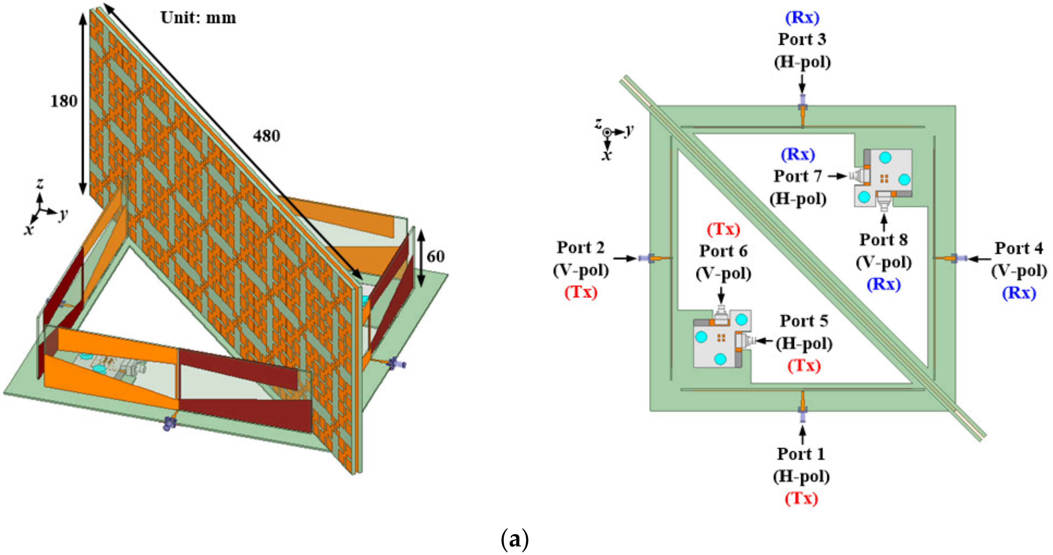
Figure 16a shows the proposed dual-band dual-polarization Tx/Rx antenna with the optimized metamaterial absorber. The 1.6 mm thick FR4 substrate containing the P-band feeding structures is shared with the reflectors of the Ka-band patch antenna array. Figure 16b shows the simulated S-parameters of the P-band dipole antennas. Since the proposed antenna structure is electrically large at 35 GHz, the simulation for the Ka-band antennas could not be carried out. The simulated −10 dB reflection coefficient band ranges from 311.26 to 838.12 MHz, which is sufficient to cover the targeted P-band. The simulated isolation characteristics are improved by inserting the metamaterial absorber. The simulated isolation characteristics are higher than 23.44 dB over the target band. Note that the simulated |S31| and |S42| improvements are approximately 28.94 dB and 40.56 dB at 609.23 MHz, respectively. As intended, remarkable improvement of the isolation characteristics is achieved around the resonance frequency of the absorber when it is tilted at 45°. To clearly show the effect of the metamaterial absorber on S-parameters, simulated S-parameter performances of the proposed antenna with and without metamaterial absorber are compared in Table 5. As shown in Table 5, both −10 dB reflection coefficient bandwidth and isolation characteristics in the target band are improved by inserting the absorber. Figure 16c shows the simulated radiation patterns at 580 MHz when Port 1 is excited. The simulated radiation gain is 1.83 dBi at θ = 0°, and FBR is 1.81 dB. The deterioration of the radiation performance is due to the influence of the metamaterial absorber.
3. Experimental Results
Figure 17 shows the fabricated antenna and its measured performances in the P-band. An antenna without the metamaterial absorber was also fabricated for comparison. The far-field radiation performance at 580 MHz was measured in an anechoic chamber. Figure 17d,f show the simulated and measured performances (reflection coefficient, isolation) of the proposed antenna with and without absorber. As shown in Figure 17d,f, the measured −10 dB reflection coefficient bands cover the target band, regardless of the presence of the absorber; however, the measured isolation characteristics are changed due to the absorber. Without the absorber, the measured isolation characteristics between the Tx and Rx antennas are lower than 20 dB over the target band. On the other hand, with the absorber, the measured isolation characteristics are higher than 20 dB over the target band. Figure 17b shows the simulated and measured radiation patterns at 580 MHz with the absorber. Measurements were performed when Port 1 was excited. The simulated and measured radiation gains at θ = 0° were 1.83 and 1.36 dBi, respectively. Discrepancies between the simulated and measured results may be caused by fabrication and measurement errors, such as slight misalignment between the reference antenna and the fabricated antenna.
Figure 18 shows the measured performances of the fabricated antenna in the Ka-band. As shown in Figure 18a, the measured −10 dB reflection coefficient bands fully cover the target band. Isolation characteristics between the Tx and Rx Ka-band antennas were measured, as shown in Figure 18b. Simulation could not be performed, because the proposed antenna structure is electrically large at 35 GHz. The distance between the Tx and Rx patch antenna arrays is 208 mm (≈24.26 λ0 at 35 GHz), which is sufficient to allow for high isolation characteristics. According to the measured results, isolation characteristics of more than 60 dB over the target band were achieved. Figure 18c shows the simulated and measured radiation patterns at 35 GHz when Port 5 is excited. The simulated and measured radiation gains were 10.25 and 8.49 dBi, respectively. The simulated FBR was 13.23 dB, although FBR measurements could not be performed due to the limitations of the rotating angle at the measurement facility.
4. Conclusions
In this paper, a dual-band dual-polarized antenna with improved isolation characteristics was proposed. A wide bandwidth in the P-band was achieved by using a half bow-tie dipole structure. Improvement of the isolation characteristics between the Tx and Rx antennas in the P-band was achieved by inserting a fractal-shaped metamaterial absorber. A 2 × 2 patch antenna array with aperture-coupled feeding was proposed to enhance the bandwidth in the Ka-band. Since the proposed antenna consists of qual-pol Tx/Rx antennas operating in the P- and Ka-bands, the proposed antenna can be a good candidate for PolSAR applications.
Author Contributions
The present work was carried out in collaboration between all the authors; D.P. and J.C. supervised the research. All authors have read and agreed to the published version of the manuscript.
Funding
This work was supported by a grant-in-aid of Hanwha Systems.
Institutional Review Board Statement
Not applicable.
Informed Consent Statement
Not applicable.
Data Availability Statement
Not applicable.
Conflicts of Interest
The authors declare no conflict of interest.
References
- Moreira, A.; Prats-Iraola, P.; Younis, M.; Krieger, G.; Hajnsek, I.; Papathanassiou, K.P. A Tutorial on Synthetic Aperture Radar. IEEE Geosci. Remote Sens. Mag. 2013, 1, 6–43. [Google Scholar] [CrossRef] [Green Version]
- Yang, J.; Yamaguchi, Y.; Lee, J.-S.; Touzi, R.; Boerner, W.-M. Applications of Polarimetric SAR. J. Sens. 2015, 2015, 316391. [Google Scholar] [CrossRef]
- Earthdata. Available online: https://earthdata.nasa.gov/learn/backgrounders/what-is-sar (accessed on 9 September 2021).
- Ouchi, K. Recent Trend and Advance of Synthetic Aperture Radar with Selected Topics. Remote Sens. 2013, 5, 716–807. [Google Scholar] [CrossRef] [Green Version]
- Zhou, S.-G.; Tan, P.-K.; Chio, T.-H. Wideband, low profile P- and Ku-band shared aperture antenna with high isolation and low cross-polarisation. IET Microw. Antennas Propag. 2013, 7, 223–229. [Google Scholar] [CrossRef]
- Kong, L.; Xu, X. A Compact Dual-Band Dual-Polarized Microstrip Antenna Array for MIMO-SAR Applications. IEEE Trans. Antennas Propag. 2018, 66, 2374–2381. [Google Scholar] [CrossRef]
- Balanis, C.A. Antenna Theory Analysis and Design, 3rd ed.; John Wiley & Sons Inc.: New York, NY, USA, 2005; pp. 813–815. [Google Scholar]
- Sulyman, A.I.; Nassar, A.T.; Samimi, M.K.; MacCartney, G.R., Jr.; Rappaport, T.S.; Alsanie, A. Radio propagation path loss models for 5G cellular networks in the 28 GHz and 38 GHz millimeter-wave bands. IEEE Commun. Mag. 2014, 52, 78–86. [Google Scholar] [CrossRef]
- Southwest Microwave. Available online: https://mpd.southwestmicrowave.com/product/1092-03a-6-end-launch-2-92mm-k-40-ghz-jack-female-standard-block/ (accessed on 9 September 2021).
- Lee, J.-I.; Yeo, J.; Han, D.-H. Design of planar dipole pair antenna for indoor digital TV reception. J. Korea Inst. Inf. Commun. Eng. 2014, 18, 2600–2606. [Google Scholar] [CrossRef] [Green Version]
- Lee, J.-I.; Yeo, J.; Park, J.-T. Compact half bow-tie-type quasi-Yagi antenna for terrestrial DTV reception. J. Korea Acad. Ind. Coop. Soc. 2013, 14, 1908–1914. [Google Scholar] [CrossRef] [Green Version]
- Dileep, A.; Abhilash, P.V.; Joy, V.; Singh, H.; Nair, R.U. Metamaterial absorber based on Minkowski fractal patch for stealth applications. In Proceedings of the 2020 IEEE International Conference on Electronics, Computing and Communication Technologies, Bangalore, India, 2–4 July 2020; pp. 1–4. [Google Scholar]
- Venneri, F.; Costanzo, S.; Massa, G.D. Fractal-shaped metamaterial absorbers for multireflections mitigation in the UHF band. IEEE Antennas Wirel. Propag. Lett. 2018, 17, 255–258. [Google Scholar] [CrossRef]
- Costanzo, S.; Venneri, F. Miniaturized fractal reflectarray element using fixed-size patch. IEEE Antennas Wirel. Propag. Lett. 2014, 13, 1437–1440. [Google Scholar] [CrossRef]
- Oloumi, D.; Ebadi, S.; Kordzadeh, A.; Semnani, A.; Mousavi, P.; Gong, X. Miniaturized reflectarray unit cell using fractal-shaped patch-slot configuration. IEEE Antennas Wirel. Propag. Lett. 2012, 11, 10–13. [Google Scholar] [CrossRef]
- Khuyen, B.X.; Tung, B.S.; Yoo, Y.J.; Kim, Y.J.; Lam, V.D.; Yang, J.G.; Lee, Y.P. Ultrathin metamaterial-based perfect absorbers for VHF and THz bands. Curr. Appl. Phys. 2016, 16, 1009–1014. [Google Scholar] [CrossRef]
- Kim, S.; Kim, D.K.; Kim, Y.; Choi, J.; Jung, K.-Y. A 24 GHz ISM-band Doppler radar antenna with high isolation characteristic for moving target sensing applications. IEEE Antennas Wirel. Propag. Lett. 2019, 18, 1532–1536. [Google Scholar] [CrossRef]
Figure 1.
Single patch antenna: (a) geometry of antenna, (b) perspective view, (c) side view, (d) simulated surface current distribution at 35 GHz, (e) simulated S-parameters, (f) simulated radiation patterns at 35 GHz when Port 1 is excited, and (g) simulated radiation patterns at 35 GHz when Port 2 is excited.


Figure 2.
2 × 2 patch antenna array for V-pol: (a) geometry of antenna array, (b) simulated surface current distribution at 35 GHz, (c) simulated reflection coefficient performances, and (d) simulated radiation patterns at 35 GHz.
Figure 2.
2 × 2 patch antenna array for V-pol: (a) geometry of antenna array, (b) simulated surface current distribution at 35 GHz, (c) simulated reflection coefficient performances, and (d) simulated radiation patterns at 35 GHz.

Figure 3.
2 × 2 patch antenna array for H-pol: (a) geometry of antenna array, (b) simulated surface current distribution at 35 GHz, (c) simulated reflection coefficient performances, and (d) simulated radiation patterns at 35 GHz.
Figure 3.
2 × 2 patch antenna array for H-pol: (a) geometry of antenna array, (b) simulated surface current distribution at 35 GHz, (c) simulated reflection coefficient performances, and (d) simulated radiation patterns at 35 GHz.


Figure 4.
2 × 2 patch antenna array with feeding network: (a) geometry of antenna array, (b) perspective view, (c) simulated S-parameters, (d) simulated radiation patterns at 35 GHz when Port 1 is excited, and (e) simulated radiation patterns at 35 GHz when Port 2 is excited.
Figure 4.
2 × 2 patch antenna array with feeding network: (a) geometry of antenna array, (b) perspective view, (c) simulated S-parameters, (d) simulated radiation patterns at 35 GHz when Port 1 is excited, and (e) simulated radiation patterns at 35 GHz when Port 2 is excited.


Figure 5.
2 × 2 patch antenna array with feeding network and reflector: (a) geometry of antenna array with reflector, (b) simulated S-parameters when h = 3 mm, (c) side view, (d) simulated radiation patterns at 35 GHz when Port 1 is excited (h = 3 mm), and (e) simulated radiation patterns at 35 GHz when Port 2 is excited (h = 3 mm).


Figure 6.
Assembled 2 × 2 patch antenna array: (a) geometry of antenna array, (b) perspective view, (c) simulated reflection coefficient performances, (d) simulated radiation patterns at 35 GHz when Port 1 is excited, and (e) simulated radiation patterns at 35 GHz when Port 2 is excited.
Figure 6.
Assembled 2 × 2 patch antenna array: (a) geometry of antenna array, (b) perspective view, (c) simulated reflection coefficient performances, (d) simulated radiation patterns at 35 GHz when Port 1 is excited, and (e) simulated radiation patterns at 35 GHz when Port 2 is excited.

Figure 7.
Single dipole antenna: (a) geometry of antenna, (b) simulated surface current density at 528 MHz, (c) simulated surface current density at 667 MHz, (d) simulated reflection coefficient performances for various g values, and (e) simulated radiation patterns at 580 MHz (g = 0.4 mm).
Figure 7.
Single dipole antenna: (a) geometry of antenna, (b) simulated surface current density at 528 MHz, (c) simulated surface current density at 667 MHz, (d) simulated reflection coefficient performances for various g values, and (e) simulated radiation patterns at 580 MHz (g = 0.4 mm).

Figure 8.
Orthogonal feeding structure of a single dipole antenna: (a) geometry of antenna, (b) simulated reflection coefficient performances depending on feeding structures, and (c) simulated radiation patterns at 580 MHz with orthogonal feeding structure.
Figure 8.
Orthogonal feeding structure of a single dipole antenna: (a) geometry of antenna, (b) simulated reflection coefficient performances depending on feeding structures, and (c) simulated radiation patterns at 580 MHz with orthogonal feeding structure.

Figure 9.
Half bow-tie dipole antenna: (a) geometry of antenna with various d1 values, (b) simulated reflection coefficient performances for various d1 values, (c) geometry of antenna with various d2 values (d1 = 20 mm), (d) simulated reflection coefficient performances for various d2 values (d1 = 20 mm), (e) simulated E-field distribution at 677 MHz when d1 = 20 mm and d2 = 6 mm, (f) simulated radiation performances versus frequency when d1 = 20 mm and d2 = 6 mm, (g) simulated radiation patterns at 450 MHz when d1 = 20 mm and d2 = 6 mm, (h) simulated radiation patterns at 580 MHz when d1 = 20 mm and d2 = 6 mm, and (i) simulated radiation patterns at 700 MHz when d1 = 20 mm and d2 = 6 mm.


Figure 10.
Dual-polarization half bow-tie dipole antenna: (a) geometry of antenna and (b) simulated reflection coefficient performances.
Figure 10.
Dual-polarization half bow-tie dipole antenna: (a) geometry of antenna and (b) simulated reflection coefficient performances.


Figure 11.
Optimized dual-polarization half bow-tie dipole antenna: (a) geometry of antenna, (b) simulated reflection coefficient performances, and (c) simulated radiation patterns at 580 MHz when Port 1 is excited.
Figure 11.
Optimized dual-polarization half bow-tie dipole antenna: (a) geometry of antenna, (b) simulated reflection coefficient performances, and (c) simulated radiation patterns at 580 MHz when Port 1 is excited.

Figure 12.
Dual-polarization Tx/Rx half bow-tie dipole antenna: (a) geometry of antenna, (b) simulated S-parameters, and (c) simulated radiation patterns at 580 MHz when Port 1 is excited.
Figure 12.
Dual-polarization Tx/Rx half bow-tie dipole antenna: (a) geometry of antenna, (b) simulated S-parameters, and (c) simulated radiation patterns at 580 MHz when Port 1 is excited.

Figure 13.
Basic unit cell of fractal absorber: (a) geometry of basic unit cell, (b) simulation setup, and (c) simulated S-parameters and absorptivity.
Figure 13.
Basic unit cell of fractal absorber: (a) geometry of basic unit cell, (b) simulation setup, and (c) simulated S-parameters and absorptivity.

Figure 14.
Optimized unit cell of fractal absorber: (a) geometry of optimized unit cell, (b) simulated S-parameters and absorptivity, and (c) simulated absorptivity performances depending on incident angle.
Figure 14.
Optimized unit cell of fractal absorber: (a) geometry of optimized unit cell, (b) simulated S-parameters and absorptivity, and (c) simulated absorptivity performances depending on incident angle.

Figure 15.
Proposed absorber: (a) geometry of an absorber panel, (b) dual-polarization Tx/Rx antenna with proposed absorber, and (c) simulated E-field distributions at 580 MHz for various absorber layers when Port 1 is excited.
Figure 15.
Proposed absorber: (a) geometry of an absorber panel, (b) dual-polarization Tx/Rx antenna with proposed absorber, and (c) simulated E-field distributions at 580 MHz for various absorber layers when Port 1 is excited.


Figure 16.
Proposed antenna: (a) geometry of proposed antenna, (b) simulated S-parameters of P-band, and (c) simulated radiation patterns at 580 MHz when Port 1 is excited.
Figure 16.
Proposed antenna: (a) geometry of proposed antenna, (b) simulated S-parameters of P-band, and (c) simulated radiation patterns at 580 MHz when Port 1 is excited.


Figure 17.
Fabricated antenna: (a) photographs of fabricated antenna, (b) simulated and measured radiation patterns at 580 MHz with absorber (when Port 1 is excited), (c) measurement setup of fabricated antenna without absorber, (d) simulated and measured performances (reflection coefficient, isolation) of the proposed antenna without absorber, (e) measurement setup of fabricated antenna with absorber, and (f) simulated and measured performances (reflection coefficient, isolation) of the proposed antenna with absorber.

Figure 18.
Measured results of Ka-band patch antenna array: (a) measured reflection coefficient performances of Ports 5 and 6, (b) measured isolation characteristics between Tx/Rx Ka-band patch antenna arrays, and (c) simulated and measured radiation patterns at 35 GHz when Port 5 is excited.
Figure 18.
Measured results of Ka-band patch antenna array: (a) measured reflection coefficient performances of Ports 5 and 6, (b) measured isolation characteristics between Tx/Rx Ka-band patch antenna arrays, and (c) simulated and measured radiation patterns at 35 GHz when Port 5 is excited.


Table 1.
Frequency bands used in SAR systems.
| Frequency Band | P | L | S | C | X | Ku | Ka |
|---|---|---|---|---|---|---|---|
| Frequency (GHz) | 0.3–1 | 1–2 | 2–4 | 4–8 | 8–12 | 12–18 | 27–40 |
Table 2.
Simulated radiation performances for various h values at 35 GHz.
| h (mm) (Wavelength at 35 GHz) | Polarization | Gain (dBi) (@ θ = 0°) | FBR (dB) |
|---|---|---|---|
| 1 (0.12 λ0) | V | 10.81 | 20.66 |
| H | 10.23 | 22.24 | |
| 2 (0.23 λ0) | V | 10.89 | 23.6 |
| H | 10.69 | 22.25 | |
| 3 (0.35 λ0) | V | 10.89 | 27.36 |
| H | 10.78 | 22.76 | |
| 4 (0.47 λ0) | V | 10.88 | 15.12 |
| H | 10.77 | 18.1 | |
| 5 (0.58 λ0) | V | 12.39 | 8.82 |
| H | 11 | 10.64 |
Table 3.
Simulated −10 dB reflection coefficient performances for various h values.
| h (mm) (Wavelength at 35 GHz) | Polarization | −10 dB Reflection Coefficient Band (GHz) |
|---|---|---|
| 1 (0.12 λ0) | V | 31.66–36.17 |
| H | 29.05–37.61 | |
| 2 (0.23 λ0) | V | 32.58–38.10 |
| H | 29.33–36.99 | |
| 3 (0.35 λ0) | V | 32.90–37.72 |
| H | 32.21–36.89 | |
| 4 (0.47 λ0) | V | 33.04–35.62 |
| H | 32.27–39.63 | |
| 5 (0.58 λ0) | V | 33.50–36.10 |
| H | 27.78–37.24 |
Table 4.
Simulated radiation performances when d1 = 20 mm and d2 = 6 mm.
| Frequency (MHz) | Gain (dBi) (@ θ = 0°) | FBR (dB) |
|---|---|---|
| 450 | 4.49 | 7.42 |
| 580 | 2.62 | 2.37 |
| 700 | 4.23 | 3.04 |
Table 5.
Simulated S-parameter performances of the proposed antenna with and without metamaterial absorber.
Table 5.
Simulated S-parameter performances of the proposed antenna with and without metamaterial absorber.
| Structure | −10 dB Reflection Coefficient Band | Isolation (|SMN|) in Target Band |
| Without metamaterial absorber | 433.81–796.3 MHz | |SMN| < 19.2 dB |
| With metamaterial absorber | 311.26–838.12 MHz | |SMN| > 23.44 dB |
Publisher’s Note: MDPI stays neutral with regard to jurisdictional claims in published maps and institutional affiliations. |
© 2021 by the authors. Licensee MDPI, Basel, Switzerland. This article is an open access article distributed under the terms and conditions of the Creative Commons Attribution (CC BY) license (https://creativecommons.org/licenses/by/4.0/).
Share and Cite
MDPI and ACS Style
Park, D.; Choi, J. A Dual-Band Dual-Polarized Antenna with Improved Isolation Characteristics for Polarimetric SAR Applications. Appl. Sci. 2021, 11, 10025. https://0-doi-org.brum.beds.ac.uk/10.3390/app112110025
AMA Style
Park D, Choi J. A Dual-Band Dual-Polarized Antenna with Improved Isolation Characteristics for Polarimetric SAR Applications. Applied Sciences. 2021; 11(21):10025. https://0-doi-org.brum.beds.ac.uk/10.3390/app112110025
Chicago/Turabian StylePark, Daesung, and Jaehoon Choi. 2021. "A Dual-Band Dual-Polarized Antenna with Improved Isolation Characteristics for Polarimetric SAR Applications" Applied Sciences 11, no. 21: 10025. https://0-doi-org.brum.beds.ac.uk/10.3390/app112110025
Note that from the first issue of 2016, this journal uses article numbers instead of page numbers. See further details here.