Article

Application of Single-Phase Supply AC-DC-AC VFD for Power Factor Improvement in LED Lighting Devices Loaded Power Distribution Lines

by
Gytis Petrauskas
1,* and
Gytis Svinkunas
2
1
Department of Automation, Faculty of Electrical and Electronics Engineering, Kaunas University of Technology, LT-51394 Kaunas, Lithuania
2
Department of Electric Power Systems, Faculty of Electrical and Electronics Engineering, Kaunas University of Technology, LT-51394 Kaunas, Lithuania
*
Author to whom correspondence should be addressed.
Submission received: 23 May 2022 / Revised: 6 June 2022 / Accepted: 8 June 2022 / Published: 11 June 2022
(This article belongs to the Collection Advanced Power Electronics in Power Networks)

Abstract

:
More and more light-emitting diode lighting devices (LED) are being connected to modern power distribution lines. In addition to its many positive features, this poses problems in terms of reactive power compensation. The large number of LEDs interacting with traditional reactive power compensators leads to a harmful phenomenon—overcompensation. This was experimentally determined in the investigated power distribution lines. Along with LEDs, a large number of devices with variable frequency drives (VFD) are connected to the same power distribution lines. This study presents an innovative approach to conventional diode rectifier supply side AC-DC-AC VFDs. It is proposed to use these VFDs as a reactive power compensation device while maintaining their main functions—motor powering and motor speed control. Minor improvements have been proposed to enable these VFDs to provide and draw out reactive power, thereby keeping power factors close to the unit in LED-loaded power distribution lines. The proposed improvements are based on the interaction between the power distribution lines inductivity and the DC circuit capacitance of the VFD. It has been shown that the power factor can be controlled by varying the capacity of the DC circuit. The ability of the AC-DC-AC VFD to compensate for the reactive power provided by the light-emitting diode lighting devices was confirmed by mathematical calculations and experimentally with a laboratory prototype.

Graphical Abstract

1. Introduction

Nowadays, the LED lighting devices are increasingly becoming our main source of artificial light in many applications. This is due to reductions in manufacturing cost and their excellent characteristics in comparison to conventional lighting solutions. The main applications are street lighting, residential lighting, automotive, and LED wall displays for advertising placement. The main economic advantages of LEDs are low maintenance requirements, long lifetime and reliability and high-power density. The main technical advantages are controllability in both light and color, lack of warm-up period, and luminous efficiency. In addition, LEDs are an environment-friendly source of artificial light [1].
Despite the above advantages, most LED light sources are powered by a two-stage electronic driver without power factor correction equipment [
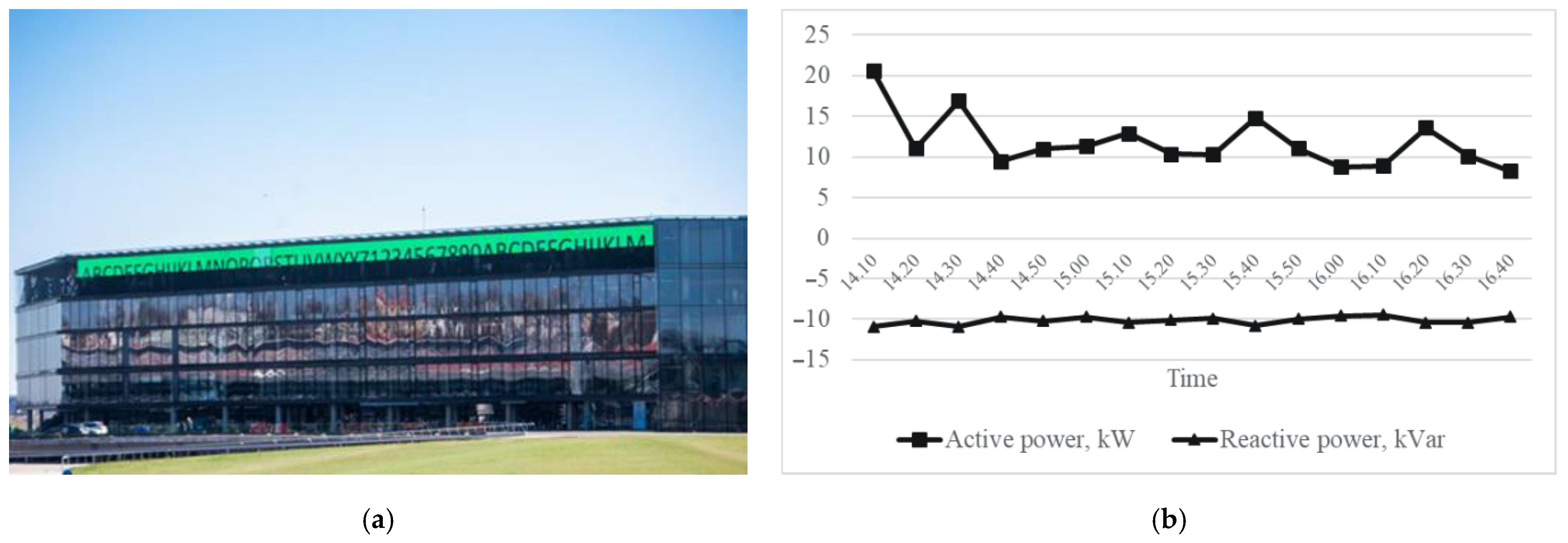
2]. An example is the 32 kW LED wall display presented in Figure 1a. It is a source of the leading reactive power. By the interaction of LED with a conventional capacitors-based reactive power compensation device, the reactive power of the leading character is further increased. 
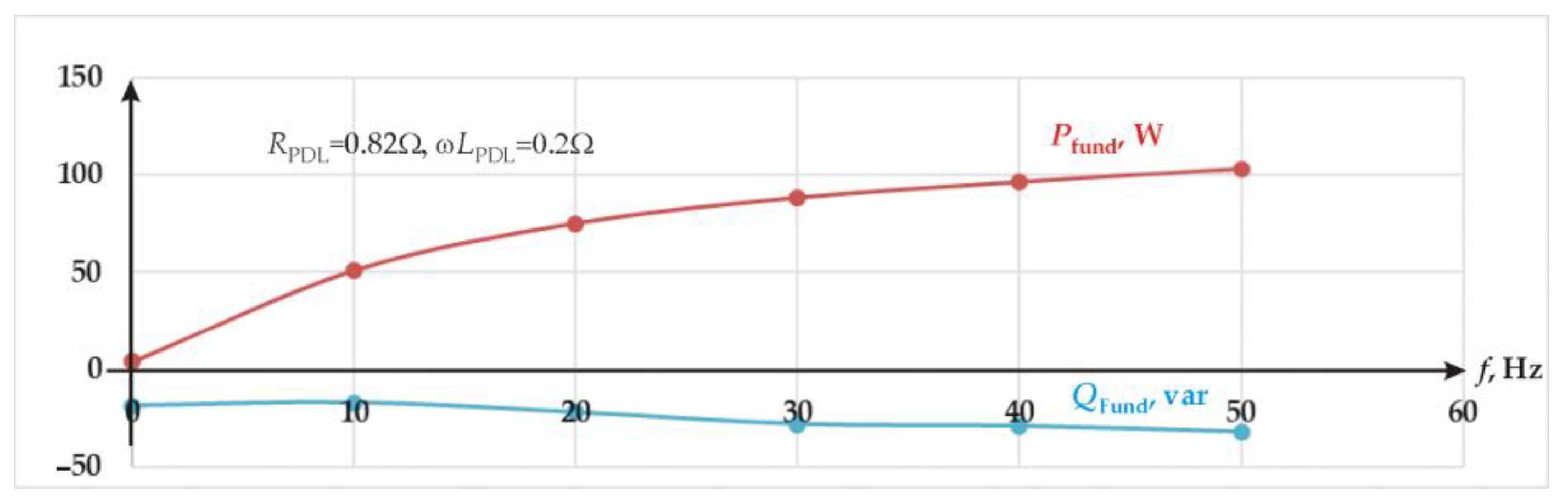
Figure 1b shows the values of the active and reactive power caused by the 32 kW LED wall display. These data are experimentally collected at a sports arena, where the DA80.1600RGB-50M LED wall display is installed.
These data were collected during bright daytime, as the brightness of the screen was at that time the highest. These data show that regardless of the active power consumption, this LED wall display provided reactive power in the range of 9.5 ÷ 10.9 kVar. The conventional capacitors-based built-in reactive power compensation device in this arena has not compensated this reactive power. As a result, the company that operates this sports arena pays huge fines to the electric power supply company.
For the electronic equipment connected to the power distribution line (PDL), the power factor shows an efficiency measure for the usage of electrical energy. The power factor improvement reduces the load on the power grid transformers and PDL conductors, leading to a reduction in the energy losses [3].
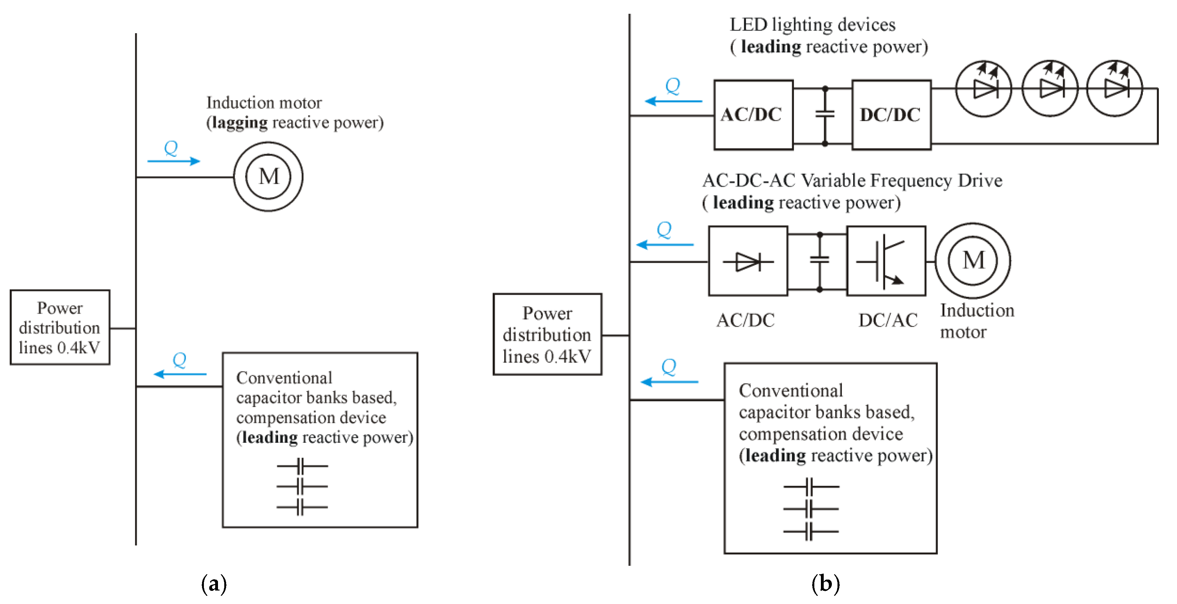
Local reactive power compensation devices are used as a standard to improve the power factor. Typically, the current in conventional PDL lags behind voltage because of inductive loads such as AC motors [
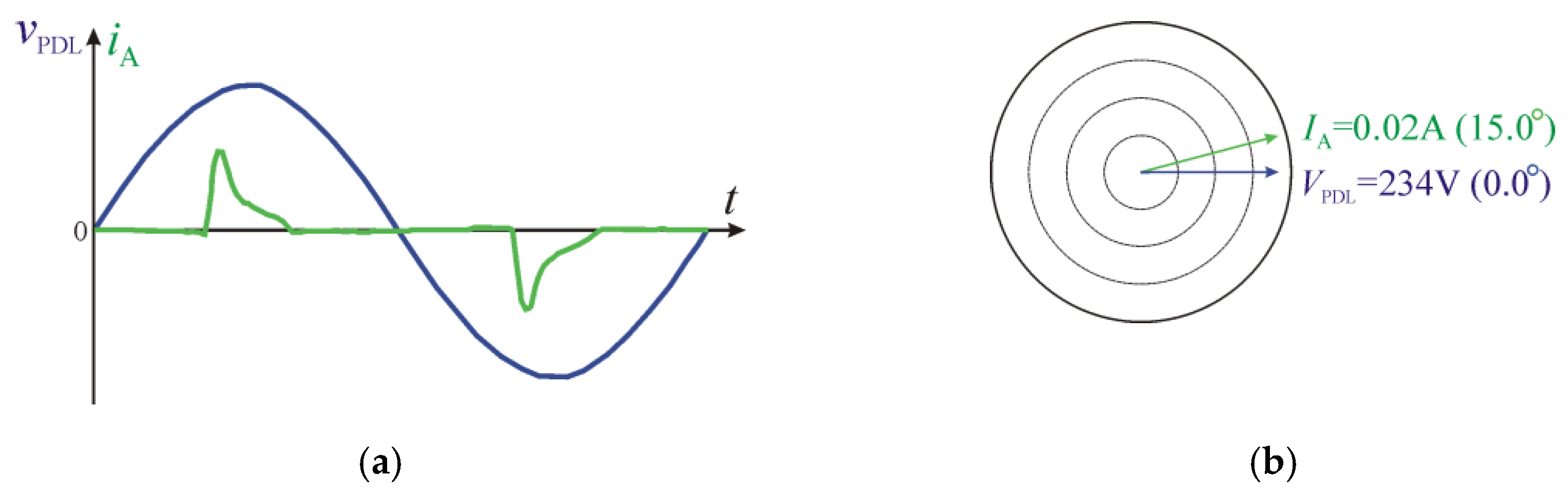
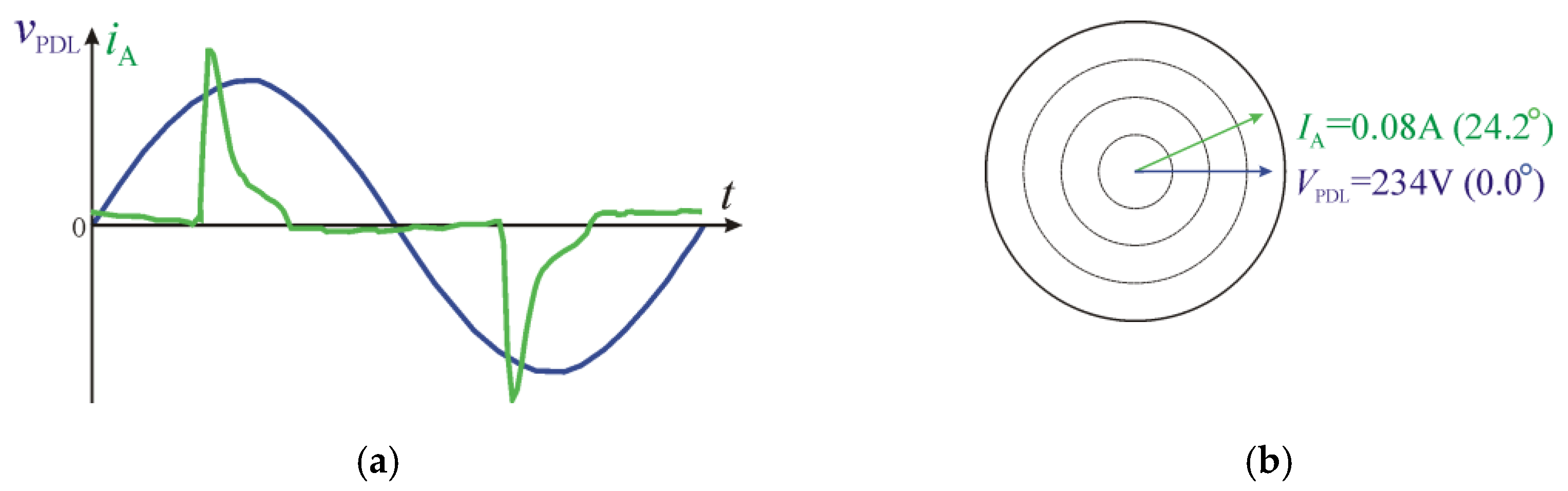
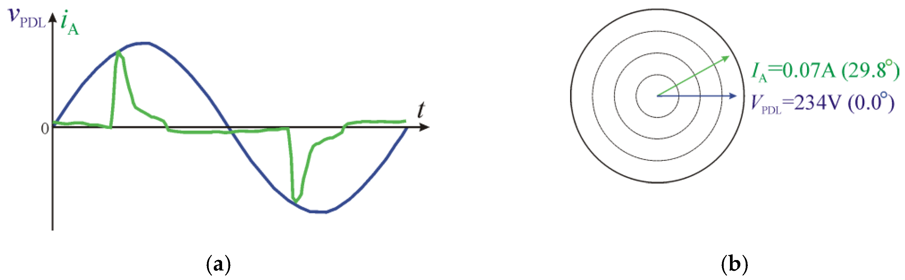
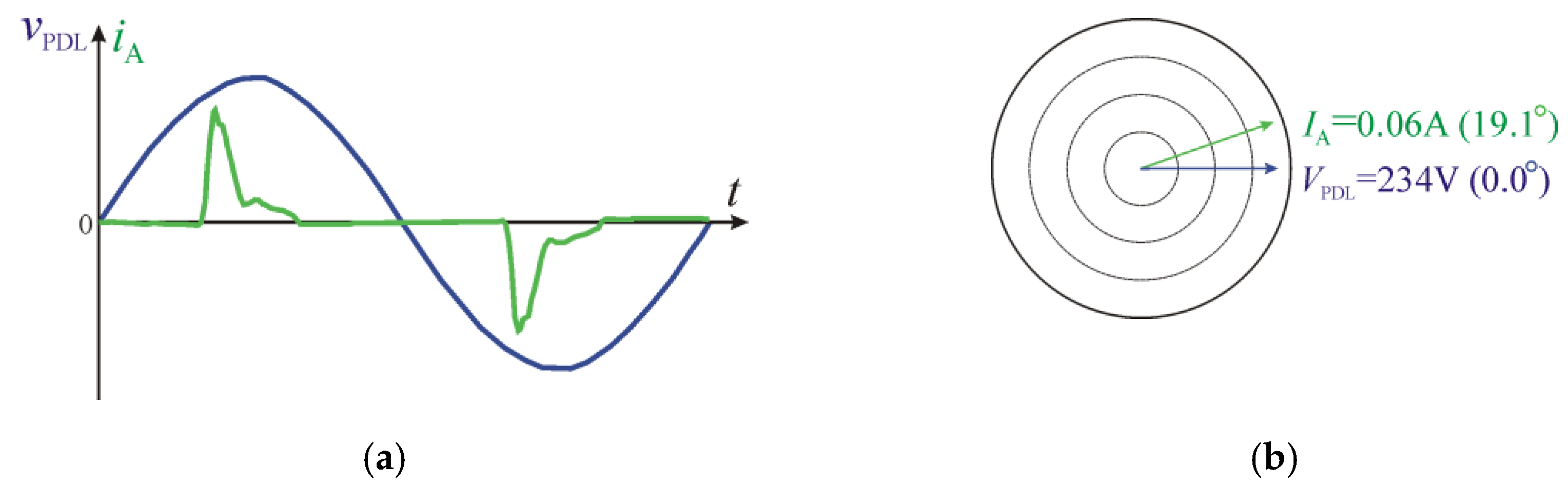
4]. Local, capacitance-based reactive power compensation devices are usually designed to compensate the lagging reactive power. The application of energy-efficient light-emitting diode LED lighting sources reduces the power demand by about 30% relative to the currently available sources. Unfortunately, these systems are, in many cases, the source of disturbances that further reduce the power factor. The evolution of LED light technology and VFD technology has changed the type of reactive power available in 0.4 kV PDL (Figure 2).
Various methods of reactive power compensation have been proposed in scientific publications. The publication [4] proposed the use of a matrix converter-based variable frequency drive (VFD) to compensate the reactive power provided by LED lighting devices. However, matrix VFDs are innovative VFDs and are not yet widely used. The authors of the study [5] suggest the use of an alternating current/direct current converter for prosumer applications. However, the implementation of this compensation method requires costly additional equipment. The authors of the study [6] suggest the use of a three-phase star-connected Buck-type dynamic capacitor. However, this measure is suitable for compensating the lagging type reactive power. The publication [7] examines in detail and summarizes the power quality coefficients that can be applied to AC-DC-AC VFD-loaded PDL. The power factor is applied as the universal criterion for the electromagnetic compatibility of distorted current in PDL and distorting loads. However, ways to reduce the distortion and reactive power are not presented. The publication [8] presents an LED driver consisting of an interleaved buck-boost power factor correction (PFC) converter with coupled inductors and a half-bridge LLC resonant converter. Using this driver reduces the reactive power provided in the PDL. However, the integrated buck-boost PFC converter with coupled inductors significantly increases the cost of this driver. The publication [9] presents a two-stage LED driver based on commercial integrated circuits. The first stage consists of an AC-DC power factor correction unit. The second stage consists of a DC/DC power converter. This two-stage LED driver, as with the driver presented in [9], improves the power factor but increases the cost of LED light devices due to its complexity. The publication [10] presents a high-power factor LED driver. Using such a driver in LED light devices would not cause the aforementioned problems with power factor correction. In addition, there would be no need for the proposed method of compensation. However, this is the technology of the future and will not solve the above-mentioned power factor problems caused by already installed LED light devices. A publication [11] presents a power factor improvement method based on teaching–learning-based optimization. Using this method, the optimal capacitor combination to improve the power factor is calculated. However, this method is only applicable in the presence of lagging reactive power and is not suitable for compensating the reactive power of LED light devices. Various methods for reactive power compensation have been presented in [12]. One of them, using Thyristorized Var Compensators, can compensate for both types of leading and lagging reactive power. This approach would be appropriate to address the problems mentioned above. However, the use of Thyristorized Var Compensators involves additional investment and financial costs. The Static var Compensator presented in [13] also requires additional investment and financial costs.
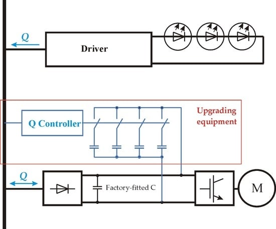
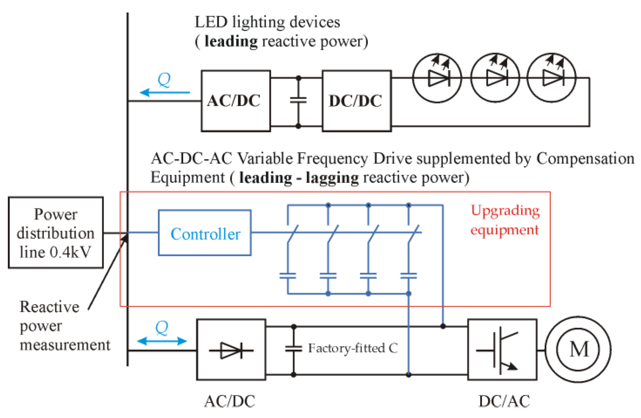
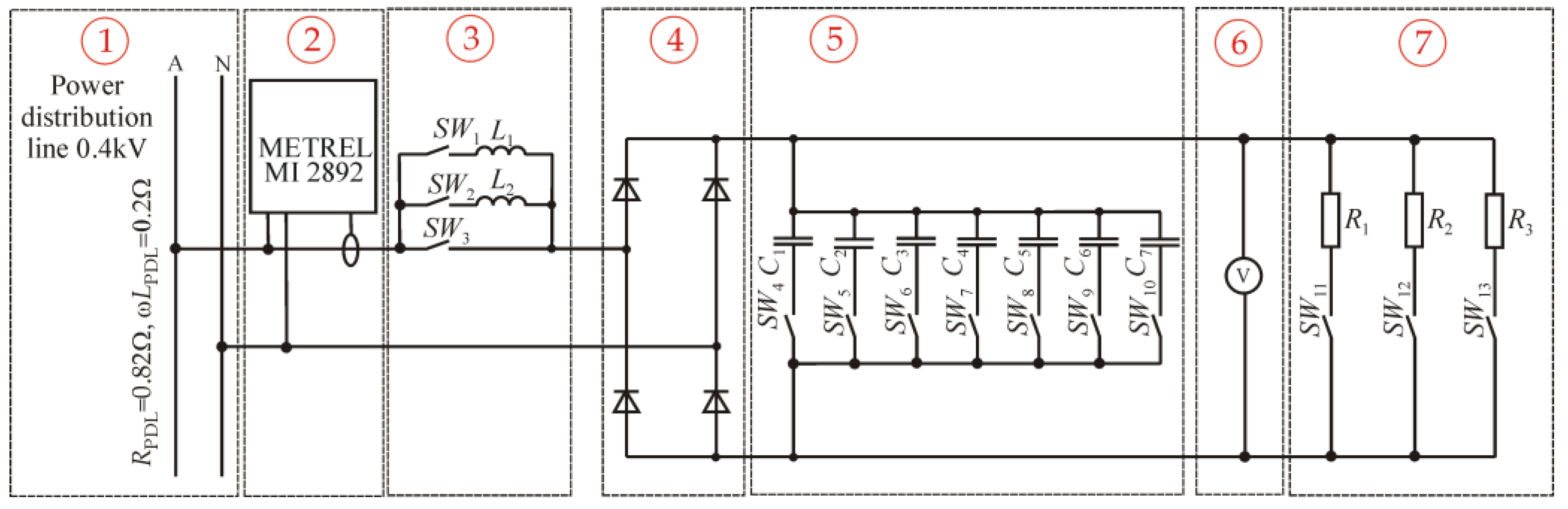
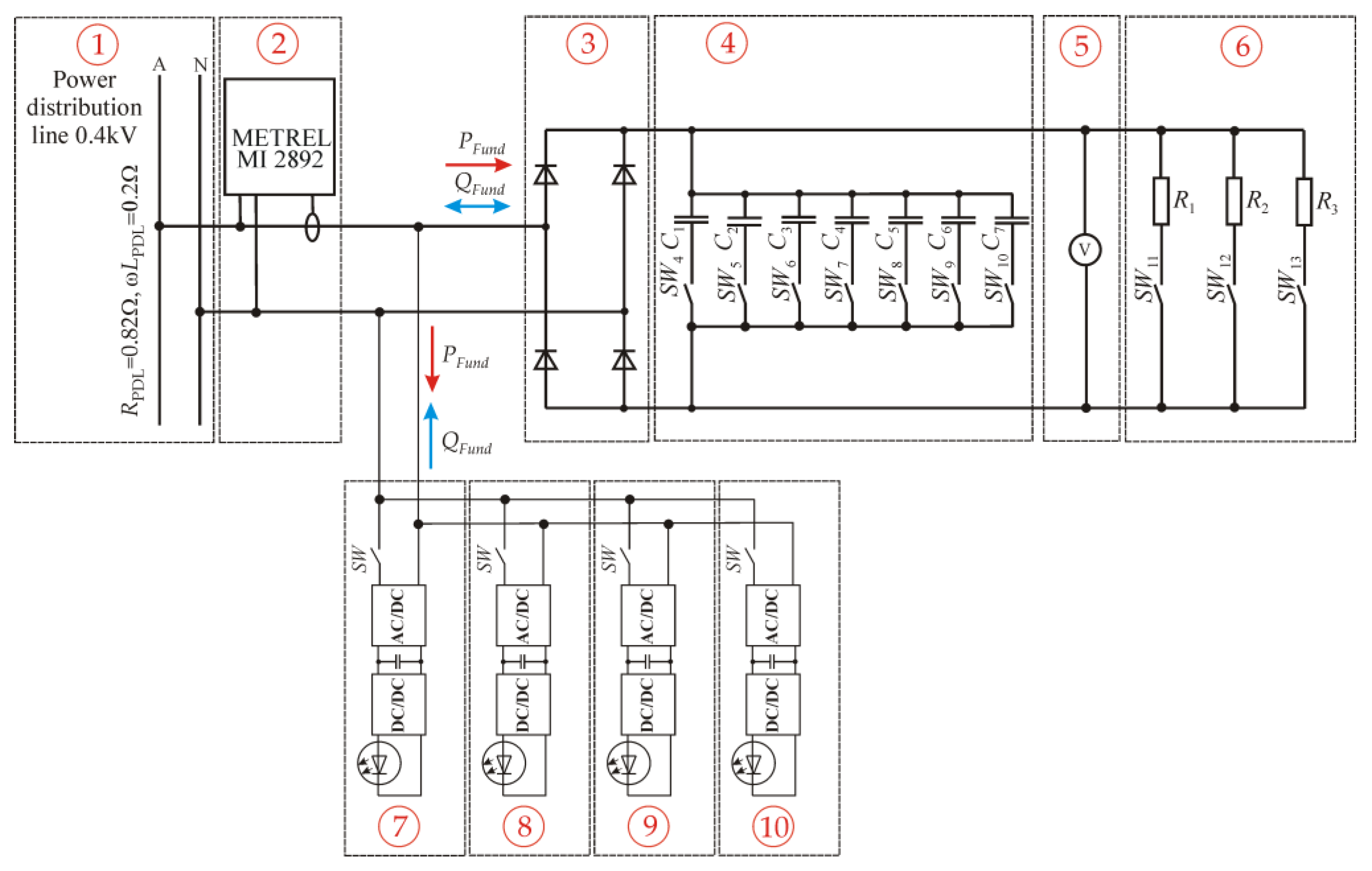
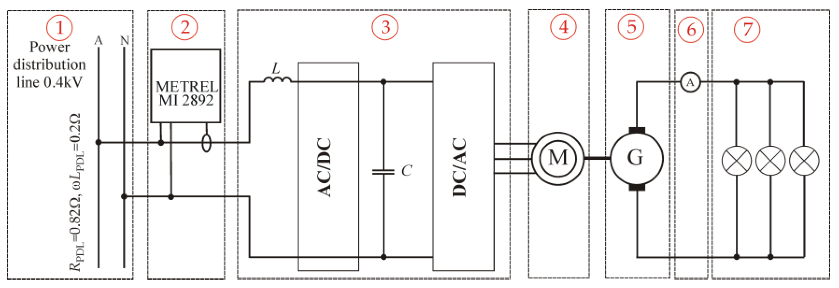
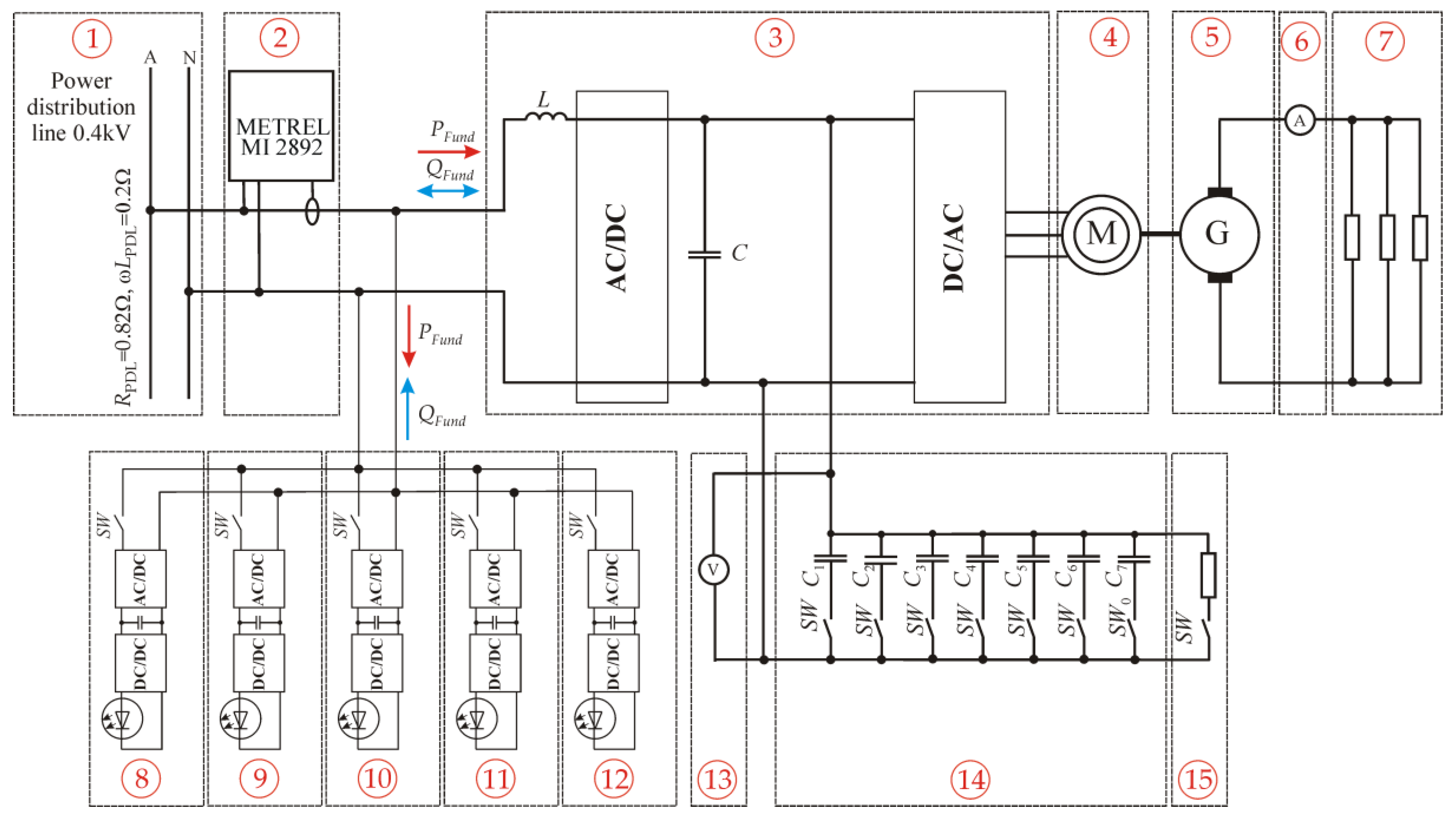
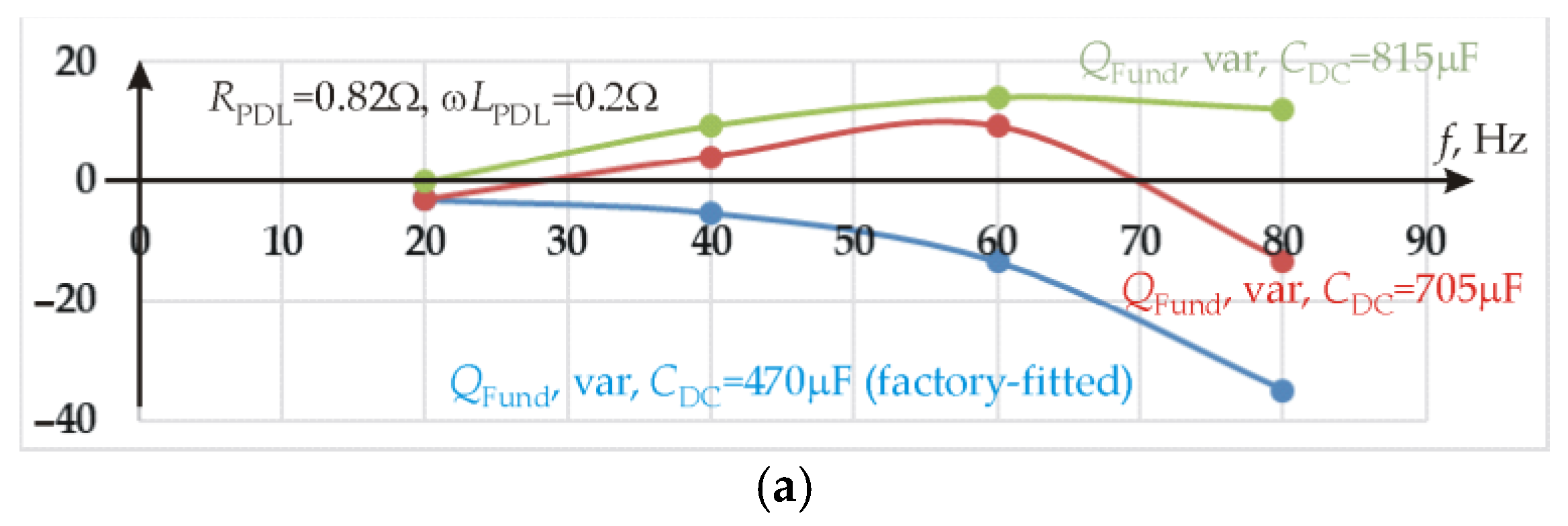
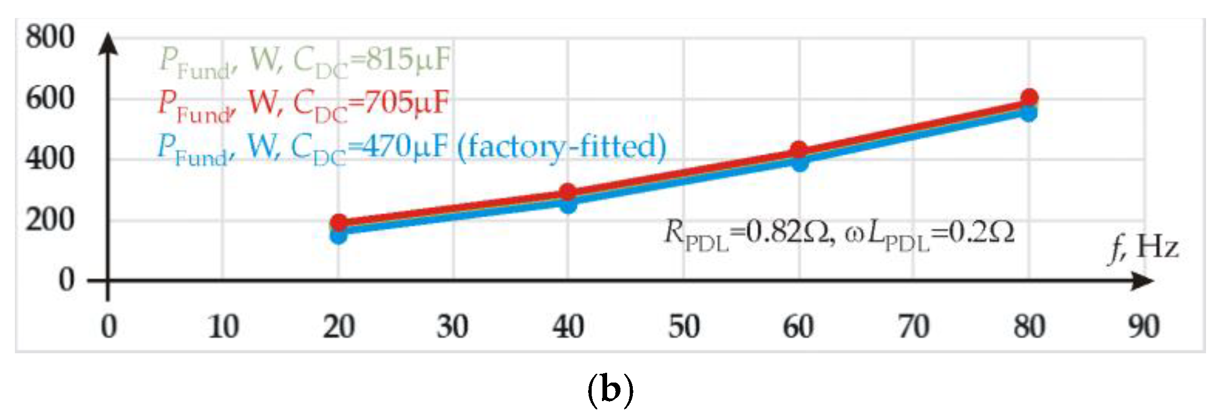
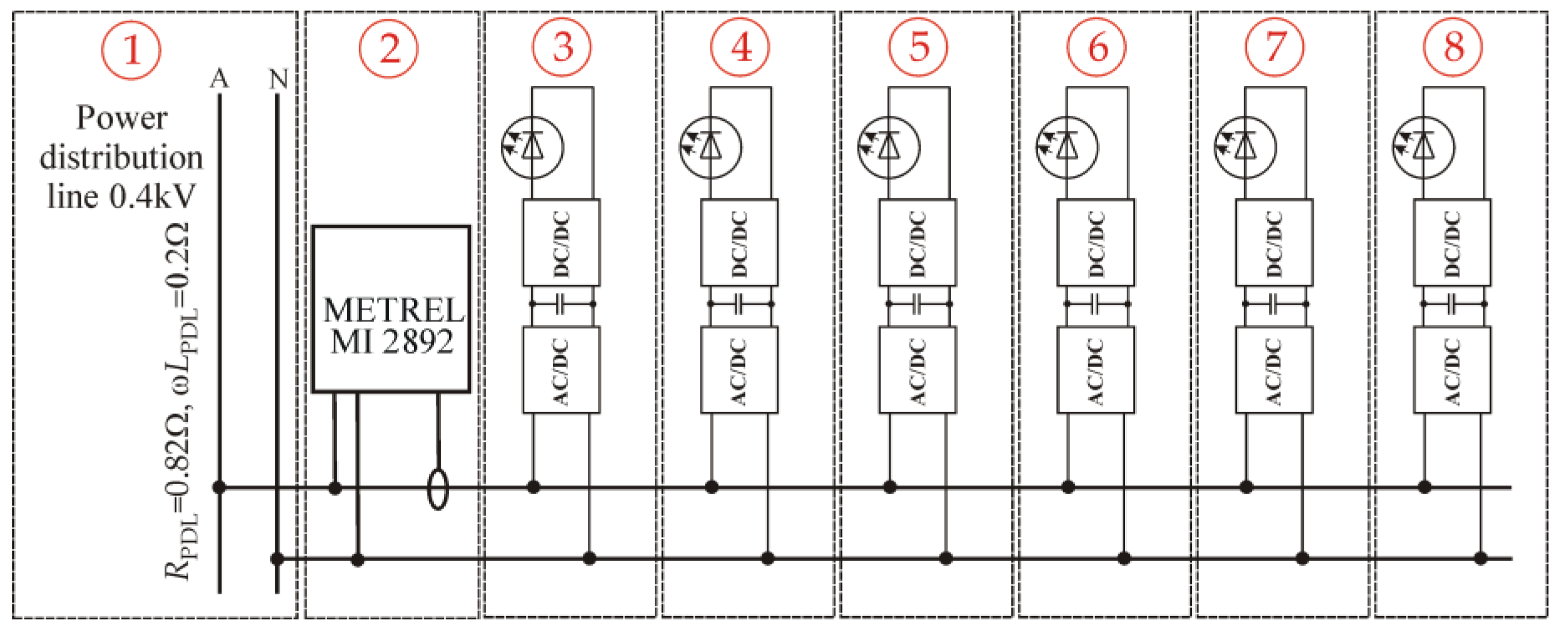
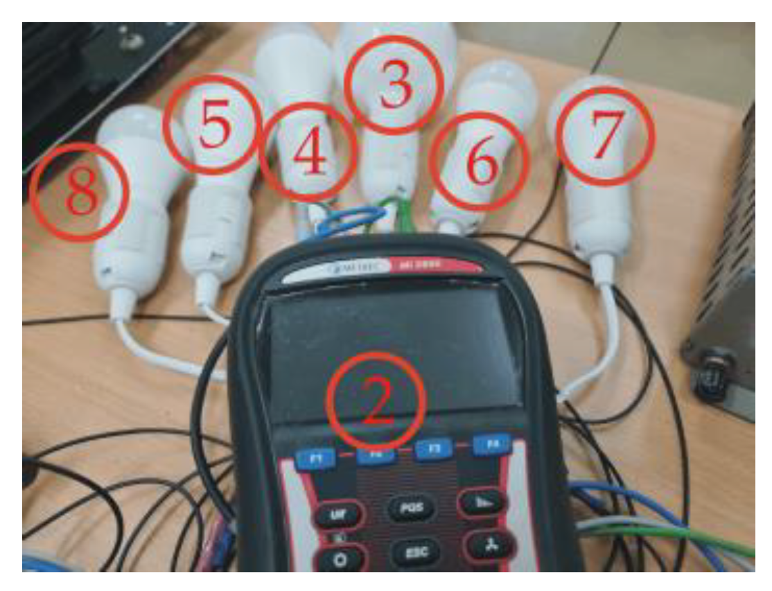
The global VFD market size was valued at USD 22.5 billion in 2021 and is expected to grow at a compound annual growth rate of 6.5%. Most industrial and entertainment buildings equipped with LEDs are also equipped with a large amount of AC-DC-AC VFDs. These VFDs are used to power the induction motor of fans, pumps and other equipment. About 70 AC-DC-AC VFDs have been installed in the aforementioned sports arena. A further study examined the reactive power provided by LEDs and single-phase supply conventional AC-DC-AC VFD. The possibility of modernizing the VFD by supplementing the DC circuit with capacitors, at the same time transforming the VFD into a reactive power compensation and power factor improvement device, was investigated (Figure 3). This possibility of modernization has been tested mathematically and experimentally.
Applying the VFD improvement proposed in this article could improve the PDL power factor with relatively little investment. This is an advantage in terms of energy costs and, at the same time, in terms of ecology and climate change. The low cost of the compensation method is due to the fact that no additional expensive compensation equipment based on inductive reactors is required. It is enough to modernize the already installed VFD by adding low-cost components—electrolytic capacitors, small control and switching means. This is an advantage over the method presented in [2], which proposes to replace a conventional AC-DC-AC converter with a direct AC-AC converter in a number of already installed VFDs.
The remainder of the paper will be organized as follows. Section 2 of the paper provides a mathematical analysis of the reactive power in PDL loaded by a supply-side rectifier VFD. It is shown mathematically that the capacitance of a DC circuit capacitor affects the nature and value of the reactive power. Section 3 provides an experimental analysis of reactive power. The nature and value of the reactive power of each of the major devices connected to modern PDLs were analyzed separately. Experimental analysis of the reactive power in PDL loaded by LED lighting devices is provided in Section 3.1. Experimental analysis of the reactive power in the PDL loaded by diode rectifier supply-side devices is provided in Section 3.2. Experimental analysis of the reactive power in the PDL loaded by LED light and diode rectifier supply-side devices is provided in Section 3.3. An experimental analysis of the reactive power in the PDL loaded by the diode rectifier supply-side variable frequency drive is provided in Section 3.4. Section 4 presents an experimental analysis of reactive power in VFDs and LEDs-loaded PDLs. The ability of the VFD to compensate for the reactive power produced by the LED and to achieve a power factor close to that unit has been experimentally confirmed. Section 5 discusses the results of this study.

2. Theoretical Background for Interaction between the Power Distribution Lines Inductivity and the DC Circuit Capacitance of the VFD

2.1. Operating Modes of the VFD’s Supply Side Rectifier
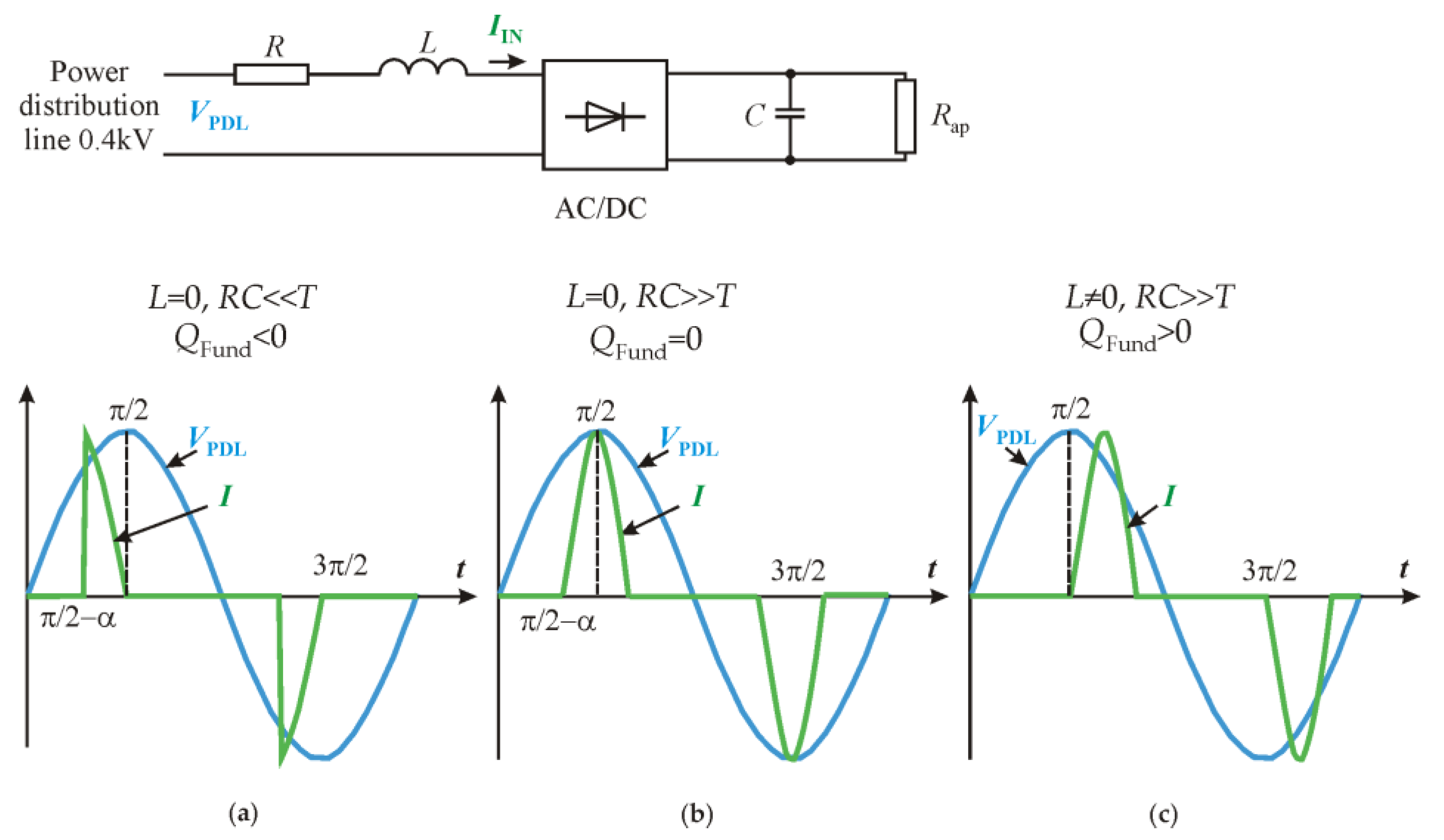
Publication [4] demonstrates that a VFD rectifier connected between a PDL and a DC circuit capacitor of the VFD provides the leading reactive power (QFund < 0). The reason for this is the displacement of the pulse of the input current drawn by the VFD rectifier with respect to the voltage of PDL. The input current pulse reaches its maximum value in time before the sinusoidal voltage of the PDL reaches its maximum point (the current leads against the voltage 
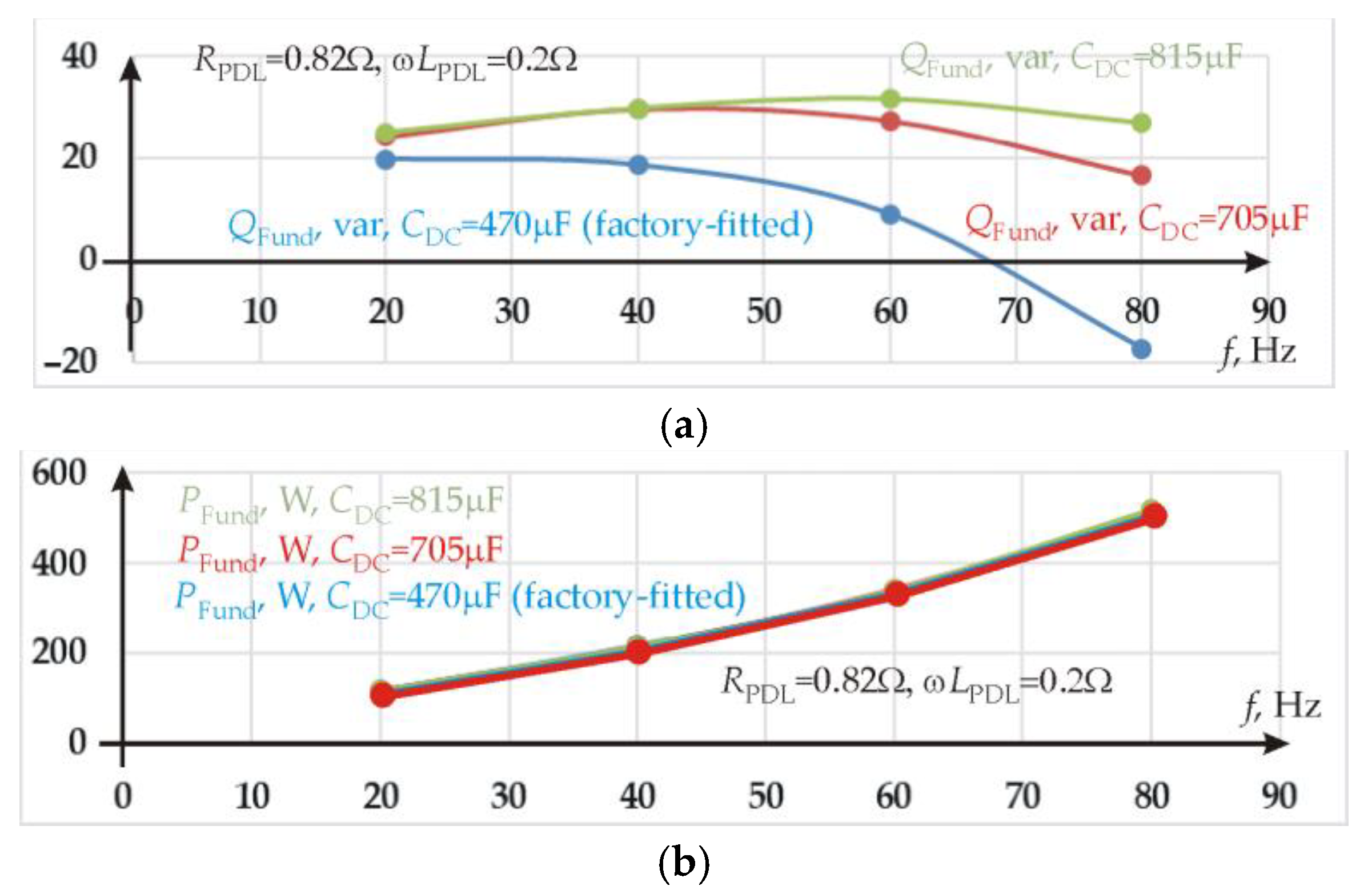
Figure 4a). These processes require a relatively small capacity DC circuit capacitor and a low PDL resistance; otherwise, the DC capacitor will not be able to charge until the voltage reaches a maximum. Subsequent experimental studies used a 1 kW rated power VFD with an original 470 µF DC circuit capacitor installed.
A different process uses a capacitor with a capacitance greater than the minimum required capacity in the VFD DC circuit and a higher PDL resistance. In this case, conditions will be reached where the maximum values of the pulse of the input current drawn by the VFD rectifier and the PDL voltage coincide in time. In this case, the reactive power provided or drawn out by the VFD will be zero (QFund = 0) (Figure 4b).
Experimental studies have shown that conventional VFD can be a source of lagging reactive power (QFund > 0). This is due to the high capacity of the VFD DC circuit and the PDL inductivity. In this case, in the process of interaction between the DC link capacity of the VFD and the inductivity of the PDL, the maximum value of the pulse of the input current drawn by the VFD rectifier lags behind the maximum value of the sinusoidal voltage of the PDL (Figure 4c).

2.2. The Initial Operation Conditions of the VFD’s Supply-Side Rectifier

As highlighted in the publication [2], to compensate the reactive power provided by the LED, the conventional VFD must operate in the mode shown in Figure 4c. Under the conventional VFD mode shown in 
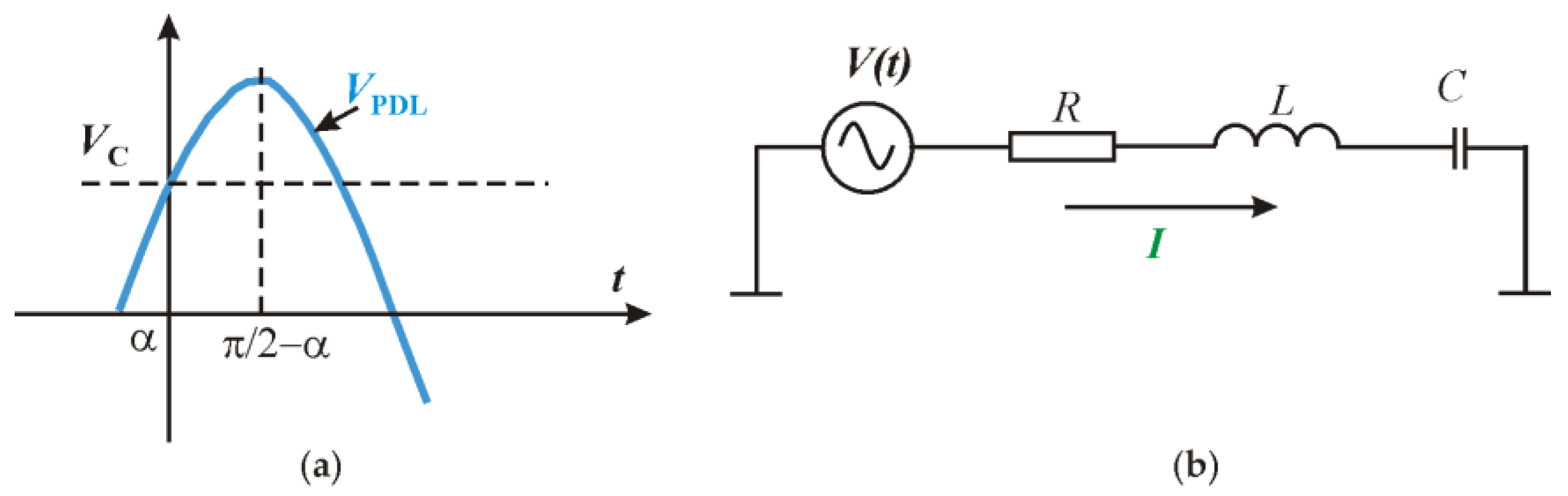
Figure 4b, the effect on PDL reactive power will be neutral. In describing this mathematically, the aim is to describe the capacitor voltage VC at steady state and the angle of displacement α of the input current pulse.
The current flows through the diodes of the VFD rectifier at the time interval when the voltage of the PDL v(t) is higher than the voltage of the capacitor of the VFD DC circuit vc. Assuming that the capacitor capacity is large enough, the vc = const can be considered [14].
i ( ω t ) = v ( ω t ) v c R
where i(t)—VFD rectifier input current, R—PDL resistance.
The charge Q applied to the capacitor of the VFD DC circuit from the PDL can be described by the following integral:
Q = 90 α 90 + α i ( ω t ) d ω t
The charge applied to the capacitor of the VFD DC circuit from the PDL during the half-cycle is as follows:
Q = v c × π R a p
where Rap—resistance of the circuit consisting of the VFD inverter and the induction motor.
Equation (2) is integrated:
Q = 90 α 90 + α i ( ω t ) d ω t = 90 α 90 + α v ( ω t ) v c R d ω t = 90 α 90 + α sin ( ω t ) v c R d ω t = 2 R ( cos ( 90 α ) v c α )
where α—angle of displacement.
Since these loads are equal, the components of the above equations can be equated:
2 R ( cos ( π 2 α ) v c α ) = v c × π R a p
After transforming the equation:
v c = 2 ( cos ( π 2 α ) ) π × R R a p + 2 α
The obtained equation is unsolvable, so it is necessary to write another equation for the time interval when the PDL voltage is equal to the voltage of the VFD DC circuit capacitor:
v c = ( sin ( π 2 α ) )
The internal resistance of PDL is assumed to be 1 Ω, as such resistance of PDL was obtained experimentally in the arena building described above. The experimentally obtained resistance of the circuit consisting of the 1 kW VFD inverter and the induction motor is equal to 80 Ω. Thus, a similar resistance ratio will remain with increasing VFD power.
Mathematically solving these equations gave the following results: vc = 278 V (idle voltage 300 V) and α = 21°. These data will be used to solve further equations to assess not only the internal resistance of PDL but also the inductance of PDL.

2.3. VFD’s Supply-Side Rectifier Operating Mode as a Periodic Transient Process

To evaluate the effect of PDL internal inductance on the operation of the VFD’s supply-side rectifier, it is necessary to calculate the transient that occurs when charging the DC circuit capacitor begins (Figure 5a). In transient process calculations, the sinusoid of the PDL voltage is shifted through α so that the process calculation starts from zero.
Such a transient process for calculating i(t) is described by Duhamel’s integral (Figure 5b). The transient function:
g ( t ) = 1 R ( 1 e R L t )
The voltage of the circuit:
u ( t ) = U m sin ( ω t + π 2 ) u c
The integral of Duhamel for the current i(t) of this circuit is written as follows:
i ( t ) = 0 t u   ( τ )   g ( t τ ) d τ
where τ is the intermediate variable.
After rearranging the equation:
g ( t τ ) = 1 R ( 1 e R L ( t τ ) )
u ( τ ) = U m ω   cos ( ω t + π 2 α )
After inserting into the integral:
i ( t ) = U m ω R 0 t cos ( ω t + π 2 α ) ( 1 e R L ( t τ ) ) d τ
This integral is easy to divide into two parts and integrate them separately:
i 1 ( t ) = U m ω R 0 t cos ( ω t + π 2 α ) d τ
i 2 ( t ) = U m ω R 0 t cos ( ω τ + π 2 α ) ( e R L ( t τ ) ) d τ
The integration of the first integral yields the equation:
i 1 ( t ) = U m ω R ( sin ( ω t + π 2 α ) sin ( π 2 α ) )
The first integral does not depend on the circuit inductance L.
The second integral is much more complex to integrate:
i 2 ( t ) = U m ω R 0 t cos ( ω τ + π 2 α ) ( e R L ( t τ ) ) d τ = U m ω R e R L t 0 t cos ( ω τ + π 2 α ) ( e R L τ ) d τ = U m ω R e R L t 0 t R e   e i ( ω t + π 2 α ) ( e R L τ ) d τ = U m ω R e R L t R e 0 t   e R L τ + i ( ω t + π 2 α ) d τ = U m ω R e R L t R e   e i ( π 2 α ) 0 t   e τ ( R L + i ω ) d τ = U m ω R e R L t e i ( π 2 α ) R e   e τ ( R L + i ω ) R L + i ω | t 0 = U m ω R e R L t R e   e R L τ + i ( ω τ + π 2 α ) R L + i ω | t 0 = U m ω R e R L t R e   e R L τ + i ( ω τ + π 2 α ) ( R L i ω ) ( R L + i ω ) ( R L i ω ) | t 0 = U m ω R e R L t R e   e R L τ cos ( ω τ + π 2 α ) + i   sin ( ω τ + π 2 α ) ( R L i ω ) ( R L + i ω ) ( R L i ω ) | t 0 = U m ω R e R L t   e R L τ ( cos ( ω τ + π 2 α ) R L + ω   sin ( ω τ + π 2 α ) ) ( R L ) 2 + ω 2 | t 0
Inserting the values into the integral gives the following equation:
i 2 ( t ) = U m ω R   ( cos ( ω t + π 2 α ) R L + ω   sin ( ω t + π 2 α ) ) ( R L ) 2 + ω 2 + U m ω R e R L t   ( cos ( ω t + π 2 α ) R L + ω   sin ( ω t + π 2 α ) ) ( R L ) 2 + ω 2 .
The second integral obtained is quite complex, but it is this equation that shows the influence of the PDL inductance on the VFD input current pulse displacement with respect to the PDL sinusoidal voltage. If the PDL inductance L is close to zero, this component i2(t) also becomes close to zero.
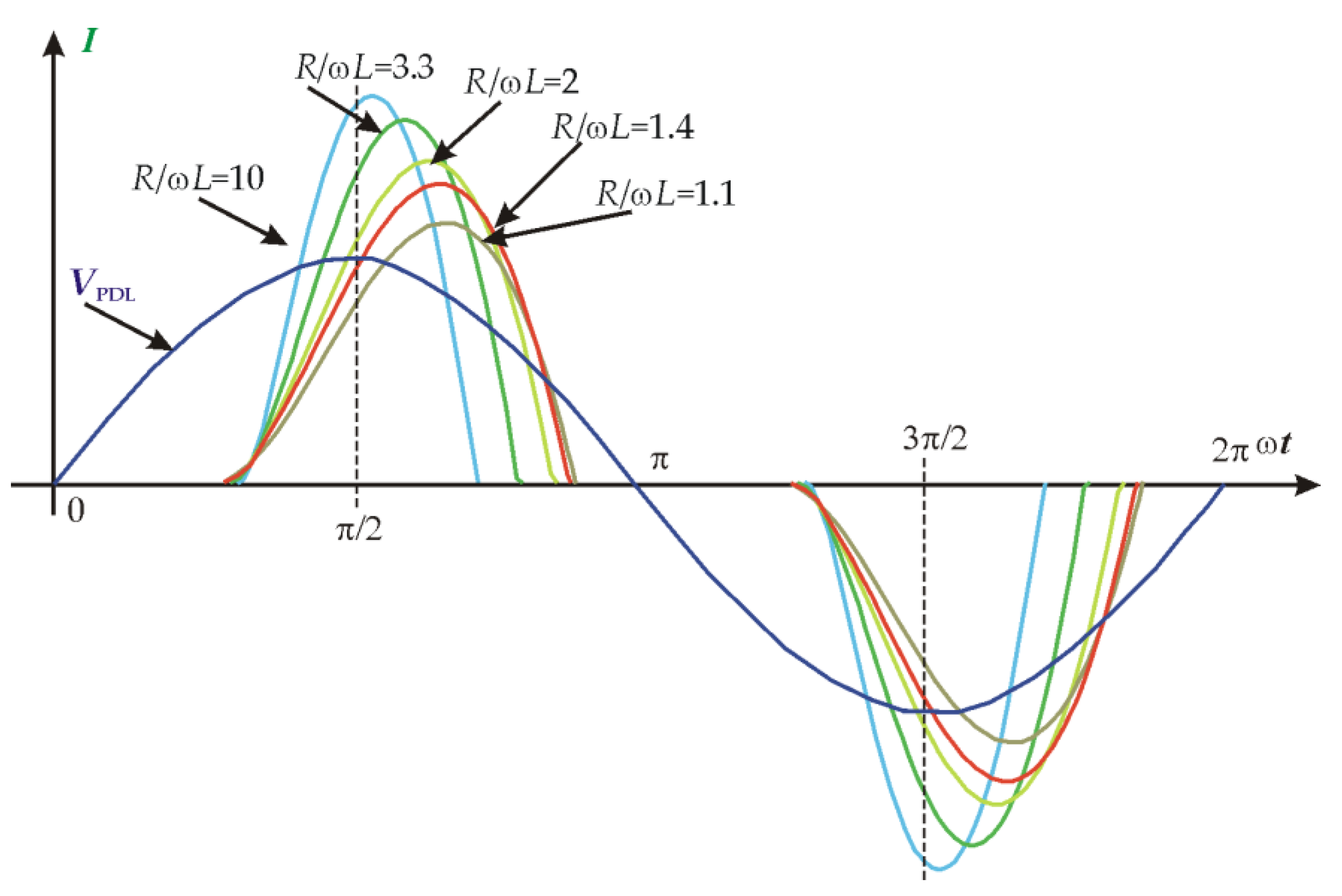
The next step in the analysis of this process is the graphical generation of VFD input current pulse curves in MATLAB and the analysis of the dependence of these curves on the PDL internal R/L ratio.
For the analysis of the influence of the PDL internal R/L ratio, a system with parameters close to those experimentally scanned in the sport arena building and described above was simulated: a value of PLD internal R = 1 Ω, resistance of the circuit consisting of the 1 kW VFD inverter and the induction motor 80 Ω. The internal inductance of the PDL is taken such that the inductive resistance of the PDL is less than or equal to the active resistance, i.e., ωL < 1 Ω. The VFD input current pulse curve generated by MATLAB is decomposed by the Fourier series to determine the angle ϕ1 of displacement of the first harmonic with respect to the sinusoidal voltage PDL. According to this declination, tgϕ1 is obtained, indicating the reactive power QFund of the circuit.
i ( t ) = I 0 + I 1   sin ( ω t + ϕ 1 ) + I 2   sin ( 2 ω t + ϕ 2 )  
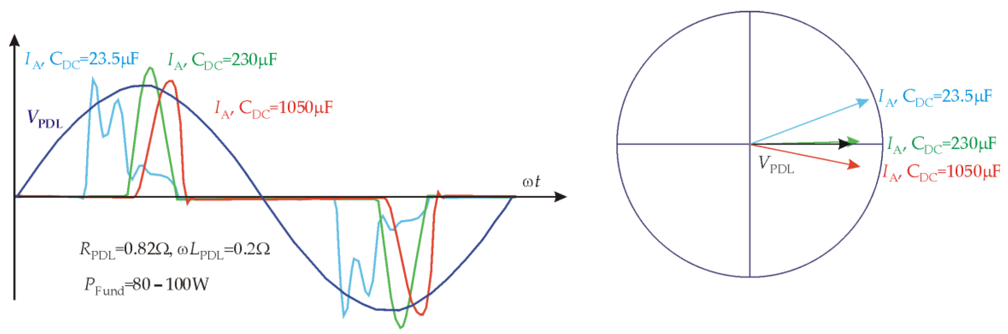
Figure 6 shows the position of the current pulse of one half-period VFD input and the shape of the curve calculated according to Equations (16)–(18). Calculations were performed by varying the value of the internal inductance of the PDL. The position of the curves shows that at the lowest PDL inductance, the impulse of the VFD input current curve is almost symmetrical with respect to the point π/2, so tgϕ and the reactive power QFund are close to zero. This is confirmed by the calculation data in Table 1. Mathematically, only the component i1(t) predominates in this case, and the other component i2(t) is equal to zero. As the internal inductance of the PDL increases, tgϕ increases, thus increasing the i2(t) component and the reactive power drawn out by the VFD. This is evident from the displacement of the VFD input current pulses shown in 
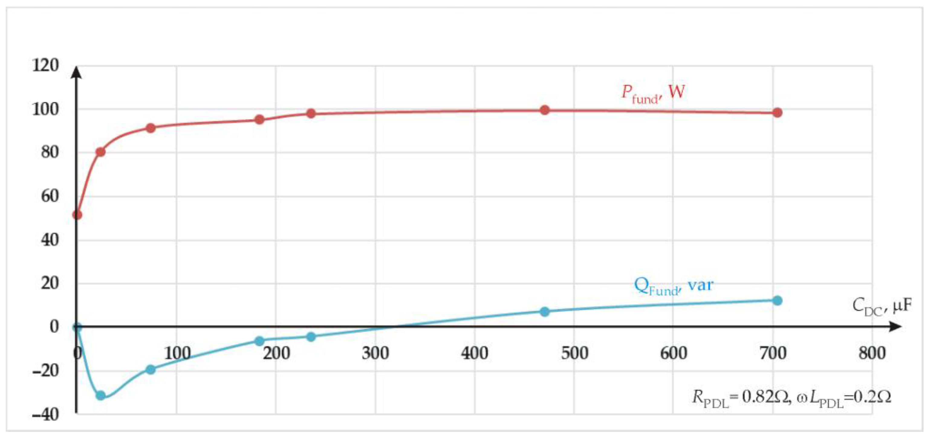
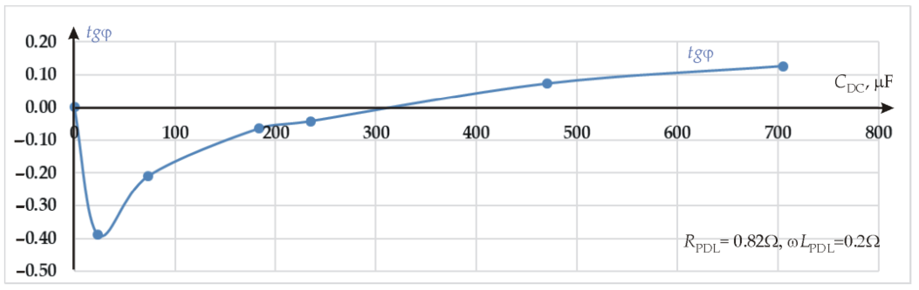
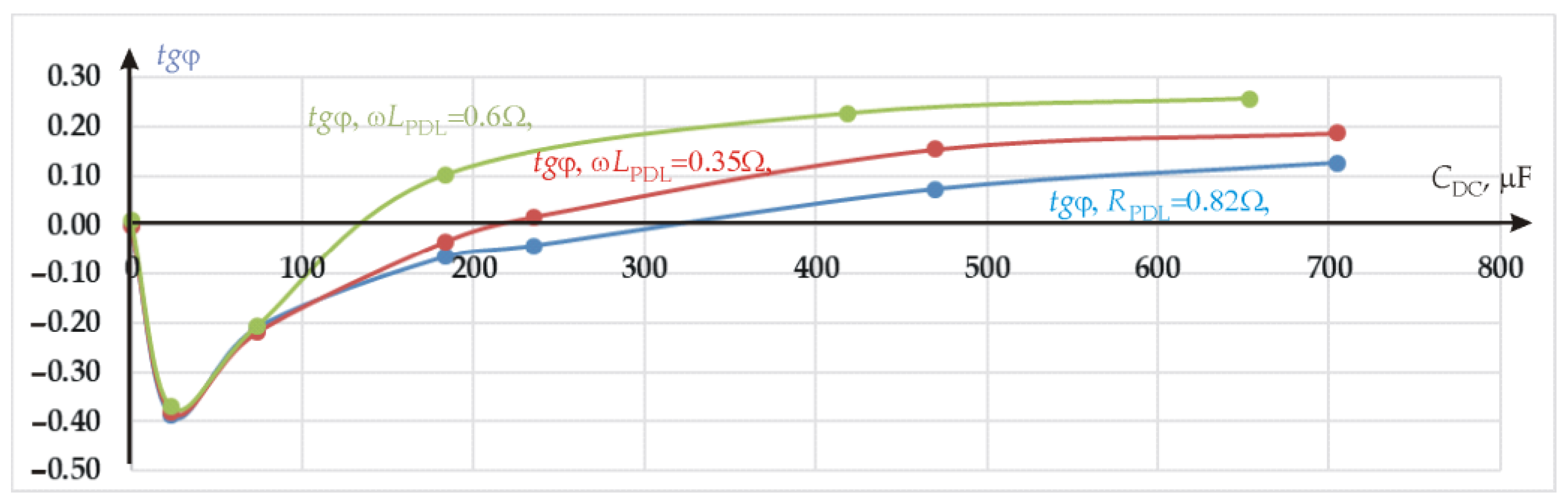
Figure 6 with respect to the PDL voltage. At the maximum values of the internal inductance of the PDL, tgϕ reaches value 0.32, which means that the reactive power provided or drawn out by the VFD is about one-third of the active power of the VFD.
Q Fund = 0.32   P Fund
Another component that can affect the reactive power provided by VFD is the THD reduction inductive choke. The inductive power of this choke is calculated according to the following formula:
Q shunt = I 2 ω L
It is seen that the reactive power of this choke accounts for a small fraction of the reactive power provided or drawn out by the VFD. Thus, using a low-power choke in the input of a series-connected VFD yields a much higher reactive power than traditionally connecting a choke in parallel at the point of connection of the VFD to the PDL. Reactive power compensation by supplementing the VFD DC circuit with electrolytic capacitors is a significantly better method in terms of the price, weight and cost of non-ferrous metals.

2.4. Calculation of DC Circuit Capacitance

The previous calculations were made keeping the capacitor capacity infinite. In a real VFD, which will perform reactive power compensation function in addition to the main functions, real capacity calculations are required. The voltage Uc in the capacitor of the VFD DC circuit can vary only in the small range of ΔUc = 1 ÷ 3%. The equations below are based on the fact that the time interval during which the VFD inverter and the induction motor discharges the capacitor is about Δt = 0.007 s.
Δ Q = C Δ U c
Δ Q = i × Δ t = P 2 Δ t
Comparing the equations gives:
C = P × Δ t 2 × U × Δ U c
The following equation combines the internal resistance of the PDL and the capacitance of the VFD DC circuit. The capacitor must not be fully discharged until the PDL voltage is higher than the VFD DC circuit voltage, thus creating an inequality:
τ = R C t Charge
The pulse displacement angle α of the VFD input current varies within 20 ÷ 30°, so tCharge = 2α =3.3 ms. Assuming a variation of ΔUc of 1 ÷ 3%, it is calculated that the capacity of a 1 kW VFD DC circuit should be between 5500 and 1830 µF. Calculating the time constant TRC at the PDL resistance R = 1 Ω, it is obtained that it varies within 0.0018 s ÷ 0.0055 s. This time constant TRC value is close to the required value.
The calculated VFD DC circuit capacitance values are indicative and will be specified in further experimental studies.

3. Experimental Analysis of the Reactive Power in Nowadays Power Distribution Lines

3.1. Experimental Analysis of the Reactive Power in PDL Loaded by LED Lighting Devices

In order to investigate the reactive power provided by LED light devices, an experiment was performed with the most commonly used LED light bulbs on the Lithuanian market. Different color temperature and different power LED light bulbs were selected. The effect of not only individual LED light bulbs but also their groups on the reactive power of PDL was investigated. The experimental analysis of the reactive power in the LED lighting devices loaded PDL was performed with a METREL MI 2892 power quality analyzer [2].
The experimental setup, for the reactive power provided or drawn out by diode rectifier supply-side device analysis, consists of (Figure A1):
  • Power distribution line connection;
  • METREL MI 2892 power quality analyzer;
  • 806 lm 2700 K LED light bulb;
  • 1850 lm 4000 K LED light bulb;
  • 1500 lm 3000 K LED light bulb;
  • 1350 lm 3000 K LED light bulb;
  • 1350 lm 3000 K LED light bulb;
  • 1055 lm 3000 K.
A photograph of the experimental setup is presented in Figure A2.
The following PDL parameters were investigated:
  • PC—combined active power;
  • NC—combined reactive power;
  • SC—combined apparent power;
  • PF—combined effective power factor;
  • PFund—fundamental harmonic active power;
  • QVFund—fundamental harmonic reactive power;
  • SVFund—fundamental harmonic apparent power;
  • PFVFund—fundamental harmonic displacement factor.
The results of the experimental study are presented in Table 2 and Table 3 and Figure A3, Figure A4, Figure A5 and Figure A6.
The results of this experiment confirm the measurement results reported in publications [15,16]. Despite its excellent lighting properties, LED light devices provide leading reactive power. The total harmonic distortion of the currents taken from their PDL is very high.

3.2. Experimental Analysis of the Reactive Power in PDL Loaded by Diode Rectifier Supply-Side Devices

A photograph of the experimental setup is presented in Figure A7.
The experimental setup, for the reactive power provided or drawn out by diode rectifier supply-side device analysis, consists of (Figure 7):
  • PDL connection switcher;
  • METREL MI 2892 power quality analyzer;
  • Inductive reactor;
  • Diode rectifier;
  • Capacitors bank;
  • DC circuit voltage measuring device;
  • Ohmic load.
The internal parameters of PDL the experimental equipment was connected R = 0.82 Ω, ωL = 0.2 Ω.
The experimentally taken results of power analysis are presented in Figure 8, Figure 9 and Figure 10.
The next step of the experiment was performed by keeping the power constant of the single-phase diode rectifier supply-side device and connecting additional inductive chokes ωLPDL to the PDL circuit. The aim was to increase the reactive power consumption of this diode rectifier supply-side device.
The diagrams in Figure 10 and Figure 11 show that tgϕ reaches 0.25, which confirms the theoretical calculations presented in Table 1 test number 7. It can also be seen that the reactive power changes the character transition from leading to lagging at a DC circuit capacity of 1800 ÷ 4000 μF/kW. This experimental point also confirms the theoretical assumptions. The tgϕ as a function of the DC circuit capacity at different PDL internal resistances and inductances shows that at higher PDL internal inductances, the reactive power of the diode rectifier supply-side device shifts to lagging to a lower DC circuit capacity. The diagrams in Figure 10 correspond in nature to the diagrams in Figure 6 based on theoretical calculations.
As the internal inductance of the PDL increases, the pulse max value of the current flowing to the diode rectifier supply-side device shifts to the lagging power consumption side (Figure 12).
The inductance and resistance of the power distribution lines with the capacitance of the VFD DC circuit form a corresponding resonant frequency with a sequential oscillating circuit. When the instantaneous value of the voltage in the power distribution lines becomes higher than the voltage in the capacitor of the DC circuit, the capacitor charges. Depending on the value of the capacitance in the DC circuit, and the value of the resistance and inductance of the power distribution lines, the charging of the capacitor may occur aperiodic and periodic, with fading oscillations during charging. This is the situation we see in the current waveform at C = 23 µF (Figure 11). With a larger capacity of the DC circuit, charging takes place aperiodically, and the oscillations do not occur, as we see in other current waveforms.

3.3. Experimental Analysis of the Reactive Power in PDL Loaded by LED Light and Diode Rectifier Supply-Side Devices

A photograph of the experimental setup is presented in Figure A8.
The experimental setup, for the reactive power provided or drawn out by LED light and diode rectifier supply-side devices analysis, consists of (Figure 13):
  • PDL connection switcher;
  • METREL MI 2892 power quality analyzer;
  • Diode rectifier;
  • Capacitors bank;
  • DC circuit voltage measuring device;
  • Ohmic load
  • 18 W LED light bulb;
  • 15 W LED light bulb;
  • 15 W LED light bulb;
  • 15 WK LED light bulb.
The experimentally taken results of power analysis are presented in Figure 14.
As can be seen from the diagrams in Figure 14, the reactive power of the PDL depends on the size of the DC circuit capacity of the diode rectifier supply-side device and the number of LED devices connected. By varying the DC circuit capacity value, the diode rectifier supply-side device can fully compensate the reactive power provided by the LED. In this particular experimental case, the size of the capacitors connected in the DC circuit was sufficient to compensate the reactive power provided by the two LEDs (32 W). This is shown in the diagrams in Figure 14a,b. In this case, for two LEDs, increasing the capacity of the DC circuit, the reactive power changed from negative to positive, and there is a point in the diagram where the reactive power is zero and the power factor is equal to one. The phase diagrams in Figure 14a,b show that the current leads against the PDL voltage at the minimum capacitor capacity used (CDC = 23.5 µF). It can also be seen that the current lags behind the PDL voltage at the maximum capacitor capacity (CDC = 1123 µF) used in the experiment. The diagrams in Figure 14c,d show that after connecting the four LED devices (62 W), the maximum DC circuit capacitance used in the experiment is not sufficient to compensate for the reactive power provided by the LEDs. The reactive power remains negative, and the current leads against the PDL voltage.

3.4. Experimental Analysis of the Reactive Power in PDL Loaded by Diode Rectifier Supply-Side Variable Frequency Drive

A photograph of the experimental setup is presented in Figure A9.
The experimental setup, for the reactive power provided or drawn out by diode rectifier supply-side device analysis, consists of (Figure 15):
  • PDL connection switcher;
  • METREL MI 2892 power quality analyzer;
  • Siemens Micromaster 420 variable frequency drive;
  • Induction motor connected to VFD;
  • Mechanically connected to induction motor DC generator;
  • Ammeter for DC generator load current measurement;
  • DC generator loading lamp bulbs;
The aim of this experimental study was to determine the value and type of the reactive power provided or drawn out by a single-phase diode rectifier supply-side VFD. A laboratory workbench with the components described above was used for this purpose. As can be seen from the diagrams in Figure 16, this standard VFD provides leading reactive power over the entire frequency range of the induction motor. It can be argued that standard VFDs, like previously studied LED devices, are the leading sources of reactive power. This study also confirms the data presented in the Section 1, which were obtained experimentally in the sports arena.

4. Application of Single-Phase Supply AC-DC-AC VFD for Power Factor Improvement in LED Lighting Devices Loaded PDL

A photograph of the experimental setup is presented in Figure A10.
The experimental setup, for the reactive power provided or drawn out by diode rectifier supply-side device analysis, consists of (Figure 17):
  • PDL connection switcher;
  • METREL MI 2892 power quality analyzer;
  • SIMOVERT P 6SE21 variable frequency drive;
  • Induction motor powered by the SIMOVERT P 6SE21 VFD;
  • Mechanically connected to induction motor DC generator;
  • Ammeter for DC generator load current measurement;
  • DC generator loading resistors;
  • 18 W LED light bulb;
  • 15 W LED light bulb;
  • 7 W LED light bulb;
  • 15 W LED light bulb;
  • 15 W LED light bulb;
  • DC circuit voltage measuring device;
  • Capacitors bank;
  • Resistor for capacitors discharging.

4.1. The Reactive Power in PDL Loaded by SIMOVERT P 6SE21 VFD

The SIMOVERT P 6SE21 VFD is factory-fitted with a relatively high-capacity DC circuit capacitor—470 μF. Therefore, this VFD, unlike the VFDs studied in Section 3.4 and presented in [4], provides leading reactive power only at the maximum high induction motor voltage frequency (67–80 Hz). However, by connecting additional capacitors to the SIMOVERT P 6SE21VFD DC circuit, the reactive power provided or drawn out by the VFD becomes lagging over the entire frequency range of the induction motor voltage. This is clearly seen in the diagrams in Figure 18a.
The results of the experiment show that with natural PDL internal resistance and inductance and a factory-fitted DC circuit capacitor, the VFD consumes lagging active power only up to a certain load level. By increasing the load on the VFD above this level, the VFD begins to provide leading reactive power. In order for the VFD to remain a consumer of lagging reactive power and to be able to compensate the leading reactive power provided by the LED, the capacitance of the DC circuit capacitors must be increased. In addition, an experiment with SIMOVERT P 6SE21VFD showed that the additional capacitors in the DC circuit have no real effect on the active power.

4.2. Compensation of Reactive Power Provided by LED Light Devices by SIMOVERT P 6SE21 VFD Fitted by Additional Capacitance in DC Circuit

This experimental study was performed to test the ability of SIMOVERT P 6SE21VFD to compensate for the reactive power provided by LED light devices. According to the study described in Section 3.1, all experimentally investigated LED light devices provide leading reactive power. This is confirmed by the data published in [2]. According to the results of the study described in Section 4.1, additional capacitors in the VFD DC circuit convert the VFD into a lagging reactive power source. It was assumed that the reactive power provided by the LED light devices connected to the PDL would have to be compensated by the aforementioned VFD. This assumption was tested experimentally. The study was performed by connecting five different power and color temperature LED light devices and SIMOVERT P 6SE21VFD to PDL. Data were collected at the point of connection of these devices to the PDL. The results of the experimental study are presented in Figure 19.
As can be seen from the results of the experimental study in Figure 19a, using the SIMOVERT P 6SE21 VFD only with a factory-fitted 470 mF capacitor, we have the leading reactive power over the entire frequency range of the induction motor voltage. With the factory-fitted 470 mF capacitor, the SIMOVERT P 6SE21 VFD does not compensate the reactive power provided by the LED. By connecting additional capacitors in the VFD DC circuit and increasing the capacity to 705 µF, the SIMOVERT P 6SE21 VFD becomes able to compensate the reactive power provided by the LED in the frequency range between 30 and 70 Hz. However, it is not capable of the remaining frequency range. By connecting additional capacitors to the VFD DC circuit and increasing the capacity to 815 µF, the SIMOVERT P 6SE21 VFD becomes able to compensate the reactive power provided by the LED over the entire voltage frequency range of the induction motor.
It is also found that the additional capacitors in the SIMOVERT P 6SE21 VFD DC circuit do not affect the active power. As can be seen from the data in Figure 18b and Figure 19b, the active power remains the same at all capacitances of the DC circuit of the VFD, and the VFD acquires the ability to operate as a reactive power compensator.

5. Discussion

The need to find ways to compensate the leading reactive power provided by LED light devices has arisen due to the problems created by these light devices being connected to the conventional type of power distribution lines. These problems are due to the overcompensation of reactive power when LED lighting devices and capacitor-based compensating devices interact. Consumers pay fines to electricity supply companies for this overcompensation. Therefore, ways have been sought to compensate this reactive power with the available means and with the least possible investment. One of the easily accessible means is a large number of VFDs connected to the same power distribution lines as LEDs.
In this study, it has been shown mathematically and experimentally that most diode rectifier supply-side devices, including conventional AC-DC-AC VFDs, provide leading reactive power. It has also been shown mathematically and experimentally that by varying the capacitance of DC circuit capacitors, the value and type of reactive power can be varied—transfer from leading reactive power to lagging. In this way, these conventional VFDs acquire the ability not only to perform their main functions—motor powering and speed control, but also to perform the functions of a reactive power compensator.
In this study, it has been mathematically shown that the ability of a VFD to consume reactive power is related to the interaction between the capacitance of the VFD DC circuit and the internal inductance of the power distribution lines, or to the inductance of the additional choke. As a result of this interaction, the VFD consumes many times more reactive power compared to the reactivity of the inductance of the power distribution lines or the inductance of the auxiliary choke.
The experiment connecting a group of LED light devices and conventional VFD with additional DC circuit capacitors to the same power distribution line showed that such VFD can compensate the reactive power provided by LEDs.
Despite the advantages listed, this method of reactive power compensation has a number of practical limitations. The control of power factor is not continuous but gradual. The method requires access to the intermediate DC circuit of the VFD. Not all VFD manufacturers allow it, especially during the warranty period.
Despite the relatively high power of LED loads, only single-phase power distribution lines and single-phase supply side VFDs are considered in this study. This is due to the fact that most of the VFDs installed in the observed sports arena are single-phase. They are used to power and control the motors of pumps, fans and other engineering equipment. Therefore, a single-phase supply VFD is investigated in this study. The application of three-phase VFD to reactive power compensation is planned in further studies.
The aim of this study is to show a possible way to compensate the reactive power of LEDs. Therefore, in these experiments, additional capacitors in the VFD DC circuit were connected manually using circuit breakers. Using such compensation in practice, an additional unit with capacitors, their switching electronic switches and a controller should be constructed. It will be the subject of future work.

Author Contributions

Conceptualization, G.S.; methodology, G.S.; software, G.P.; validation, G.S. and G.P.; formal analysis, G.S.; investigation, G.P. and G.S.; resources, G.P. and G.S.; writing—original draft preparation, G.P.; writing—review and editing, G.S.; visualization, G.P.; funding acquisition, G.P. All authors have read and agreed to the published version of the manuscript.

Funding

This research was supported by the Lithuanian Agency for Science, Innovation and Technology [grant number MITA-T-851-01-0032].

Institutional Review Board Statement

Not applicable.

Informed Consent Statement

Not applicable.

Data Availability Statement

Not applicable.

Conflicts of Interest

The authors declare no conflict of interest.

Appendix A

Matlab codes for calculating displacement using Fourier series.
%calculation rectifier input current
clear all;
%initial parameters: angle, network resistance, resistance-inductance relatioship
fi = 27; R = 1; Rapk = 80; t = 0; Um = 300; w = 314; L = 0.0032/10 * 10;g = R/L;Q = 0;
gal = 100;
%circle of current calculation according Duhamel integral
for kam = 0:gal
t = kam * 0.02/360; dt = 0.02/360;
%calculation current value according derived equations
i1 = (sin((w * t + 90/57.2 − fi/57.2)) − sin((90/57.2 − fi/57.2)))/w;
i2 = (cos(w * t + 90/57.2 − fi/57.2) * g + sin(w * t + 90/57.2 − fi/57.2) * w)/(g^2 + w^2);
i3 = −exp(−g * t) * (cos(90/57.2 − fi/57.2) * g + sin(90/57.2 − fi/57.2) * w)/(g^2 + w^2);
it = Um * w * (i1-i2-i3)/(R);
% if current less zero canceling calculation
if it < 0;
it = 0;
end;
srov(kam + 1) = it;
%calculation electric charge of input current
Q = Q + it * dt;
end
Qik = Q
Uc = Um * sin((90/57.2 − fi/57.2));
%calculation electric charge of output current
Qisk = Uc/Rapk * 0.01
Uc
P = Uc^2/Rapk
%Full period data formation from calculated current and zeros
srove(1:90 − fi) = 0;
srove1 = [srove srov];
ik = max(size(srove1));
srove1(ik + 1:180) = 0;
%current plol
plot(srove1)
%current mean square value
kvadrsr = sum(srove1.^2) * 2/360;
kvadr = sqrt(kvadrsr);
Reakt = kvadr^2 * w * L
% Fourier series calculation; x-one current period input data; num-number of harmonic;
% a first colume-harmonic amplitude; a second colume-harmonic phases.
num = 11;
x = [srove1 − srove1];
n = max(size(x));
eil = linspace(2 * pi/n,2 * pi,n);
har = round(n)/2;
a(1,1) = sum(x)/n;a(1,2) = 0;b(1) = a(1,1);
for i = 1:num;
tarp = x.* sin(i * eil);
tarp1 = x.*cos(i * eil);
sk = sum(tarp) * 2/n;
is = sum(tarp1) * 2/n;
a(i + 1,1) = sqrt((sk * sk)+(is * is));b(i + 1) = a(i + 1,1);
a(i + 1,2) = atan(is/sk);
end;
knes = sqrt(sum(b(3:num + 1).* b(3:num + 1))) * 100/b(2);
%output parameters – first harmonic phase displacement angle(degrees) and tan of angle
poslinkis = a(2,2) * 57.1
tangentas = tan(a(2,2))

Appendix B

Figure A1. Circuit diagram of experimental setup for the reactive power provided by LED devices analysis.
Applsci 12 05955 g0a1
Figure A2. Photo of experimental setup for the reactive power provided by LED devices analysis.
Applsci 12 05955 g0a2
Figure A3. Experimental measurements at the point of connection 806 lm 2700 K LED light bulb to PDL: (a) Voltage and current time diagrams; (b) Voltage and current phase diagrams defined for first harmonic.
Applsci 12 05955 g0a3
Figure A4. Experimental measurements at the point of connection 1850 lm 4000 K LED light bulb to PDL: (a) Voltage and current time diagrams; (b) Voltage and current phase diagrams defined for first harmonic.
Applsci 12 05955 g0a4
Figure A5. Experimental measurements at the point of connection 1500 lm 3000 K LED light bulb to power distribution lines: (a) Voltage and current time diagrams; (b) Voltage and current phase diagrams defined for first harmonic.
Applsci 12 05955 g0a5
Figure A6. Experimental measurements at the point of connection 1350 lm 3000 K LED light bulb to PDL: (a) Voltage and current time diagrams; (b) Voltage and current phase diagrams defined for first harmonic.
Applsci 12 05955 g0a6
Figure A7. Photo of experimental setup for the reactive power provided or drawn out by diode rectifier supply-side device analysis.
Applsci 12 05955 g0a7
Figure A8. Photo of experimental setup for the reactive power provided or drawn out by LED light and diode rectifier supply-side devices analysis.
Applsci 12 05955 g0a8
Figure A9. Photo of experimental setup for the reactive power provided or drawn out by Siemens Micromaster 420 single-phase diode rectifier supply-side VFD analysis.
Applsci 12 05955 g0a9
Figure A10. Photo of experimental setup for the reactive power provided or drawn out by diode rectifier supply-side variable frequency drive and LED light devices analysis.
Applsci 12 05955 g0a10

References

  1. Lamar, D.G. Latest Developments in LED Drivers. Electronics 2020, 9, 619. [Google Scholar] [CrossRef]
  2. Petrauskas, G.; Svinkunas, G. Application of Matrix VFD for Power Factor Improvement in LED Lighting Sources Loaded Power Distribution Lines. Energies 2021, 14, 3546. [Google Scholar] [CrossRef]
  3. Coman, C.M.; Florescu, A.; Oancea, C.D. Improving the Efficiency and Sustainability of Power Systems Using Distributed Power Factor Correction Methods. Sustainability 2020, 12, 3134. [Google Scholar] [CrossRef]
  4. Petrauskas, G.; Svinkunas, G.; Jonaitis, A.; Giannakis, A. Application of Novel AC–AC Matrix VFD for Power Factor Improvement in Conventional AC–DC–AC VFD-Loaded Power Distribution Lines. Electronics 2022, 11, 997. [Google Scholar] [CrossRef]
  5. Zieliński, D.; Stefańczak, B.; Jędrys, K. Phase-Independent Reactive Power Compensation Based on Four-Wire Power Converter in the Presence of Angular Asymmetry between Voltage Vectors. Energies 2022, 15, 497. [Google Scholar] [CrossRef]
  6. Wang, X.; Dai, K.; Chen, X.; Zhang, X.; Wu, Q.; Dai, Z. Reactive Power Compensation and Imbalance Suppression by Star-Connected Buck-Type D-CAP. Energies 2019, 12, 1914. [Google Scholar] [CrossRef]
  7. Petrushyn, V.; Horoshko, V.; Plotkin, J.; Almuratova, N.; Toigozhinova, Z. Power Balance and Power Factors of Distorted Electrical Systems and Variable Speed Asynchronous Electric Drives. Electronics 2021, 10, 1676. [Google Scholar] [CrossRef]
  8. Cheng, C.-A.; Chang, C.-H.; Cheng, H.-L.; Chang, E.-C.; Chung, T.-Y.; Chang, M.-T. A Single-Stage LED Streetlight Driver with Soft-Switching and Interleaved PFC Features. Electronics 2019, 8, 911. [Google Scholar] [CrossRef]
  9. Tung, N.T.; Tuyen, N.D.; Huy, N.M.; Phong, N.H.; Cuong, N.C.; Phuong, L.M. Design and Implementation of 150 W AC/DC LED Driver with Unity Power Factor, Low THD, and Dimming Capability. Electronics 2020, 9, 52. [Google Scholar] [CrossRef]
  10. Yan, Y.-H.; Cheng, H.-L.; Cheng, C.-A.; Chang, Y.-N.; Wu, Z.-X. A Novel Single-Switch Single-Stage LED Driver with Power Factor Correction and Current Balancing Capability. Electronics 2021, 10, 1340. [Google Scholar] [CrossRef]
  11. Cano Ortega, A.; Sánchez Sutil, F.J.; De la Casa Hernández, J. Power Factor Compensation Using Teaching Learning Based Optimization and Monitoring System by Cloud Data Logger. Sensors 2019, 19, 2172. [Google Scholar] [CrossRef] [PubMed]
  12. Dixon, J.; Morán, L.; Rodríguez, J.; Domke, R. Reactive power compensation technologies: State-of-the-art review. Proc. IEEE 2005, 93, 2144–2164. [Google Scholar] [CrossRef]
  13. Júniora, H.G.; Liberadob, E.V.; Pomilioa, J.A.; Marafãob, F.P. General-compensation purpose Static Var Compensator Prototype. Hardware X 2018, 5, e00049. [Google Scholar] [CrossRef]
  14. De Siqueira, J.C.G.; Bonatto, B.D. Introduction to Transients in Electrical Circuits–Analytical and Digital Circuits; Springer International Publishing: Berlin/Heidelberg, Germany, 2021. [Google Scholar]
  15. Wlas, M.; Galla, S. The Influence of LED Lighting Sources on the Nature of Power Factor. Energies 2018, 11, 1479. [Google Scholar] [CrossRef]
  16. Sikora, R.; Markiewicz, P. Analysis of Electric Power Quantities of Road LED Luminaires under Sinusoidal and Non-Sinusoidal Conditions. Energies 2019, 12, 1109. [Google Scholar] [CrossRef]
Figure 1. The 32 kW LED wall display at a sports arena: (a) Installation of the wall display; (b) Time diagram of active and reactive power at the point of LED wall display connection to 0.4 kV power distribution line.
Applsci 12 05955 g001
Figure 2. The loads and compensation device of the 0.4 kV power distribution lines: (a) Conventional load of power distribution lines; (b) Modern load of power distribution lines (causes overcompensation).
Applsci 12 05955 g002
Figure 3. Proposed modernization of the conventional single-phase supply AC-DC-AC VFD for the reactive power compensation in LED-loaded power distribution lines.
Applsci 12 05955 g003
Figure 4. Operation modes of VFD from point of view of the input reactive power [2]: (a) leading; (b) zero; (c) lagging.
Applsci 12 05955 g004
Figure 5. Calculation of the transient process: (a) voltages; (b) equivalent circuit.
Applsci 12 05955 g005
Figure 6. VFD input current pulse i(t) position at different PDL internal R/ωL ratios calculated on the basis of Equations (16)–(18).
Applsci 12 05955 g006
Figure 7. Circuit diagram of experimental setup for the reactive power provided or drawn out by diode rectifier supply-side device analysis.
Applsci 12 05955 g007
Figure 8. Active and reactive power components at the point of connection of the single-phase diode rectifier supply-side device to the PDL as a function of DC circuit capacity value in case of internal parameters of PDL-connected R = 0.82 Ω, ωL = 0.2 Ω.
Applsci 12 05955 g008
Figure 9. tgϕ at the point of connection of the single-phase diode rectifier supply-side device to the PDL as a function of DC circuit capacity value, in case of internal parameters of PDL-connected RPDL = 0.82 Ω, ωLPDL = 0.2 Ω.
Applsci 12 05955 g009
Figure 10. tgϕ at the point of connection of the single-phase diode rectifier supply-side device to the PDL as a function of DC circuit capacity value in case of different PDL inductivity and resistance.
Applsci 12 05955 g010
Figure 11. Time and phase diagrams of the current at the point of connection of single-phase diode rectifier supply-side device to the PDL in the case of different DC capacitance value.
Applsci 12 05955 g011
Figure 12. Time and phase diagrams of the current at the point of connection of single-phase diode rectifier supply-side device to the PDL in the case of different PDL internal resistance and inductivity.
Applsci 12 05955 g012
Figure 13. Circuit diagram of experimental setup for the reactive power provided or drawn out by LED light and diode rectifier supply-side devices analysis.
Applsci 12 05955 g013
Figure 14. Active and reactive power provided or drawn out by LED light and diode rectifier supply-side devices as function of DC circuit capacity value: (a) 15 W LED light bulb, (b) 32 W light bulbs; (c) 48 W LED light bulbs; (d) 62 W LED light bulbs.
Applsci 12 05955 g014
Figure 15. Circuit diagram of experimental setup for the reactive power provided or drawn out by Siemens Micromaster 420 single-phase diode rectifier supply-side VFD analysis.
Applsci 12 05955 g015
Figure 16. Active and reactive power provided or drawn out by Siemens Micromaster 420 single-phase diode rectifier supply-side VFD as a function of VFD frequency.
Applsci 12 05955 g016
Figure 17. Circuit diagram of experimental setup for the reactive power provided or drawn out by diode rectifier supply-side variable frequency drive and LED light devices analysis.
Applsci 12 05955 g017
Figure 18. The power at the point of SIMOVERT P 6SE21 VFD connection to PDL at a function of induction motor frequency in case of different DC circuit capacitance value: (a) reactive power; (b) active power.
Applsci 12 05955 g018
Figure 19. The power at the point of SIMOVERT P 6SE21 VFD and five different type of LED lighting devices connection to PDL at a function of induction motor frequency in case of different DC circuit capacitance value: (a) reactive power; (b) active power.
Applsci 12 05955 g019aApplsci 12 05955 g019b
Table 1. Electrical parameters at the point of connection of the VFD to the PDL and their dependence on the internal R/ωL ratio of the PDL.
Test NumberωL, Ωα, °Uc, VP, WQShunt, varϕ, °tgϕR/ωL
10.1222789685−5.5−0.09710.0
20.22327695410−8.5−0.155.0
30.32427594016−10.6−0.183.3
40.42427493517−12.0−0.212.5
50.52527292522−13.4−0.242.0
60.62626991029−14.6−0.261.7
70.72726789436−15.7−0.281.4
80.82726789038−16.3−0.291.3
90.92826688540−16.9−0.301.1
1012826587843−17.8−0.321.0
Table 2. The electrical parameters of the LED light bulbs at the point of connection to the PDL.
No.LED Bulb TypePC, WNC, varSC, VAPFQVFund, varSVFund, VAtanϕFundPFVFund
17 W 806 lm 2700 K5.18−14.515.40.966−1.45.55−0.2770.952
215 W 1850 lm 4000 K15.9−26.1230.60.912−7.2717.8−0.4560.912
315 W 1500 lm 3000 K13.32−23.326.80.867−7.715.5−0.5790.867
415 W 1350 lm 3000 K12.6−27.0529.80.945−4.4313.6−0.3530.943
Table 3. The electrical parameters of the LED light bulbs combination connected to the PDL.
No.No. of LED Bulb ConnectedPC, WNC, varSC, VAPFQVFund, varSVFund, VAtanϕFundPFVFund
1 and 221.9−36.742.80.937−8.30723.8−0.3780.937
1 and 2 and 336−56.6670.921−15.539.8−0.430.921
1 and 2 and 3 and 449.7−72.780.080.938−18.753.9−0.3670.938
Publisher’s Note: MDPI stays neutral with regard to jurisdictional claims in published maps and institutional affiliations.

