
Mitigation of Electro Magnetic Interference by Using C-Shaped Composite Cylindrical Device


1
Department of Computer Science and Information Engineering, Asia University, Taichung 41354, Taiwan
2
Department of Bioinformatics and Medical Engineering, Asia University, Taichung 41354, Taiwan
3
Department of Civil Engineering, National Taiwan University, Taipei 10617, Taiwan
*
Author to whom correspondence should be addressed.
Appl. Sci. 2022, 12(2), 882; https://0-doi-org.brum.beds.ac.uk/10.3390/app12020882
Submission received: 7 November 2021
/
Revised: 12 January 2022
/
Accepted: 14 January 2022
/
Published: 16 January 2022
(This article belongs to the Special Issue Advanced Technologies in Electromagnetic Compatibility)
Abstract
:The extremely low-frequency (ELF) and its corresponding electromagnetic field influences the yield of CMOS processes in the foundry, especially for high-end equipment such as scanning electron microscopy (SEM) systems, transmission electron microscopy (TEM) systems, focused ion beam (FIB) systems, and electron beam lithography (E-Beam) systems. There are several techniques to mitigate electromagnetic interference (EMI), among which active shielding systems and passive shielding methods are widely used. An active shielding system is used to generate an internal electromagnetic field to reduce the detected external electromagnetic field in electric coils with the help of the current. Although the active shielding system reduces the EMI impact, it induces an internal electromagnetic field that could affect the function of nearby tools and/or high-performance probes. Therefore, in this study, we have used a C-shaped cylindrical device combined with an active shielding system and passive shielding techniques to reduce EMI for online monitoring and to overcome the aforementioned issues. In this study, the active shielding system was wrapped with a permalloy composite material (i.e., a composite of nickel and iron alloy) as a tubular device. A C-shaped opening was made on the tubular structure vertically or horizontally to guide the propagation of the electromagnetic field. This C-shaped cylindrical device further reduced electromagnetic noise up to −5.06 dB and redirected the electromagnetic field toward the opening direction on the cylindrical device. The results demonstrated a practical reduction of the electromagnetic field.
1. Introduction
With the evolution of the semiconductor foundry, the gate/line width of the process has been getting smaller for a higher-density integrated circuit. Since various electrical high-power cables are used in the foundry and every electronic tool generates associated extremely low-frequency (ELF) electromagnetic fields according to its input electricity, it indispensably causes ELF electromagnetic fields generally below 300 Hz [1,2,3]. This ELF keeps the production capacity away from its original designed pattern or layouts. Especially, electronic fine tools including scanning electron microscopy (SEM) systems, transmission electron microscopy (TEM) systems, focused ion beam (FIB) systems, and electron beam lithography (E-Beam) systems are very susceptible to ELF magnetic fields [3,4,5]. This misoperation happens because of ELF magnetic fields inducing the beam shift during the measurement or process for cutting-edge chips below the 40-nanometer process. The international technology roadmap for semiconductors recommended that the maximum field strength is 0.3 mG for electromagnetic interference (EMI) [6,7,8,9,10]. The definition of EMI-sensitive equipment is any equipment with a performance that is adversely affected by EMI present in the semiconductor-manufacturing environment. The user that acquires equipment to manufacture semiconductors equipment should perform an ELF and EMF audit before installing semiconductor manufacturing equipment to determine if the areas are compatible with the equipment’s immunity limits to prevent having to relocate equipment due to interference generated by the facility infrastructure or other equipment [11]. After installing semiconductor manufacturing equipment, the user should perform an ELF and EMF audit again to determine if the areas are still compatible with the semiconductor-manufacturing equipment EMI immunity limits and that the equipment itself does not generate ELF EMFs to prevent interference with other nearby ELF-sensitive equipment. In addition, every tool or instrument that uses electricity generates associated electromagnetic fields. It might be ELF. For example, a 10-nanometer offset can be observed, if electron beams work with an acceleration voltage of 300 V under EMI with a field strength of 1 mG [12].
In general, there are two methods to reduce EMI, including the active shielding method and the passive shielding method [13,14,15,16,17,18]. The passive shielding is to build an electromagnetic-free chamber for protecting delicate equipment. The appropriate materials are sheets of Mu-metal or permalloy. They have excellent shielding properties to absorb or reflect electromagnetic fields [19,20]. The propagation of electromagnetic waves thus has an impedance discontinuity on the propagation path. The major drawback of the passive shielding method is that it is expensive and also inconvenient for large-scale coverage [21]. The active shielding method uses coils with a current-sensing field with a sensor and induces a man-made electromagnetic field to reduce the stray magnetic field. Upon data processing, the processor sends a signal which responds to the amplitude of the convertor for counteracting the outcoming electromagnetic field [22,23]. The convertor immediately delivers a current to the electric coils which produces a corresponding anti-electromagnetic wave to counteract the sensed electromagnetic wave. Even the active shielding coils are strapped only to the frame of EMI-sensitive equipment; the disadvantage of the active shielding method is that it may be a new source of EMI [24]. Thus, it is necessary to develop better shielding devices for the irresistible ELF and EMI.
The most practical way to increase the shielding effectiveness (SE) is the improvement of absorption loss [25]. It is well-known that high-permeability materials such as permalloy materials have an excellent shielding capability [26]. On the other hand, current-carrying electric coils certainly establish an electromagnetic field around itself [27]. If the electromagnetic field from the source can be minimized, the maximum SE for the productivity of high-performance tools could be achieved. Therefore, in this study, the passive shielding method was combined with the active shielding methodology to mitigate the electromagnetic fields on the target space with a higher efficiency by wrapping passive shielding materials with a C-shaped cylindrical device around the coils of the active shielding system. In this study, the tubular structure was suggested to collect all electromagnetic fields around power cable lines. Presumably, the C-shaped cylindrical structure with high-permeability materials emits an electromagnetic field to the opening space for a better shielding design [28,29]. A similar shape effect can be observed in U-type barium hexaferrite-epoxy composites [30] and hollow conducting tubes [31].
2. Experimental and Simulation Setup
Nowadays, the high-tech industry is one of the important developments across the globe. A good working environment is essential for precision production technology. High-tech plant’s location, structure, detail design, and clean room rely on civil engineer careful planning. With the evolution of the process technology, the gate width of the process has been getting smaller and smaller. The number of the requirements for cleanroom are being increased, so enhancing the level of the semiconductor plant is also an important issue for a civil engineer.
In the past, the concern of the plant ecology has been focused on cleaning cells in the air. Today, micro-vibrations, organic and inorganic chemical pollutants, and EMI in the plant have some requirements. For example, EMI becomes more vulnerable to electron microscopy equipment used in 28 nm processes such as SEM, TEM, FIB, and E-Beam systems. If this device is affected by a magnetic field of 100 nT when electron beams are operating with a velocity voltage of 300 V, then there will be an error of 10 nm. That means the EMI issue will continue to be discussed. Production equipment is often an expensive machine if combined with electromagnetic fields, which greatly reduces its production capacity.
2.1. Materials
A high-permeability material and a permalloy material were purchased from Starek Scientific Co., Ltd. and used as received without further treatment [9]. In Figure 1, the radius and the length of the high-permeability material were 1.25 cm and 50 cm, respectively. The thicknesses of the high-permeability material and the permalloy pipe were 0.20 cm, and the width of the C-shaped opening gap was ~0.05 cm.
2.2. Preparation of the C-Shape Composite Device
The C-shaped cylindrical device combined with the passive shielding method and the active shielding method was used to counteract the environmental electromagnetic field. The device structure was made by using an electric coil surrounded by an electromagnetic-shielding material. A high-permeability material and a permalloy material that absorbed the majority of electromagnetic waves were used for electromagnetic shielding. Electric coils served as the active shielding system, depending on the input current. The C-shaped opening was cut by a wire-cutting machine for the perfect edge. For a C-shaped device, it was expected that C-shape could gather magnetic field lines around it and emit magnetic field lines to the opening. With such a lens, the magnetic field lines were collected by the C-shape with a high-permeability material and emitted through the focus.
2.3. Characterization
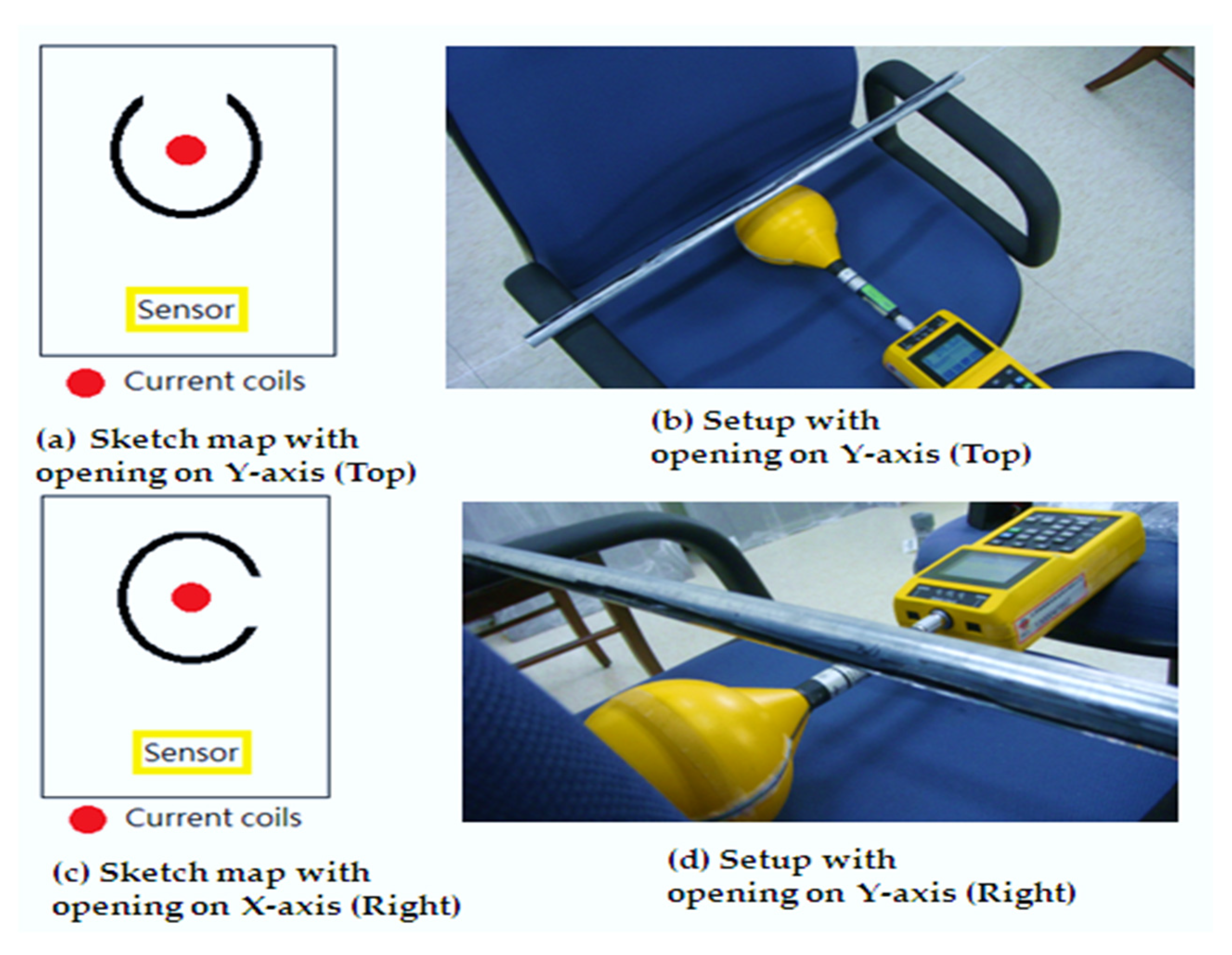
A field meter was applied to detect electromagnetic waves. It was purchased from Chauvin Arnoux Co., Ltd., Dewsbury, England with serial no. 100539GHK. An internal isotropic-magnetic-field probe scanned electromagnetic waves from 10 Hz to 30 kHz and from 200 nT to 40 mT. The measurements were carefully calibrated before experiments. For example, the distance between the sensor and the C-shaped high-permeability material was 7 cm, as shown in Figure 1. The realistic experimental setup can be observed in Supporting Information Materials. In Figure 2, the measurement depended on the distance in the experiments.
3. Results and Discussion
3.1. Simulation
MagNet is one of the low-frequency electromagnetic field simulation software. It can rapidly model and predict the performance of electromagnetic or electro-mechanical devices. Its solver is based on the finite element method for simulating static, frequency-dependent, or time-varying electromagnetic fields. The setup parameters of the C-shaped device simulation are shown as follows: The length of the conducting wire was 200 m (the Z-axis, from −100 m to 100 m) with the boundary condition of −1 m to 1 m in the Z-axis. The angle of the C-shaped opening was 90° aligned at the horizontal plane with a radius of 3 cm. Mu-metal was selected as the C-shaped composite device material from MagNet’s database. The operating frequency was 60 Hz with an electric current of 1 A. As shown in Figure 2a–c, the tubular structure of the high-permeability material shielded the electromagnetic field effectively, and the value was the root mean square. It was obvious that the opening far away sensor could shield from EMF and enhance the opening-sided EMF. The results showed the evidence that a C-shaped device with a high-permeability material can collect magnetic field lines and emit them from the opening. As the electromagnetic field decayed rapidly with the distance, the reinforcement of the C-shaped device was not obvious, because the electric current in this study was 1 A.
In contrast, the electromagnetic field emitted from the opening in the X-axis, while the C-shaped opening was aligned on the horizontal plane. In Figure 2c and Table 1, the shielding efficiency was −0.085 dB at the least and −0.40 dB at most according to the distance of EMI measurements. The efficiency was calculated by the ratio of the “tubular structure opening (T)” and the “C-shaped opening (C)”:
The negative efficiency indicated that the tubular composite device protected the electromagnetic field, while the positive capacitance indicated that the C-shaped structure increased the electromagnetic field in the aperture vector. Although the electromagnetic field decreased rapidly with the distance, the EMI improvement of the C-shaped aperture still was shown to some degree. This is due to the C-shaped open position and the low voltage across the electrical coils.
3.2. Monitoring of Electromagnetic Fields
The cases of the C-shape high-permeability material and the permalloy material were set to confirm that whether the opening direction of the C-shaped cylindrical device interfered with the measured electromagnetic fields. Several voltages at a frequency of 60 Hz were applied in the coils, and the electromagnetic background was 0.3 mG. The peak values were recorded for the tubular structure, the vertical (i.e., the Y-axis) opening, and the horizontal (i.e., the X-axis) opening on the high-permeability material. The detailed experimental results are listed in Table 2. It is noted that the opening in the horizontal direction of the high-permeability material shielded electromagnetic fields above 1 dB. The opening in the vertical direction of the high-permeability material shielded the electromagnetic field below 1 dB, because of the collinear with the C-shaped opening. Figure 3a–b and Figure 4 demonstrate the comparison of the measured electromagnetic fields from the tubular structure without an opening and the C-shaped cylindrical devices with an opening in the Y-axis (top) and an opening in the X-axis (right). The results suggested that the emission of electromagnetic fields could be directive according to the C-shaped opening position.
Further, the high-permeability material and the permalloy material were used to confirm the shielding efficiency of the C-shaped cylindrical device. The electric current coil was wrapped into the center of the tubular permalloy structure and its corresponding C-shaped cylindrical device. A voltage of 1.43 V with a current of 0.6 A at a frequency of 60 Hz was applied in the coil, while the electromagnetic background was 0.3 mG. The peak value was recorded for the horizontal opening on the permalloy pipe.
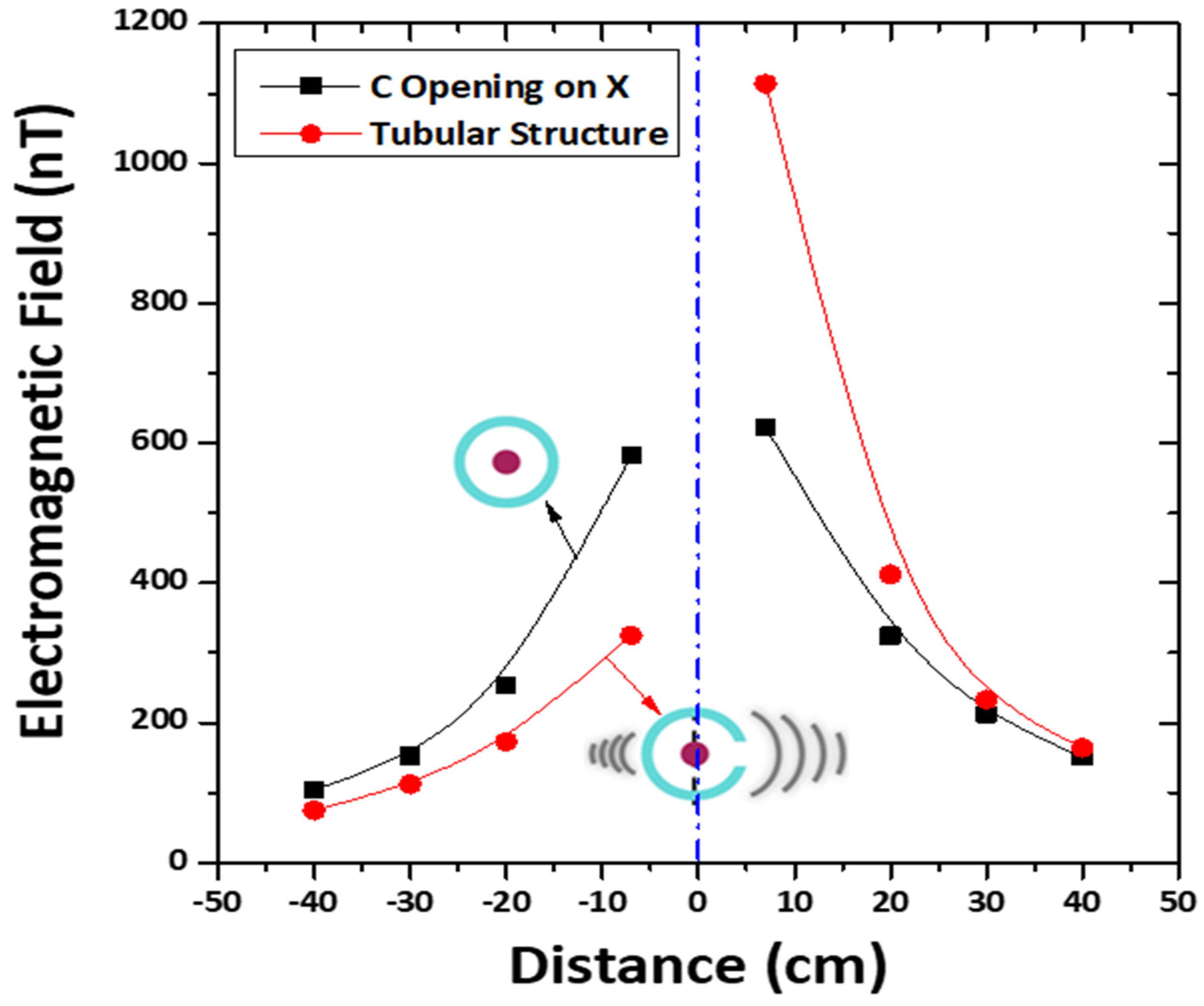
The effective results showed the degaussing rate of −5.06 dB when the electromagnetic field was shielded at the −7 cm position, and that of +5.05 dB when the enhanced electromagnetic field was shielded at the +7 cm position beyond experimental errors, as shown in Figure 5 and Table 3. In Figure 2 and Figure 5, it is worthy to mention the magnetic field distribution as a function of the distance was not symmetrical, because the single opening on the high-permeability material directed the emission of the ELF from line currents. The C-shaped permalloy tube did collect electromagnetic fields and emitted them from the opening space. As the electromagnetic field decayed rapidly with the distance, the reinforcement of permalloy was not obvious due to the low electromagnetic field as well. The C-shaped cylindrical device demonstrated here was only a one-dimensional device. It is easy to assemble C-shaped cylindrical devices in the three-dimensional space for more advanced applications.
4. Conclusions
This paper provides new C-shaped tube winding electrical coils with high-permeability passive shielding advantages for the direct conversion of magnetic fields. The results showed that it enhanced the electromagnetic field from +5.05 dB to +7 cm in the open direction and emitted −5.06 dB of electromagnetic noise at the same distance in the opposite direction. In conclusion, to reduce the same magnetic field, we can save 43.64% energy by using C-shaped permalloy materials. Furthermore, this study can mitigate the EMI effect on operators who are exposed to electromagnetic fields in another area when using active shielding.
This study laid a base to use C-shaped permalloy materials for mitigating the EMI problem. Meanwhile, this study demonstrated that EMF can be directive. In addition, how the C-shape’s opening size, opening angles, and radius affect the EMF could be further researched. Although the electric current in this study was low, it was presented that the C-shaped composite device is more convincing and the results with the C-shaped composite device will be better with a high current. The extremely low electromagnetic field not only greatly influences the semiconductor’s foundry in the examination process, but also the health monitoring in daily life. Therefore, C-shaped cylindrical devices can be modern indoor instruments to protect people from the exposure risk of electromagnetic waves.
Author Contributions
Conceptualization, Y.-L.S. and L.-M.C.; investigation, Y.-L.S. and L.-M.C.; methodology, Y.-L.S. and H.-Y.W.; validation, H.-Y.W. and L.-M.C.; writing—review and editing, L.-M.C. and Y.-L.S.; software, M.K.R. and H.-Y.W.; data curation, M.K.R. and H.-Y.W.; writing—original draft, M.K.R.; funding acquisition, L.-M.C. All authors have read and agreed to the published version of the manuscript.
Funding
This research was funded by the Ministry of Science and Technology, Taiwan, through grants MOST 109-2221-E-002-023-, MOST 110-2221-E-002-165-, and MOST 110-2622-E-468-002.
Institutional Review Board Statement
Not applicable.
Informed Consent Statement
Not applicable.
Data Availability Statement
The study did not report any data.
Acknowledgments
This work was supported in part by the Ministry of Science and Technology, Taiwan, through grants MOST 109-2221-E-002-023-, MOST 110-2221-E-002-165-, and MOST 110-2622-E-468-002.
Conflicts of Interest
The authors declare no conflict of interest.
References
- Gallastegi, M.; Jiménez-Zabala, A.; Santa-Marina, L.; Aurrekoetxea, J.J.; Ayerdi, M.; Ibarluzea, J.; Kromhout, H.; González, J.; Huss, A. Exposure to extremely low and intermediate-frequency magnetic and electric fields among children from the INMA-Gipuzkoa cohort. Environ. Res. 2017, 157, 190–197. [Google Scholar] [CrossRef] [PubMed]
- Aerts, S.; Calderon, C.; Valič, B.; Maslanyj, M.; Addison, D.; Mee, T.; Goiceanu, C.; Verloock, L.; Bossche, M.V.D.; Gajšek, P.; et al. Measurements of intermediate-frequency electric and magnetic fields in households. Environ. Res. 2017, 154, 160–170. [Google Scholar] [CrossRef] [PubMed] [Green Version]
- Shindo, D.; Akase, Z. Direct observation of electric and magnetic fields of functional materials. Mater. Sci. Eng. R Rep. 2020, 142, 100564. [Google Scholar] [CrossRef]
- Akase, Z.; Higo, M.; Shimada, K.; Sato, T.; Magara, H.; Shindo, D.; Ohno, N. Advanced Electron Microscopy for Materials Science. Mater. Trans. 2021, 62, 1589–1595. [Google Scholar] [CrossRef]
- Ji, W.; Huang, H.; Deng, A.; Pan, C. Effects of static magnetic fields on Escherichia coli. Micron 2009, 40, 894–898. [Google Scholar] [CrossRef] [PubMed]
- Semiconductor Industry Association. International Roadmap for Semiconductors (ITRS). 2007 edition. [2010-03-20]. 2009. Available online: http://public.itrs.net (accessed on 10 June 2021).
- Hoefflinger, B. ITRS: The international technology roadmap for semiconductors. In Chips 2020; Springer: Berlin/Heidelberg, Germany, 2011; pp. 161–174. [Google Scholar]
- Semiconductor Industry Association. International Technology Roadmap for Semiconductors. Available online: http://www.itrs.net (accessed on 9 August 2021).
- Rider, G.C. Current understanding of the electrostatic risk to reticles used in microelectronics and similar manufac-turing processes. J. Micro/Nanolithogr. MEMS MOEMS 2018, 17, 020901. [Google Scholar] [CrossRef] [Green Version]
- Verma, A. Possible Effects of Electromagnetic Fields (Emf) On Human Health. IJRAR-Int. J. Res. Anal. Rev. (IJRAR) 2021, 8, 917–920. [Google Scholar]
- Chan, G.; Mak, S.L.; Tsang, K.F.; Lee, C.C. Safety and EMC compliance with fabrication equipment in semicon-ductor industry: Challenges and solutions. In Proceedings of the 2019 IEEE Symposium on Product Compliance Engineering (SPCE Austin), Austin, TX, USA, 11–12 November 2019; pp. 1–6. [Google Scholar]
- Chuang, F.-C.; Song, Y.-L.; Yu, C.; Shsu, S.-G.; Ma, T.-G.; Wu, T.-L.; Chang, L.-M.; Yang, C.-Y. Active field canceling system in next generation nano-Fab. In Proceedings of the 4th International Conference on Power Electronics Systems and Applications, Hong Kong, China, 8–10 June 2011; pp. 1–4. [Google Scholar] [CrossRef]
- Mishra, R.K.; Thomas, M.G.; Abraham, J.; Joseph, K.; Thomas, S. Electromagnetic Interference Shielding Materials for Aerospace Application. Adv. Mater. Electromagn. Shielding Fundam. Prop. Appl. 2018, 327–365. [Google Scholar] [CrossRef]
- Pavelek, M.; Frivaldsky, M.; Spanik, P. Influence of the passive shielding on the optimal working point of the wireless power transfer systems. In Proceedings of the International Symposium on Power Electronics, Electrical Drives, Automation and Motion (SPEEDAM), Amalfi, Italy, 20–22 June 2018; pp. 773–778. [Google Scholar] [CrossRef]
- Jeschke, S.; Maarleveld, M.; Baerenfaenger, J.; Hirsch, H.; Tsiapenko, S.; Waldera, C.; Obholz, M. Development of a passive impedance network for modeling electric vehicle traction batteries for EMI measurements. In Proceedings of the 2017 International Symposium on Electromagnetic Compatibility-EMC EUROPE, Angers, France, 4–7 September 2017; pp. 1–6. [Google Scholar] [CrossRef]
- Canova, A.; Del-Pino-López, J.C.; Giaccone, L.; Manca, M. Active Shielding System for ELF Magnetic Fields. IEEE Trans. Magn. 2015, 51, 1–4. [Google Scholar] [CrossRef]
- Park, J.; Kim, D.; Hwang, K.; Park, H.H.; Kwak, S.I.; Kwon, J.H.; Ahn, S. A Resonant Reactive Shielding for Planar Wireless Power Transfer System in Smartphone Application. IEEE Trans. Electromagn. Compat. 2017, 59, 695–703. [Google Scholar] [CrossRef]
- Sim, B.; Lho, D.; Park, D.; Park, H.; Kang, H.; Kim, J. A Deep Neural Network-based Estimation of EMI Reduction by an Intermediate Coil in Automotive Wireless Power Transfer System. In Proceedings of the 2020 IEEE International Symposium on Electromagnetic Compatibility & Signal/Power Integrity (EMCSI), Reno, NV, USA, 28 July–28 August 2020; pp. 407–410. [Google Scholar] [CrossRef]
- Azadian, S.; Tehranchi, M.; Mohseni, S.M.; Mohseni, S.M. Reduction and control of permalloy thin film damping factor under microwave irradiation. J. Alloys Compd. 2017, 723, 960–966. [Google Scholar] [CrossRef]
- Zhi, C.; Shinshi, T.; Saito, M.; Kato, K. Planar-type micro-electromagnetic actuators using patterned thin film permanent magnets and mesh type coils. Sens. Actuators Phys. 2014, 220, 365–372. [Google Scholar] [CrossRef]
- Cruz, P.; Izquierdo, C.; Burgos, M. Optimum passive shields for mitigation of power lines magnetic field. IEEE Trans. Power Deliv. 2003, 18, 1357–1362. [Google Scholar] [CrossRef]
- Roccella, M.; Lucca, F.; Roccella, R.; Pizzuto, A.; Ramogida, G.; Portone, A.; Tanga, A.; Formisano, A.; Martone, R. Analysis of active and passive magnetic field reduction systems (MFRS) of the ITER NBI. Fusion Eng. Des. 2007, 82, 709–715. [Google Scholar] [CrossRef]
- Qader, M.A.; Vishina, A.; Yu, L.; Garcia, C.; Singh, R.; Rizzo, N.; Huang, M.; Chamberlin, R.; Belashchenko, K.; van Schilfgaarde, M.; et al. The magnetic, electrical and structural properties of copper-permalloy alloys. J. Magn. Magn. Mater. 2017, 442, 45–52. [Google Scholar] [CrossRef] [Green Version]
- Trzynadlowski, A.M. EMI Effects of Power Converters, 3rd ed.; Elsevier: Amsterdam, The Netherlands, 2011; pp. 1229–1245. [Google Scholar] [CrossRef]
- Schulz, R.B.; Plantz, V.C.; Brush, D.R. Shielding theory and practice. IEEE Trans. Electromagn. Compat. 1988, 30, 187–201. [Google Scholar] [CrossRef]
- Saito, T. Shielding Performance of Open-Type Magnetic Shielding Box Structure. IEEE Trans. Magn. 2009, 45, 4640–4643. [Google Scholar] [CrossRef]
- Oschman, J.L. Chapter 16—The Electromagnetic Environment, 2nd ed.; Elsevier: Amsterdam, The Netherlands, 2016; pp. 269–295. [Google Scholar] [CrossRef]
- Wen, H.-Y. Dissertation: High-Tech Plant Environmental Quality—Study on Electromagnetic Wave; Department of Civil Engineering College of Engineering, National Taiwan University: Taipei, Taiwan, 2013. [Google Scholar]
- Chang, L.-M.; Song, Y.-L. Magnetic Field Zooming Structure for Wire. Patent TWM475682U, 2014. [Google Scholar]
- Pratap, V.; Soni, A.; Dayal, S.; Abbas, S.; Siddiqui, A.; Prasad, N. Electromagnetic and absorption properties of U-type barium hexaferrite-epoxy composites. J. Magn. Magn. Mater. 2018, 465, 540–545. [Google Scholar] [CrossRef]
- Choubani, F.; Dávid, J.; Mastorakis, N. Experiment on the Shielding by Hollow Conducting Tubes. IEEE Trans. Electromagn. Compat. 2006, 48, 342–347. [Google Scholar] [CrossRef]
Figure 1.
Measurement of the electromagnetic field in the C-shape high-permeability material. (a) Instrument setup. The C-opening in the vertical (i.e., the Y-axis) direction (b) and horizontal (i.e., the X-axis) direction (c). The line currents ran in the coil as indicated by the Z-axis.
Figure 1.
Measurement of the electromagnetic field in the C-shape high-permeability material. (a) Instrument setup. The C-opening in the vertical (i.e., the Y-axis) direction (b) and horizontal (i.e., the X-axis) direction (c). The line currents ran in the coil as indicated by the Z-axis.

Figure 2.
Electromagnetic field intensities emitted from the tubular structure without an opening (a) and the C-shape cylindrical device (b) by MagNet. (c) Electromagnetic field as a function of the distance.
Figure 2.
Electromagnetic field intensities emitted from the tubular structure without an opening (a) and the C-shape cylindrical device (b) by MagNet. (c) Electromagnetic field as a function of the distance.

Figure 3.
Setups with a C-shaped opening along the X-axis and Y-axis separately.

Figure 4.
The measured electromagnetic fields of the high-permeability material.

Figure 5.
The measured electromagnetic fields in the C-shape composite device.


Table 1.
Simulation data of electromagnetic fields.
| Distance (D; cm) | Electromagnetic Field (nT) | Efficiency (dB) | |
|---|---|---|---|
| Tubular Structure (T) | C-shape Composite Device (C) | ||
| −100 | 186 | 170 | −0.78 |
| −90 | 188 | 172 | −0.77 |
| −80 | 199 | 181 | −0.82 |
| −70 | 217 | 196 | −0.88 |
| −60 | 245 | 221 | −0.90 |
| −50 | 288 | 256 | −1.02 |
| −40 | 358 | 311 | −1.22 |
| −30 | 471 | 397 | −1.48 |
| −20 | 697 | 551 | −2.04 |
| −10 | 1424 | 855 | −4.43 |
| 10 | 1483 | 2022 | 2.69 |
| 20 | 701 | 879 | 1.97 |
| 30 | 473 | 557 | 1.42 |
| 40 | 357 | 405 | 1.10 |
| 50 | 287 | 322 | 1.00 |
| 60 | 245 | 271 | 0.88 |
| 70 | 216 | 238 | 0.84 |
| 80 | 199 | 217 | 0.75 |
| 90 | 189 | 206 | 0.75 |
| 100 | 185 | 202 | 0.76 |
Table 2.
Results of electromagnetic fields (peak value) in the C-shaped high-permeability material.
| Voltage (V) | Current (A) | Tubular Structure (T) in nT | C Opening (C) in nT | Efficiency (dB) | ||
|---|---|---|---|---|---|---|
| In the X-axis | In the Y-axis | In the X-axis | In the Y-axis | |||
| 2.5 | 0.39 | 904 | 805 | 842 | −1.01 | −0.62 |
| 2.0 | 0.31 | 730 | 640 | 670 | −1.14 | −0.74 |
| 1.5 | 0.22 | 526 | 430 | 501 | −1.75 | −0.42 |
| 1.0 | 0.15 | 379 | 337 | 353 | −1.02 | −0.62 |
| 0.5 | 0.07 | 194 | 171 | 179 | −1.10 | −0.70 |
Table 3.
Results of electromagnetic fields (peak value) in the C-shaped cylindrical device.
| Distance (D) in cm | Tubular Permalloy (T) in nT | C-shape Opening in the X-axis (C) in nT | Efficiency (dB) |
|---|---|---|---|
| 40 | 151 | 164 | 0.72 |
| 30 | 212 | 233 | 0.82 |
| 20 | 324 | 412 | 2.09 |
| 7 | 623 | 1114 | 5.05 |
| −7 | 582 | 325 | −5.06 |
| −20 | 253 | 173 | −3.30 |
| −30 | 153 | 112 | −2.71 |
| −40 | 104 | 75 | −2.84 |
Publisher’s Note: MDPI stays neutral with regard to jurisdictional claims in published maps and institutional affiliations. |
© 2022 by the authors. Licensee MDPI, Basel, Switzerland. This article is an open access article distributed under the terms and conditions of the Creative Commons Attribution (CC BY) license (https://creativecommons.org/licenses/by/4.0/).
Share and Cite
MDPI and ACS Style
Song, Y.-L.; Reddy, M.K.; Wen, H.-Y.; Chang, L.-M. Mitigation of Electro Magnetic Interference by Using C-Shaped Composite Cylindrical Device. Appl. Sci. 2022, 12, 882. https://0-doi-org.brum.beds.ac.uk/10.3390/app12020882
AMA Style
Song Y-L, Reddy MK, Wen H-Y, Chang L-M. Mitigation of Electro Magnetic Interference by Using C-Shaped Composite Cylindrical Device. Applied Sciences. 2022; 12(2):882. https://0-doi-org.brum.beds.ac.uk/10.3390/app12020882
Chicago/Turabian StyleSong, Yu-Lin, Manoj Kumar Reddy, Hung-Yung Wen, and Luh-Maan Chang. 2022. "Mitigation of Electro Magnetic Interference by Using C-Shaped Composite Cylindrical Device" Applied Sciences 12, no. 2: 882. https://0-doi-org.brum.beds.ac.uk/10.3390/app12020882
Note that from the first issue of 2016, this journal uses article numbers instead of page numbers. See further details here.