
Pulsed Laser Ablation: A Facile and Low-Temperature Fabrication of Highly Oriented n-Type Zinc Oxide Thin Films


1
Research Center on Advanced Materials and Technologies, Department of Exact and Natural Science, Institute of Interdisciplinary Research, Alexandru Ioan Cuza University of Iasi, Blvd. Carol I, no. 11, 700506 Iasi, Romania
2
Science Department & Research Institute for Agriculture and Environment, Iasi University of Life Sciences, 3 Sadoveanu Alley, 700490 Iasi, Romania
*
Authors to whom correspondence should be addressed.
†
These authors contributed equally to this work.
Appl. Sci. 2022, 12(2), 917; https://0-doi-org.brum.beds.ac.uk/10.3390/app12020917
Submission received: 5 December 2021
/
Revised: 12 January 2022
/
Accepted: 14 January 2022
/
Published: 17 January 2022
(This article belongs to the Special Issue Recent Advances in Application of Coatings and Films)
Abstract
:Eco-friendly and facile zinc oxide (ZnO) synthesis of zinc-oxide-based nanomaterials with specific properties is a great challenge due to its excellent industrial applications in the field of semiconductors and solar cells. In this paper, we report the production of zinc oxide thin films at relatively low deposition temperature employing a simple and non-toxic method at low substrate temperature: pulsed laser ablation, as a first step for developing a n-ZnO/p-Si heterojunction. Single-phase n-type zinc oxide thin films are confirmed by an X-ray diffraction (XRD) pattern revealed by the maximum diffraction intensity from the (002) plane. Absorbance measurements indicate an increase in the band gap energy close to the bulk ZnO. A 350 °C substrate temperature led to obtaining a highly porous film with high crystallinity and high bandgap, showing good premises for further applications.
1. Introduction
Over the past decades, the advancement in the field of thin films technology paved the road for development of various semiconductor-based devices [1,2,3]. In this context, zinc oxide (ZnO) thin films and nanostructures attracted a great interest, owing to their unique properties such as large exciton binding energy (60 meV), direct wide-bang gap of about 3.37 eV at room temperature, high optical transparency in the visible region, low electrical resistivity, as well as high electrochemical stability, high electron mobility, non-toxicity, and abundance in nature, therefore being used in a wide range of application in the UV region of optoelectronic devices [1,2,3,4,5,6,7,8,9,10,11,12,13].
Moreover, ZnO-based nanomaterials can be considered as promising candidates for solar cells, gas sensors, laser diodes, and so on. ZnO films can be grown by several physical and chemical methods such as sputtering, chemical vapor deposition, sol–gel method, molecular beam epitaxy, and pulsed laser deposition on a wide range of substrates [14,15,16,17,18]. Taking into consideration all these approaches, in the present context of using green technologies, not all techniques are considered clean, especially wet-chemical methods for which the chemical residues involved proved to be harmful. Thus, new approaches should be considered and refined. Laser ablation has been a well-studied techniques since its early days and it has been showing the premises to be implemented for the production of n-type ZnO thin films.
Pulsed laser deposition (PLD) has been studied and employed as a relatively simple and reliable technique for depositing a wide range of materials for novel applications [18,19,20,21,22,23]. Due to its versatility, flexibility, and process speed, the technique has emerged as a suitable production method for almost any material, ranging from simple materials (metals, oxides, semiconductors) to complex multilayer and multicomponent compounds and even biological materials with stoichiometric transfer of materials from the target [17,18,19,20,21]. Being a physical vapor deposition process that can be carried out in high vacuum, atmosphere, and even in liquids, the technique has attracted high interest in many fields. Among other advantages, the PLD technique offers the possibility of producing good quality transparent films [22,23].
Excimer lasers represent one of the most popular gas-based lasers, generating intense short pulses in the ultraviolet spectrum. During the last decades, they have undergone rapid technological advancement, becoming one of the most utilized tools for the deposition of thin film nanomaterials. One of the biggest advantages of excimer lasers is represented by the very high gain excimer medium that can provide an adequate output for various applications that cover a broad range of applications from research to medical and even industrial ones. Excimer lasers have the ability to produce a wide range of processing power with variable repetition rates. The most often used emission lines of excimer lasers are 193 nm (ArF) and 248 nm (KrF) due to the ability of reaching high pulse energies (hundreds of mJ and even more) with high frequencies (1–50 Hz). Shot-to-shot stability is critical in PLD because it facilitates the reproducibility and stoichiometry of the thin film materials. Ceramic pre-ionization technology, part of the excimer laser, provides superior pulse-to-pulse stability at high pulse energy and adjustable repletion rates. For PLD, a high pulse energy laser fluence is imperative to vaporize any bulk material, making excimer lasers suitable for the high-precision deposition of nanostructured materials.
It is well established that pure undoped ZnO films generally indicate n-type conduction. Silicon is a suitable material for integration in optoelectronic devices due to its low cost. Our final aim is to create a heterojunction of n-ZnO/p-Si that has the potential of being integrated in a wide range of applications such as gas sensors, solar cells, photodiodes, and many others [24,25,26,27]. As an initial step towards our goal, in this study we focus on the preparation of highly oriented ZnO thin films by pulsed laser deposition at relatively low substrate temperatures. We take advantage of the PLD technique, namely, by the possibility of controlling the elemental composition of the deposited thin films much better than using other methods. The structure, morphology, composition, and optical properties of the obtained films are characterized by means of X-ray diffraction (XRD), scanning electron microscopy (SEM), and energy-dispersive X-ray spectroscopy (EDS) UV-VIS measurements.
2. Materials and Methods
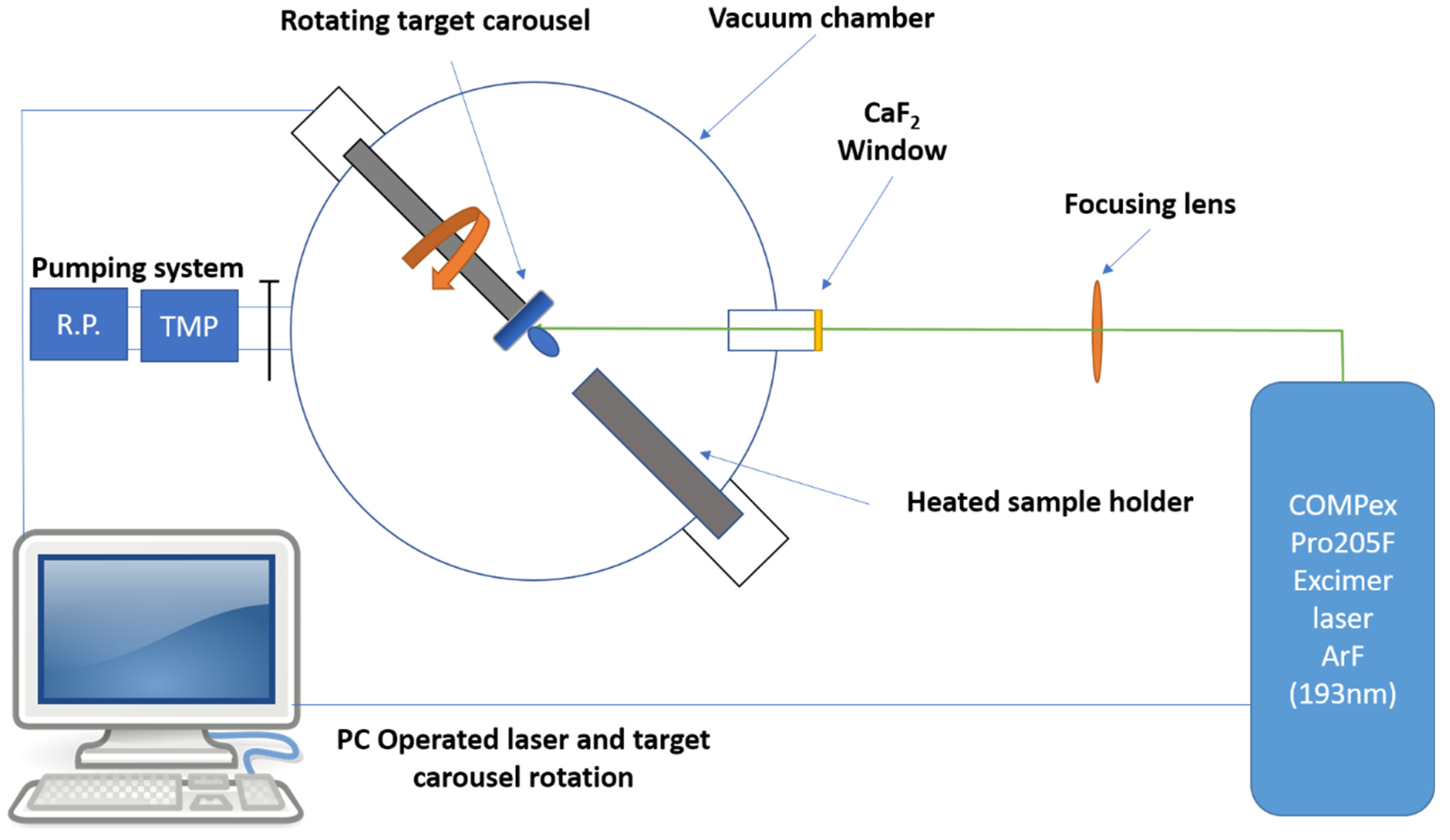
The ZnO thin films were deposited on commercially available silicon wafers (cut 5 × 5 mm) using an ArF laser with a wavelength of 193 nm (Coherent COMPex Pro 205F) by ablating a sintered ZnO target in high purity (99.999%) oxygen atmosphere. ZnO target was sintered from ZnO high purity powder (Sigma Aldrich) and baked for 12 h at a temperature of 1100 °C. The laser repetition rate can be varied from 1 to 50 Hz, and the energy per pulse can be set in the range of 10 to 400 mJ. For this study, the laser was operated at a frequency of 10 Hz with a constant power of 300 mJ. The experimental apparatus consists of a vacuum chamber that can be evacuated to a base pressure of 4 × 10⁻⁷ mbarr with the help of a rotary pump coupled with a turbomolecular one as seen in Figure 1. Before being loaded in the chamber and mounted on the sample holder, the substrates were ultrasonically cleaned with ethanol for at least 30 min and dried in air.
The temperature of the substrate during deposition can be varied from room temperature to a maximum of 800 °C. To remove the contaminants from the surface of the target, before each deposition, the target is cleaned by ablation operating the laser for 5000 pulses. Inside the vacuum chamber, the targets can be mounted on a carousel that can accommodate a maximum number of 6 different targets and that can be operated automatically for multi-layer deposition of various materials. During operation, the target is rotated and has a translational movement as well to maintain the uniformity of the target surface and also the stoichiometry of the deposited thin films. In this study, for each condition, multiple batches of samples were prepared. Since the plasma plume volume is limited, for the uniformity of the films and reproducibility of the experiments, only four substrates are mounted at a time on the heated sample holder. The surface of the target is repolished after each deposition to keep it flat. In all cases, the distance between target and substrate was kept constant at 5 cm. The schematic diagram of the experimental setup is depicted in Figure 1. In all conditions, the deposition took place at 50,000 pulses, thus, despite changing the substrate temperature in the mentioned range, the deposition rate is similar for all studied cases.
The crystallographic structure of the deposited thin films was characterized by X-ray diffraction (XRD) using a Shimadzu LabX XRD 6000 Diffractometer system with a CuKα (λ = 1.5406 Å) source. The surface morphology was investigated using scanning electron microscopy (SEM) (Quanta 450, FEI, Thermo Fisher Scientific, Hillsboro, OR, USA). The samples were analyzed as they were, the system being able to image conductive and non-conductive samples as well without any prior preparation. The elemental composition analysis was performed with an energy dispersive X-ray spectrometry (EDS) module coupled with an SEM machine (EDAX, Ametek Inc., Berwyn, PA, USA). Absorbance measurements were obtained with a UV-VIS spectrophotometer (Thermo Scientific Evolution 300, Thermo Fisher Scientific, Hillsboro, OR, USA). Each of the above-mentioned measurements were performed on at least three of the samples for each experiment.
3. Results and Discussions
3.1. Structural Properties
The crystalline phase and orientation of the ZnO thin films was determined by XRD measurements using Scherrer’s formula [28] to calculate the crystalline size:
where the constant k = 0.94 is the shape factor, λ is the wavelength of X-rays 1.5406 Å for Cu Kα, θ is the Bragg’s angle, and β is the full width at half maximum.
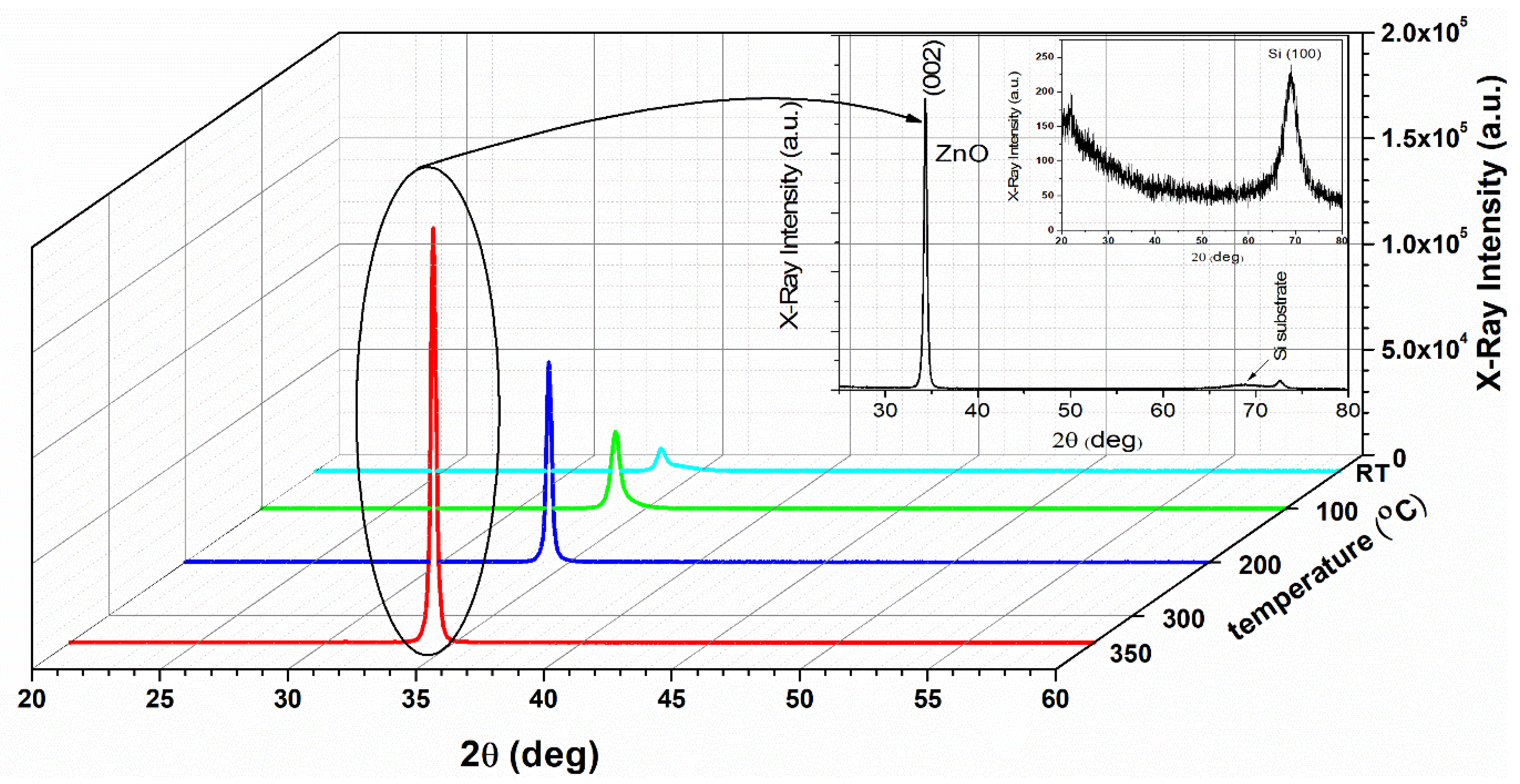
From the diffraction patterns, a good crystalline behavior is revealed with a preferential growth of the thin films on the (002) plane, suggesting that there are no secondary phases, as seen from Figure 2. The inset of the figure depicts the crystalline phase and orientation of the Si substrate as measured by XRD. The position of the (002) is consistent with the values from literature: PDF card no 00-005-0664.
Knowing the structure of the (002) diffraction peaks, the crystalline plane distance d, the lattice constant c, and the strain ε of the ZnO thin films are calculated. The crystalline distance d for the index (002) is given by the Bragg formula:
and the lattice constant c is equal to 2 d [28]. The strain ε in the films along the c-axis is calculated by the formula:
where c0 is the unstrained lattice constant and has a value of 0.5205 nm for bulk ZnO [29]. The calculated values are presented in Table 1. The positive value for the strain ε depicts a very low tensile strain of ZnO thin films approaching an almost stress-free ZnO. The intensity of the (002) diffraction peak increases as a function of substrate temperature and is revealing an improvement of the film’s crystallinity. The film deposited at room temperature exhibits a lower crystallinity compared with those deposited at about 350 °C. The annealing of different layers induced changes in the crystalline lattice constant of ZnO, which changed the tensile stress in the ZnO thin films. A shift toward a high angle of the XRD peak is observed due to the narrowing of the distance d between the lattice planes. As a result, preferentially c-plane-oriented, highly crystalline ZnO thin films are produced.
d = λ/2 sinθ
ε = (c − c0)/c0
3.2. Surface Morphology and Chemical Composition
To distinguish between n-type and p-type conductivity of the deposited ZnO thin films, a simple method developed by Benedict Wen-Cheun Au et al. was employed [30]. Hot-point probe measurements have been successfully utilized to determine the conductivity type of materials as an alternative for the time-consuming Hall-effect measurements. Using simple laboratory equipment, mainly a soldering iron station, a multimeter, and a pair of probes, it is possible to measure the nature of the thin films and the conductivity of the films by evaluating whether the voltage between hot and cold probes is positive or negative. The n-type nature of the ZnO is usually given by the point’s defects present in its lattice [31]. The hot probe is obtained by heating up the positive probe that thermally excites the carries, electrons in the case of n-type ZnO, that diffuse from a high carrier concentration region to a low carrier concentration region in all directions. When a positive voltage is generated between a hot and cold probe, the thin films are of n-type conduction. The method is employed only to depict the fact that the thin ZnO films exhibits n-type conductivity and does not give absolute values.
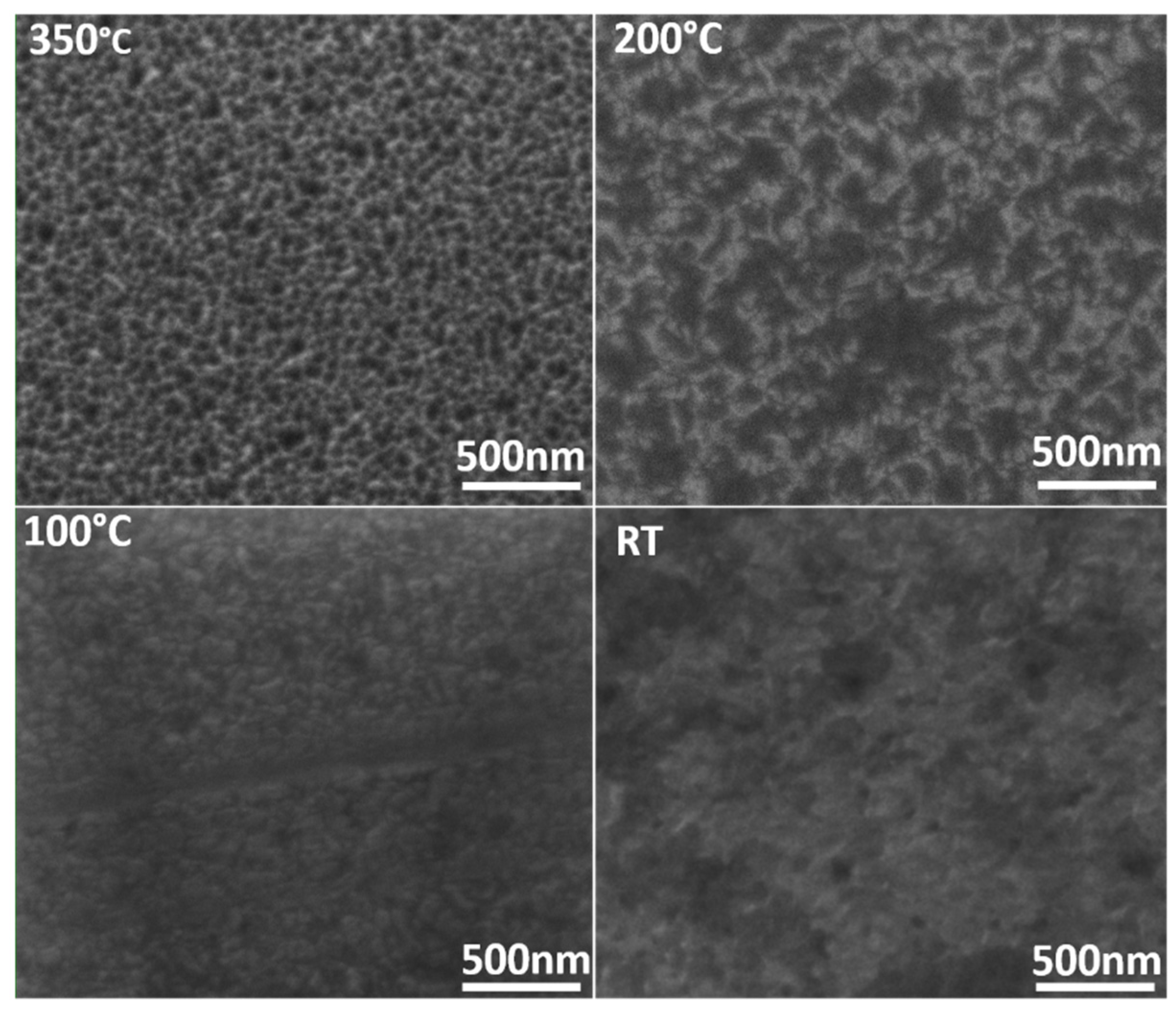
Figure 3 shows the surface of the thin films obtained for different substrate temperatures. It is clearly seen that this is a crucial factor that dictates the morphology, as found for other deposition methods as well such as sputtering—the ratio between the temperature of the substrate and the melting temperature of the deposited material influences the porosity of the deposited films [32]. The porosity of the films is important in applications such as the fabrication of dye-synthesized solar cells and lithium cells but also in designing p-type doped ZnO structures [33]. The obtained films seem to have a wall-like structure for 200 and 350 °C, due to the substrate temperature that dictates the nucleation process, and determines a two-dimensional growth. At low temperature, it was shown that the atoms remain in the place where they land without too much diffusion in the surface, the process being considered as a quench growth. Figure 3 shows that for room temperature and 100 °C, the substrates seem to be covered by clusters of nanoparticles that develop in a dense film [17,34]. It seems that, starting from a specific temperature, the porous structure would be initially composed of small grains that would promote the growth of fine particles, limiting the preferential growth along specific directions and affecting the crystallinity of the thin films. For temperatures higher than 350 °C, we found that the films have a more grain-like structure, with large exposure of the substrate that makes them unsuitable for the applications we envisioned. This fact corresponds with other reports and was the reason why we have chosen the studied temperatures [25,35,36].
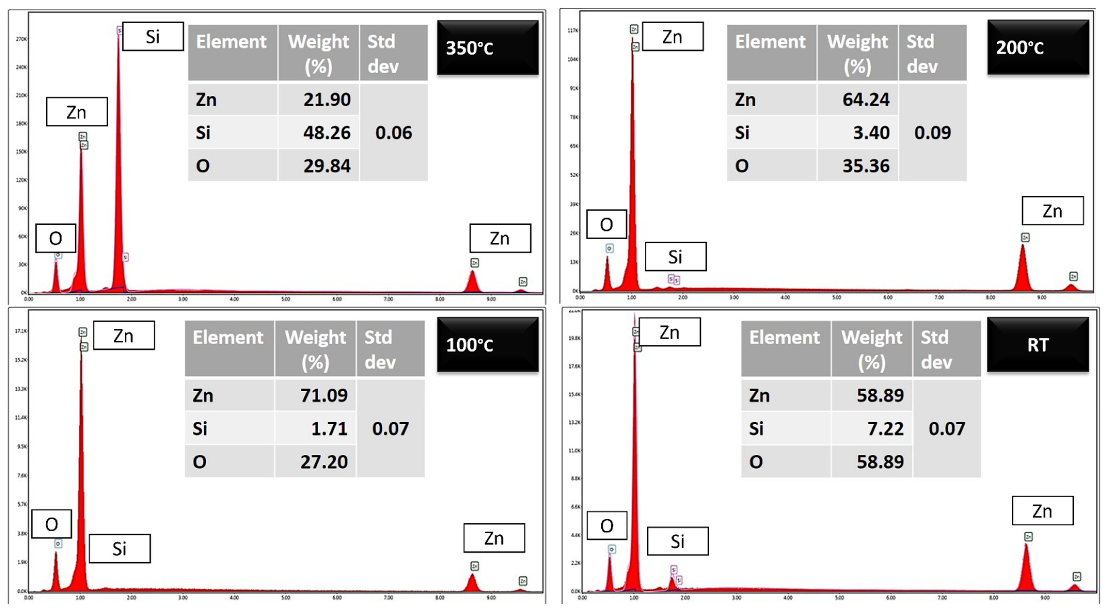
EDS spectra of the ZnO thin films are presented in Figure 4. For each of the samples, Zn and O are the main constituents, with no trace of impurities (within the detection limit of EDS) with respect to substrate temperature used during PLD deposition. For the samples deposited at 350 °C, the EDS spectrum also shows an increase in the Si signal related with the substrate. In this case, as seen from the SEM micrographs of the deposited material, the substrate detection indicates an increase in the porosity, thus, the electron beam not only reaches the film but also the substrate through the formed pores. In the studied conditions, all the films have approximately the same thickness, the deposition rate being similar. Therefore the increase in the Si peak can only be related to the exposure of the substrate through the porosity of the film. Relative values of the measured elements can be obtained from the EDS measurements. Before the analysis, the device is semi-automatically calibrated using a standard AlCu sample; the operating software collects a spectrum checking the relative intensity of Al Kα and Cu Kα peaks and their corresponding energies and makes adjustments for different amplification times for fine calibration using an automatic procedure. From the spectra presented in Figure 4, a quantification of the elements or oxide ratios can be performed automatically by the software (TEAMS ver. 4.1, EDAX Inc., Mahwah, NJ, USA). For the studied conditions, the average relative elemental concentrations estimated from the spectra are also shown in Figure 4.
3.3. Optical Characterization
The optical absorption of the ZnO thin films was measured at room temperature using a UV-visible spectrophotometer within the range of 300 to 1100 nm. In Figure 5, the absorption spectra for ZnO thin films deposited at substrate temperatures of 350 °C, 200 °C, 100 °C, and room temperature are presented. All the films exhibited a sharp absorption edge in the UV region at about 390 nm. Using the absorbance data, the direct transition band gap energies (Eg) were calculated based on Tauc’s equation [37]:
where α is the absorption coefficient, A is the band edge sharpness constant, Eg is the band gap, and hν is the incident photon energy. By plotting (αhν)2 versus the incident photon energy, the Tauc’s plots are obtained, all the data being presented in Figure 5. By regressing to zero the linear portion of the (αhν)2 from Tauc plot, the energy band gap of the thin films is found. The values obtained were as follows: 3.32 eV, 3.25 eV, 3.13 eV, and 3.12 eV for the films deposited at 350 °C, 200 °C, 100 °C, and room temperature, respectively. Compared to the value of 3.37 eV for bulk ZnO, the obtained values of the energy gap are slightly smaller for the films deposited at temperatures lower than 300 °C as a consequence of various defects and zinc and/or oxygen vacancies present in the lattice of ZnO. As for the higher deposition temperature, it is clearly seen that the energy band gap is approaching the ideal value for bulk ZnO (~3.7 eV) [1]. This conclusion supports the improvement of the crystallinity of the thin films as seen from the XRD measurements earlier discussed.
4. Conclusions
Preferentially c-plane-oriented, highly crystalline ZnO thin films were obtained using pulsed laser deposition of a ZnO target in oxygen atmosphere as a first step in the development of an n-ZnO/p-Si heterojunction for applications. The dependence of the thin films structure and properties was observed as a function of the substrate temperature. The crystallinity increased for the thin films with the increasing temperature from room temperature to 350 °C. The same behavior was observed for the band gap that changed from 3.12 eV at room temperature, close to the ideal value for the highest substrate temperature studied, with a value of 3.32 eV. The 350 °C substrate temperature indicated a different crystallization process as compared to lower temperatures, resulting in a highly porous film with high crystallinity and high bandgap, showing good premises for using PLD in the above-mentioned conditions to produce n-type ZnO thin films with the desired properties.
Author Contributions
M.A.C.: conceptualization, methodology, validation, formal analysis, investigation, data curation, writing—original draft preparation; I.M.: formal analysis, data curation, investigation, writing—review and editing. All authors have read and agreed to the published version of the manuscript.
Funding
This work was supported by a grant by “Alexandru Ioan Cuza” University of Iasi, within the research Grants program, Grant UAIC no. GI-UAIC-2020-05.
Institutional Review Board Statement
Not applicable.
Informed Consent Statement
Not applicable.
Acknowledgments
The authors would like to thank Dr. Georgiana Bulai (https://ici.uaic.ro/en/scientific-researcher-iii-andreea-georgiana-bulai/) from Integrated Center of Environmental Science Studies in the North-Eastern Development Region (CERNESIM), Department of Exact and Natural Sciences, Institute of Interdisciplinary Research, Alexandru Ioan Cuza University of Iasi, for assisting with the XRD measurements, and Dr. Ionut Topala (https://www.plasma.uaic.ro/index.php/staff/ionut-topala/) from Alexandru Ioan Cuza University of Iasi, Faculty of Physics, Iasi Plasma Advanced Research Center (IPARC), for assisting with the UV-VIS measurements.
Conflicts of Interest
The authors declare no conflict of interest.
References
- Thomas, D.G. The exciton spectrum of zinc oxide. J. Phys. Chem. Solids 1960, 15, 86–96. [Google Scholar] [CrossRef]
- Burgess, R. Semiconductor Physics. Nature 1957, 180, 1265–1266. [Google Scholar] [CrossRef]
- Di Mauro, A.; Fragala, M.E.; Privitera, V.; Impellizzeri, G. ZnO for application in photocatalysis: From thin films to nanostructures. Mat. Sci. Semicond. Process. 2017, 69, 44–51. [Google Scholar] [CrossRef]
- Laurenti, M.; Cauda, V. Porous Zinc Oxide Thin Films: Synthesis Approaches and Applications. Coatings 2018, 8, 67. [Google Scholar] [CrossRef] [Green Version]
- Bunn, C.W. The lattice-dimensions of zinc oxide. Proc. Phys. Soc. Lond. 1935, 47, 835. [Google Scholar] [CrossRef]
- Heller, R.B.; McGannon, J.; Weber, A.H. Precision Determination of the Lattice Constants of Zinc Oxide. J. Appl. Phys. 1950, 21, 1283. [Google Scholar] [CrossRef]
- Moezzi, A.; McDonagh, A.M.; Cortie, M.B. Zinc oxide particles: Synthesis, properties and applications. Chem. Eng. J. 2012, 185–186, 1–22. [Google Scholar] [CrossRef]
- Chu, S.; Olmedo, M.; Yang, Z.; Kong, J.; Liu, J. Electrically pumped ultraviolet ZnO diode lasers on Si. Appl. Phys. Lett. 2008, 93, 181106. [Google Scholar] [CrossRef] [Green Version]
- Dietl, T.; Ohno, H.; Matsukura, F.; Cibert, J.; Ferrand, D. Zener Model Description of Ferromagnetism in Zinc-Blende Magnetic Semiconductors. Science 2000, 287, 1019. [Google Scholar] [CrossRef] [Green Version]
- Wang, H.T.; Kang, B.S.; Ren, F.; Tien, L.C.; Sadik, P.W.; Norton, D.P.; Pearton, S.J.; Lin, J. Hydrogen-selective sensing at room temperature with ZnO nanorods. Appl. Phys. Lett. 2005, 86, 243503. [Google Scholar] [CrossRef]
- Look, D.C. Recent advances in ZnO materials and devices. Mater. Sci. Eng. B 2001, 80, 383–387. [Google Scholar] [CrossRef]
- Jiang, Z.; Soltanian, S.; Gholamkhass, B.; Aljaafari, A.; Servati, P. Light-soaking free organic photovoltaic devices with sol–gel deposited ZnO and AZO electron transport layers. RSC Adv. 2018, 8, 36542–36548. [Google Scholar] [CrossRef] [Green Version]
- Han, J.; Fan, F.; Xu, C.; Lin, S.; Wei, M.; Duan, X.; Wang, Z.L. ZnO nanotube-based dye-sensitized solar cell and its application in self-powered devices. Nanotechnology 2010, 21, 405203. [Google Scholar] [CrossRef] [PubMed]
- Winantyo, R.; Murakami, K. ZnO Nanorods Formation for Dye-Sensitized Solar Cells Applications. Int. J. Technol. 2017, 8, 1462–1469. [Google Scholar] [CrossRef] [Green Version]
- Morales, C.; Leinen, D.; del Campo, A.; Ares, J.R.; Sanchez, C.; Flege, J.I.; Gutierrez, A.; Preito, P.; Soriano, L. Growth and characterization of ZnO thin films at low temperatures: From room temperature to −120 °C. J. Alloys Compd. 2021, 884, 161056. [Google Scholar] [CrossRef]
- Habibi, A.; Vatandoust, L.; Aref, S.M.; Naghshara, H. Formation of high performance nanostructured ZnO thin films as a function of annealing temperature: Structural and optical properties. Surf. Interfaces 2020, 21, 100723. [Google Scholar] [CrossRef]
- Ogugua, S.N.; Ntwaeaborwa, O.M.; Swart, H.C. Latest development on pulsed laser deposited thin films for advanced luminescence applications. Coatings 2020, 10, 1078. [Google Scholar] [CrossRef]
- Simdar, M.; Mousavi, S.S.; Sajad, B.; Hassani, F. Distinctive ZnO film’s structures and morphologies for different modes of heating substrate. Mater. Lett. 2021, 297, 129914. [Google Scholar] [CrossRef]
- Christen, H.M.; Eres, G. Recent advances in pulsed-lased deposition of complex oxides. J. Phys. Condens. Matter. 2008, 20, 264005. [Google Scholar] [CrossRef] [Green Version]
- Caricato, A.P.; Luches, A. Applications of the matrix-assisted pulsed laser evaporation method for the deposition of organic, biological and nanoparticle thin films: A review. Appl. Phys. A 2011, 105, 565–582. [Google Scholar] [CrossRef]
- Yao, J.D.; Zheng, Z.Q.; Wang, G.W. Production of large-area 2D materials for high-performance photodetectors by pulsed-laser deposition. Prog. Mater. Sci. 2019, 106, 100573. [Google Scholar] [CrossRef]
- Franklin, J.B.; Zou, B.; Petrov, P.; McComb, D.W.; Ryan, M.P.; McLachlan, M.A. Optimized pulsed laser deposition of ZnO thin films on transparent conducting substrates. J. Mater. Chem. 2011, 21, 8178–8182. [Google Scholar] [CrossRef]
- Socol, G.; Socol, M.; Stefan, N.; Axente, E.; Popescu-Pelin, G.; Craciun, D.; Duta, L.; Mihailescu, C.M.; Mihailescu, I.N.; Stanculescu, A.; et al. Pulsed laser deposition of transparent conductive oxide thin films on flexible substrates. Appl. Surf. Sci. 2012, 260, 42–46. [Google Scholar] [CrossRef]
- Fan, J.C.; Streekanth, K.M.; Xie, Z.; Chang, S.L.; Rao, K.V. p-type ZnO materials, theory, growth, properties and devices. Prog. Mater. Sci. 2013, 58, 874–985. [Google Scholar] [CrossRef]
- Das, D.; Karmakar, L. Optimization of Si doping in ZnO thin films and fabrication of n-ZnO:Si/p-Si heterojunction solar cells. J. Alloys Compd. 2020, 824, 153902. [Google Scholar] [CrossRef]
- Nguyen, V.H.; Resende, J.; Jimenez, C.; Deschanvres, J.L.; Carroy, P.; Munoz, D.; Bellet, D.; Munoz-Rojas, D. Deposition of ZnO based thin films by atmospheric pressure spatial atomic layer deposition for application in solar cells. J. Renew. Sustain. Energy 2017, 9, 021203. [Google Scholar] [CrossRef]
- Rasool, A.; Santhosh Kumar, M.C.; Mamat, M.H.; Gopalakrishnan, C.; Amiruddin, R. Analysis on different detection mechanisms involved in ZnO-based phtotodetector and photodiodes. J. Mater. Sci. Mater. Electron. 2020, 31, 7100–7113. [Google Scholar] [CrossRef]
- Cullity, B.D. The Elements of X-Ray Diffraction; Addison-Wesley Publishing Company Inc.: Reading, MA, USA, 1978; p. 102. [Google Scholar]
- Ahn, C.H.; Kim, Y.Y.; Kim, D.C.; Mohanta, S.K.; Cho, H.K. A comparative analysis of deep level emission in ZnO layers deposited by various methods. J. Appl. Phys. 2009, 105, 089902. [Google Scholar] [CrossRef] [Green Version]
- Wen-Cheun Au, B.; Chan, K.-Y.; Sin, Y.-K.; Ng, Z.-N. Hot-point probe measurements of N-type and P-type ZnO films. Microelectron. Int. 2017, 34, 30–34. [Google Scholar] [CrossRef]
- Ali, G.M. Performance analysis of planar Schottky photodiode based on nanostructured ZnO thin film grown by three different techniques. J. Alloys Compd. 2020, 831, 154859. [Google Scholar] [CrossRef]
- Ortiz, T.; Conde, C.; Khan, T.M.; Hussain, B. Thickness uniformity and optical/structural evaluation of RF sputtered ZnO thin films for solar cell and other device applications. Appl. Phys. A 2017, 123, 280. [Google Scholar] [CrossRef]
- Laurenti, M.; Canavese, G.; Sacco, A.; Fontana, M.; Bejtka, K.; Castellino, M.; Pirri, C.F.; Cauda, V. Nanobranched ZnO structure: P-type doping induces piezoelectric voltage generation and ferroelectric-photovoltaic effect. Adv. Mater. 2015, 27, 4218–4223. [Google Scholar] [CrossRef]
- Lackner, J.M.; Waldhauser, W.; Alamanou, A.; Teichert, C.; Schmied, F.; Major, L.; Major, B. Mechanisms of self-assembling topography formation in low-temperature vacuum deposition of inorganic coatings on polymer surfaces. Bull. Pol. Acad. Sci. Tech. Sci. 2010, 58, 281–294. [Google Scholar] [CrossRef] [Green Version]
- Shan, F.K.; Shin, B.C.; Jang, S.W.; Yu, Y.S. Substrate effects of ZnO thin films prepared by PLD technique. J. Eur. Ceram. Soc. 2004, 24, 1015–1018. [Google Scholar] [CrossRef]
- Zhao, Y.; Jiang, Y.; Fang, Y. The influence of substrate temperature on ZnO thin films prepared by PLD technique. J. Cryst. Growth 2007, 307, 278–282. [Google Scholar] [CrossRef]
- Tauc, J. Optical Properties and Electronic Structure of Amorphous Semiconductors. In Optical Properties of Solids; Nudelmre, S., Mitra, S.S., Eds.; Springer: New York, NY, USA, 1969; pp. 123–136. [Google Scholar]
Figure 1.
Schematic representation of the automated pulsed laser deposition system.

Figure 2.
XRD pattern for ZnO thin films and Si substrate (inset).

Figure 3.
SEM images of ZnO thin films for different deposition temperatures.

Figure 4.
EDS spectra of deposited ZnO thin films with corresponding relative elemental composition estimated from the spectra.
Figure 4.
EDS spectra of deposited ZnO thin films with corresponding relative elemental composition estimated from the spectra.

Figure 5.
Absorbance spectra of the zinc oxide thin films. Insets show Tauc plots employed for evaluating optical band gap energies of the thin films.
Figure 5.
Absorbance spectra of the zinc oxide thin films. Insets show Tauc plots employed for evaluating optical band gap energies of the thin films.


Table 1.
Structural information of ZnO thin films compared with literature.
| T (°C) | Peak Position 2θ (deg) | Peak Intensity (arb. unit.) | FWHM β (deg) | Lattice Constant c (nm) | Grain Size D (nm) | Strain ε |
|---|---|---|---|---|---|---|
| RT | 33.53 | 10,602 | 0.46 | 0.5342 | 18.65 | 0.0260 |
| 100 | 33.81 | 36,494 | 0.39 | 0.5299 | 21.99 | 0.0178 |
| 200 | 34.21 | 94,816 | 0.21 | 0.5239 | 40.44 | 0.0062 |
| 350 | 34.18 | 196,246 | 0.21 | 0.5244 | 40.43 | 0.0071 |
| ideal | 34.44 | 0.5205 |
Publisher’s Note: MDPI stays neutral with regard to jurisdictional claims in published maps and institutional affiliations. |
© 2022 by the authors. Licensee MDPI, Basel, Switzerland. This article is an open access article distributed under the terms and conditions of the Creative Commons Attribution (CC BY) license (https://creativecommons.org/licenses/by/4.0/).
Share and Cite
MDPI and ACS Style
Ciolan, M.A.; Motrescu, I. Pulsed Laser Ablation: A Facile and Low-Temperature Fabrication of Highly Oriented n-Type Zinc Oxide Thin Films. Appl. Sci. 2022, 12, 917. https://0-doi-org.brum.beds.ac.uk/10.3390/app12020917
AMA Style
Ciolan MA, Motrescu I. Pulsed Laser Ablation: A Facile and Low-Temperature Fabrication of Highly Oriented n-Type Zinc Oxide Thin Films. Applied Sciences. 2022; 12(2):917. https://0-doi-org.brum.beds.ac.uk/10.3390/app12020917
Chicago/Turabian StyleCiolan, Mihai Alexandru, and Iuliana Motrescu. 2022. "Pulsed Laser Ablation: A Facile and Low-Temperature Fabrication of Highly Oriented n-Type Zinc Oxide Thin Films" Applied Sciences 12, no. 2: 917. https://0-doi-org.brum.beds.ac.uk/10.3390/app12020917
Note that from the first issue of 2016, this journal uses article numbers instead of page numbers. See further details here.