1. Introduction
The quick development of wireless communication systems for the general public implies the improvement of the radiation elements, among which the microstrip patch antenna has attracted much attention because of its main advantages: its lightweight, low-profile nature; its low-cost, easy fabrication process; etc. Nevertheless, it also presents some drawbacks, such as its narrow bandwidth; low gain; poor polarization purity; limited power capacity; etc. [
1].
Essentially, a microstrip patch antenna is made up of a patch on one side of a dielectric substrate and a ground plane on the other side of the substrate; the feeding is made through a microstrip line, whether directly with insets, with an aperture-coupled probe, or with a coaxial probe. The patch may be of any geometry (it is commonly rectangular and circular) [
2].
In fact, it is usually recognized that it is quite challenging to design an antenna that combines a high-bandwidth, high-gain, and wide beamwidth with the properties of low cost, lightweight, and ease of manufacture; some attempts to achieve this are reported in the scientific literature by using substrate-integrated waveguides, multipatch designs, multiple slots feeding the patch, a multi-layered substrate, variations in the feeding structure, the use of lumped elements, a combination of dielectrics (as in dielectric resonator antennas), different patch shapes, the inclusion of parasitic elements over the patch, etc. [
3,
4,
5,
6,
7].
In [
8], the authors state that the optimal selection of the dielectric material and its thickness has little influence on the resonance frequency, but it is of paramount importance to achieve maximum radiation efficiency and bandwidth. The dielectric constant also affects the size of the patch: the higher the dielectric constant, the tinier the patch will be. This fact is used in [
9], in which an antenna array at 2.45 GHz with a high relative permittivity substrate has been used to minimize the size of a human wearable device. Nevertheless, theoretically, the smaller the dielectric constant, the better the antenna performance will be [
10]. In fact, in [
11,
12,
13,
14], researchers proved theoretically and experimentally that a floating patch with an air dielectric improves the performance of the bandwidth and gain; however, this is at the cost of a small increase in size. This increment can be minimized by shorting posts and slots at the cost of increasing the manufacturing complexity [
15].
Some examples of dielectric removal by using air as the separation between the floating patch and the feeding network have been reported in the literature; for instance, in [
16], a suspended patch based on a microstrip coaxial probe feed technique was presented with an excellent radiation efficiency higher than 90%; however, this solution presents a poor fractional bandwidth of lower than 5%. On the other hand, in [
17], a transparent water patch fed by an L-shaped probe was presented with a fractional bandwidth higher than 30% but a poor radiation efficiency of lower than 80% and higher manufacturing complexity. Another example, in [
8], a floating patch fed by a microstrip and inserts was presented with a radiation efficiency of higher than 90% but a poor fractional bandwidth of less than 6%. As another example, in [
18], a suspended conformal patch antenna was proposed, and the authors compared it to the non-conformal version, both of which include a non-floating patch and an air cavity backed between the patch substrate and the reflection ground. The best results give good values for the gain but a poor bandwidth, apart from the necessity of a supporting frame to make the air cavity. Furthermore, in [
19,
20], examples of slot-strip-foam-inverted patch (RSSFIP) antennas and arrays are proposed, in which the single element antenna achieves an excellent gain value, but the device requires an H-shaped slot, two layers of substrate, and an additional metallic reflector layer, all of which are separated by two air layers that, in fact, increase the complexity of the manufacturing process. On the whole, this reveals that, for a single radiating element patch antenna, getting a bandwidth of higher than 10% with a radiation efficiency of more than 90% is very complex, and it depends on the feeding technique and the floating patch construction design.
All of the former examples make use of different techniques that include air in the improvement of the performance indexes, whether as a cavity-backed [
18] or additional layer, such as in the air-gap technique [
13], the suspended patch technique [
21], or the inverted patch technique [
19]. However, in none of these is the patch really isolated as a completely dielectricless floating element only surrounded by air, which is the new approach used in this novel proposal. In order to solve the above challenges, this work deals with the aim of designing a microstrip patch antenna with an air substrate in the simplest possible way (complex antenna designs are not of interest to the rapidly growing wireless industries [
8]). It needs to be able to cope with a high gain, radiation efficiency, low loss, and wide bandwidth, which are the common performance requirements of current radiating elements, while maintaining its compact size, light weight, ease of manufacture, and easy integration with other electronic devices [
22]. Therefore, in order to cope with these requirements, this work proposes a real dielectricless floating patch in which the dielectric is removed by using air (
) as the separation between the floating patch and the feeding. Next, the patch shape is chosen to be the simplest for manufacturing, i.e., a rectangle (as this shape minimizes cuts in the base material and can be completed with maximum accuracy). Lastly, and most importantly, the patch feeding is adjusted through a pin rod (probe) to the microstrip feeding line, taking advantage of the through-wire technique equivalently used in [
23,
24] for feeding an empty substrate-integrated waveguide. This new feeding technique is used for the first time to feed a patch antenna; it has the same advantages as the coaxial feed, together with low losses, a perfect adaptation to the microstrip line, and a straight and very simple way of connecting to the patch with just a direct insertion point to be tin-soldered (as this is just a monoconductor pin rod). This pin rod will serve, at the same time, as the fastener of the patch to fix its floating position, which therefore is easier with regard to the manufacturing process. The proper combination of these pieces allows for the achievement of an extremely good-performance patch antenna fulfilling all of the desired requirements, and, under a new design approach characterized by a completely dielectricless patch antenna, uses the new through-wire technique to feed and hold the real floating patch and make it through a simple structure with a very quick and easy manufacturing procedure.
2. Design Goals and Procedure
The proposed antenna radiates at 2.4 GHz, with a desired 10% minimum bandwidth and 95% minimum radiation efficiency, through a floating metallic thin patch with
mm of an air dielectric (
) between the patch and the ground plane. The patch is implemented with a fully metalized layer of a substrate of
mm total thickness (considering the 17
m of cladding and 9
m of copper electrodeposition to completely metalize the whole patch); in fact, the patch can also be completed with just a copper sheet of
thickness and sufficient stiffness. For the feeding section, a microstrip line of a
mm width is used; it is set in another layer of substrate (Rogers-4003C,
,
, and 17
m of cladding for each side) of an
mm thickness. A proper fastener to hold and stabilize the floating patch is needed, which is the feeding pin rod that injects the power into the patch from the microstrip line; the design and adjustment of this element are critical for achieving a good impedance matching and a successful device with high values of efficiency. The well-known design equations for a microstrip patch included in Chapter 14 of [
10] and summarized in [
25] are used to calculate the initial values of the patch size; the used equations give only an initial approximation of the dimensions, so the device is modeled and numerically evaluated through optimization algorithms using CST Studio Suite to obtain the final dimensions and the adjustment of the pin rod’s position in the patch.
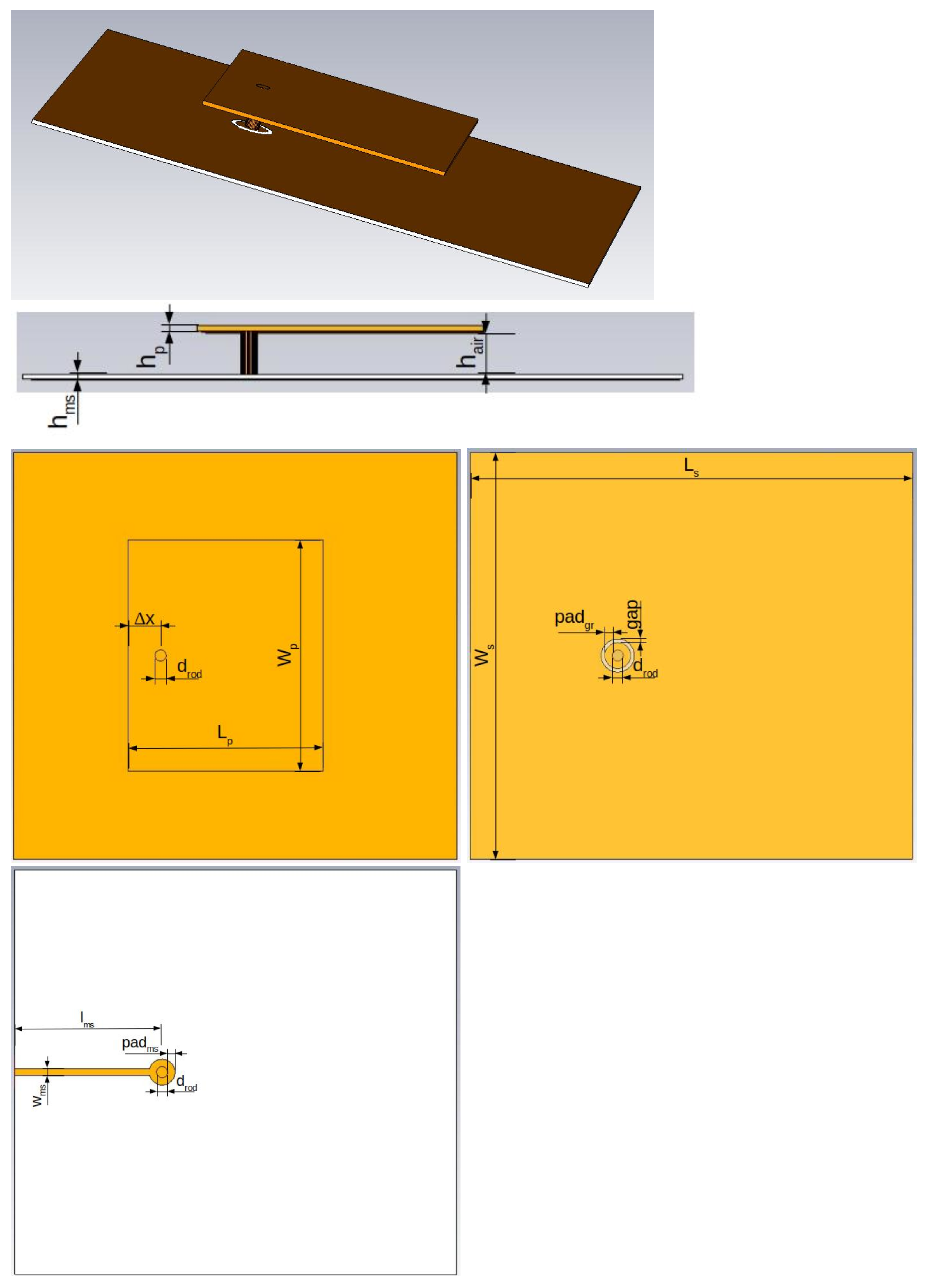
The appearance and design parameters of the prototype are illustrated in
Figure 1. The three parts composing the prototype are shown: the lower layer with a microstrip line whose ground plane is also used as the ground plane for the patch; the metallic floating patch optimized to radiate at 2.4 GHz; and the pin rod holding the patch and feeding it from the microstrip, whose insertion position and isolation from the ground plane are optimized to maximize the impedance matching.
The patch is just a completely metalized piece of Rogers-4003C of a thickness of 0.813 mm, giving a total thickness of
mm; its shape is a rectangle of the size
at the distance
over the ground of the microstrip layer. This distance is chosen to be
mm to ease the manufacture (it is the piling of ten substrates of a height of 0.813 mm). For a chosen radiation frequency of
GHz and the air as the patch dielectric (
), the design equations for the patch are simplified as follows:
where
mm is the size of the radiating edges (y axis),
mm is the size of the non-radiating edges (x axis),
is the effective dielectric constant (that matches
in this case), and
mm is the correction in size due to the fringing effects on the patch. The size of the patch reference plane (
) must be greater than the patch; it is recommended to be at least approximately the size of the patch incremented six times by the value of the dielectric (
,
).
The microstrip layer is integrated into an mm thick substrate of the size and mm with a 50 impedance microstrip line on the bottom side of the length mm and width mm. The top side of this layer is the common ground plane for the microstrip and patch.
The feeding of the patch is made with a coaxial probe that has been implemented as a pin rod connecting the microstrip line with the patch through the ground plane by using the through-wire technique stated in [
23]. With the aim of using the pin rod as the holding post of the patch, and considering the size of the patch, a 3 mm diameter metallic rod has been selected to ensure the robustness and stability of the device. To make the manufacturing process easier, the values of the pads and gaps necessary for the through-wire technique have been forced to the values of 1 mm for the gap in the ground plane and 2 mm for the pads around the metallic rod. As the rod must trespass the microstrip layer, a through-hole must be made; that hole needs to be metalized (with 9
m of copper electrodeposition) to achieve good connectivity with the rod, so that procedure needs to be completed before printing the microstrip line.
The insertion position of the pin rod into the patch is critical. According to the considerations stated in Chapter 21.6 of [
26], the insertion position for a linearly polarized antenna should be at the middle of one of the radiating edges and separated a distance
from the edge toward the center of the patch. It is well-known that the impedance strongly varies along the antenna, and, furthermore, the impedance and bandwidth are dependent on the ratio
because it changes the quantity of energy stored in the cavity formed by the patch and the ground plane. Consequently, it is stated in [
26] that the precise insertion position is very sensitive to
and
and only initial approximations can be given that must later be adjusted empirically through a simulator. Taking the former into account and considering that the air is the dielectric of the patch, the initial position of the insertion pin rod is estimated by
.
This device has been simulated (including losses), and the values of
and
(and therefore
) have been optimized for adjustment of the insertion position of the pin rod that maximizes the radiation at 2.4 GHz. The optimum point indicates that the antenna has a bandwidth of 10.46% around 2.4 GHz (according to the band with
dB), with a directivity of 9.95 dBi and a total efficiency of 99.78%; those values are quite promising, as they reflect the high-performance indexes of the bandwidth, efficiency, and gain at the same time for just a single radiating element. The final dimensions of the optimized device are those in
Table 1.
3. Results and Discussion
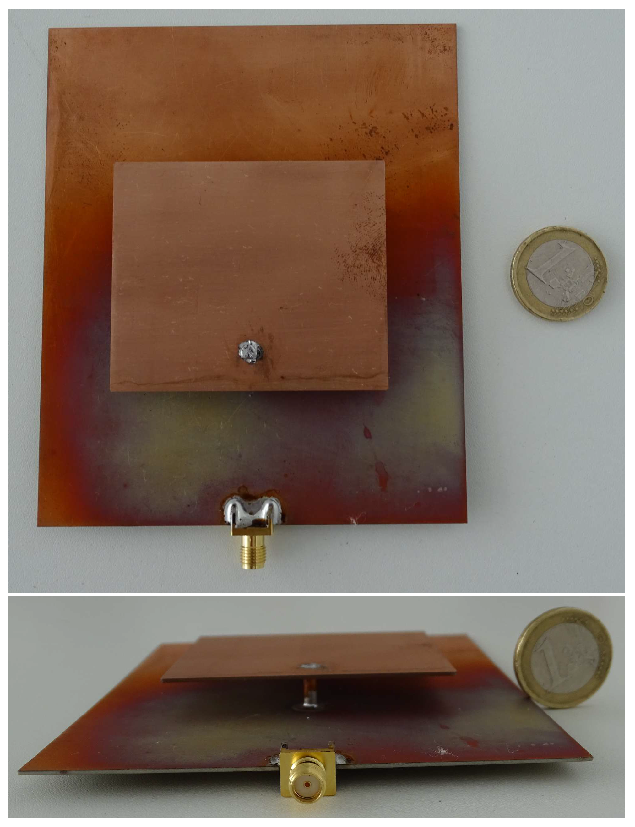
The designed device has been manufactured, and the resulting prototype is shown in
Figure 2. Just two pieces of the substrate are needed: one for the microstrip layer and another for the patch, apart from a short metallic rod to fasten both layers. The manufacturing process is quite simple and can be completed with standard PCB operations, such as drilling, cutting, milling, plating, and soldering. The hole for the rod is drilled into both substrate pieces. Then, the microstrip layer is plated to metalize the hole. Afterward, the microstrip line is printed, and the final layer is cut. On the other hand, after drilling the patch layer, it is directly cut and completely plated. Next, the rod is cut to the desired length, and it is tin-soldered to the patch. Finally, the rod has to be carefully soldered to the microstrip layer.
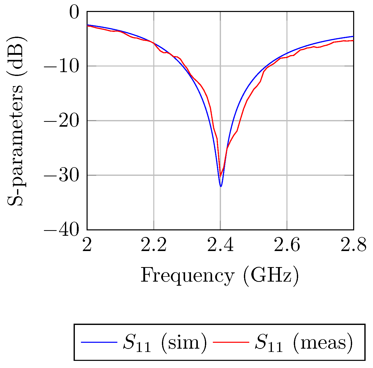
The prototype has been measured with a vector network analyzer (Agilent N5230C) to characterize the
parameter. The result is shown in
Figure 3, which compares the measurement to the simulation. It reflects practically a total match between the simulated device and the manufactured prototype; the measured return loss is 30 dB at 2.4 GHz with a measured bandwidth of 10.41% around the resonance frequency. This fulfills one of the goals of achieving a high bandwidth for the patch antenna by using the air as a dielectric and a through-wire feed.
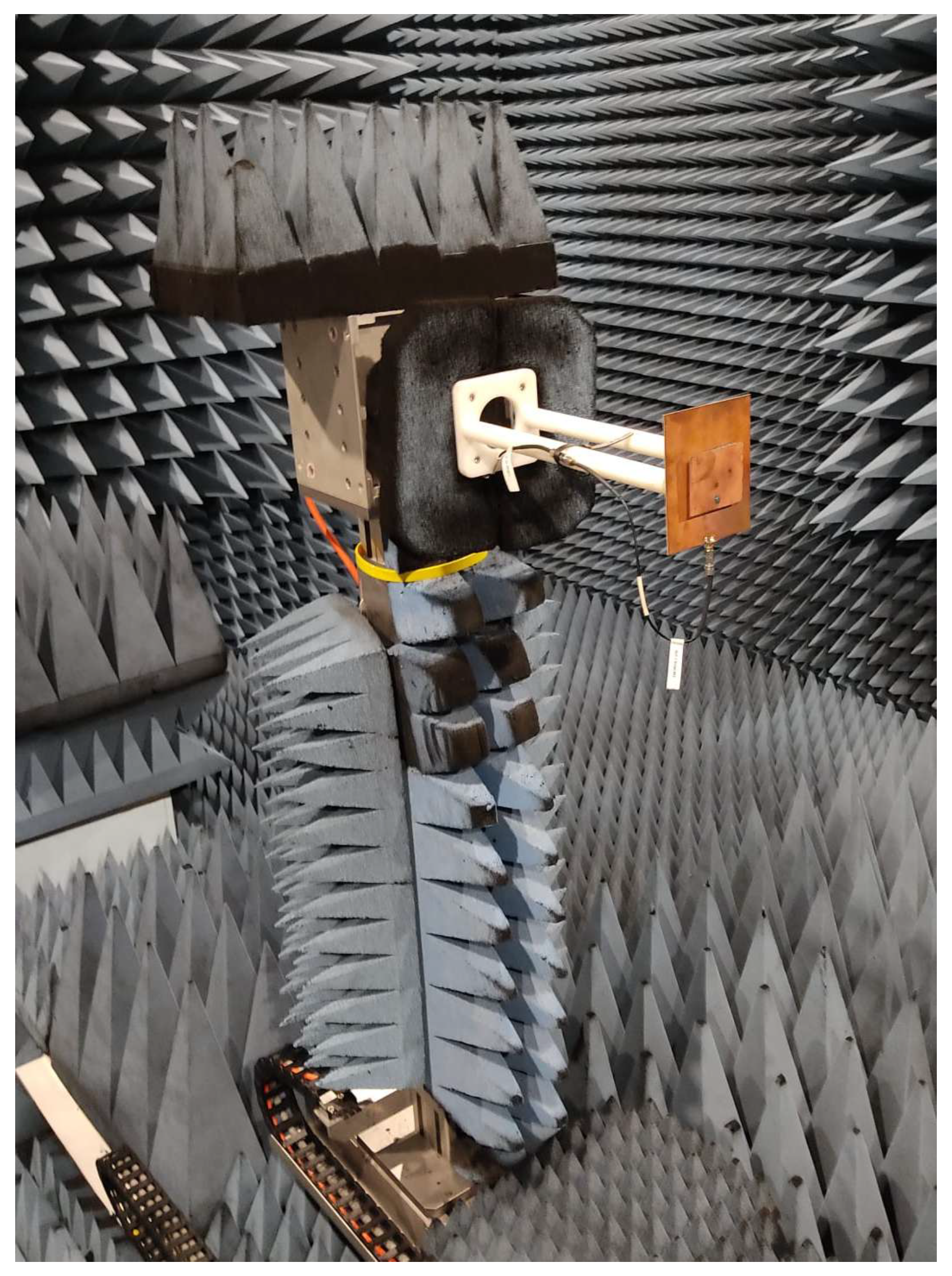
The radiation of the prototype patch antenna has been also measured in an anechoic chamber with the technique of the reference antenna (QRH500, in this case), as can be seen in
Figure 4. With the data acquired in this measurement procedure, the antenna can be completely characterized.
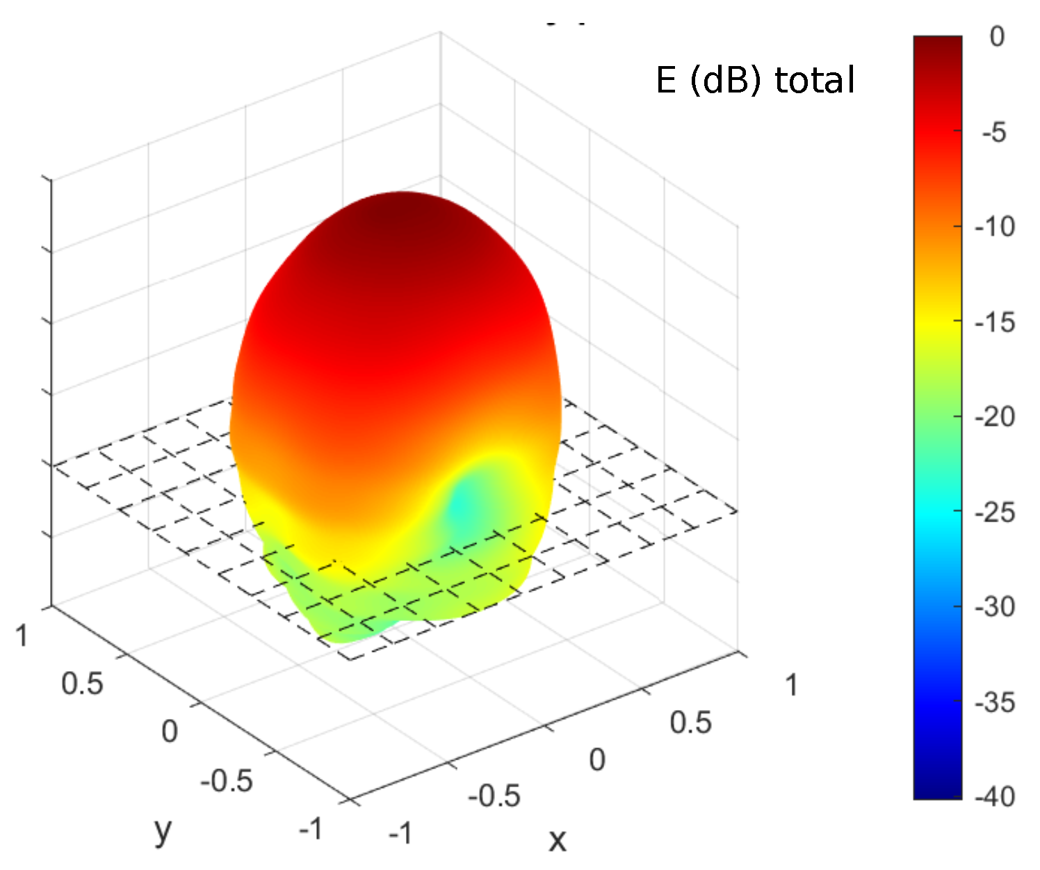
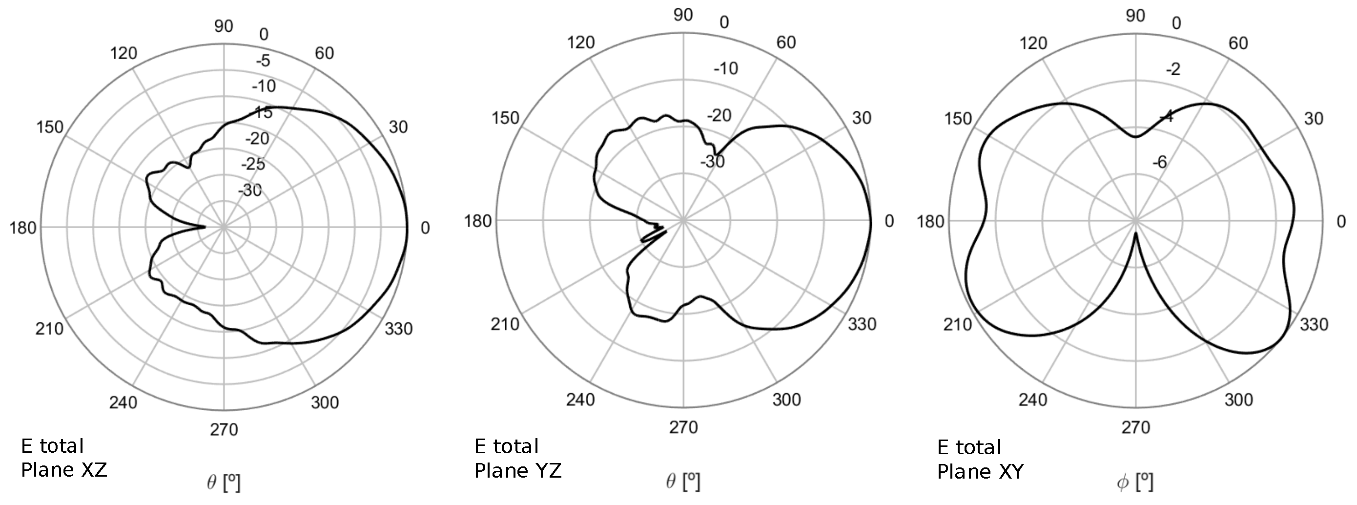
The measured radiation pattern is shown in
Figure 5, whose XZ (
), YZ (
), and XY (
) plane cuts are included in
Figure 6. The obtained patterns are typical of a patch antenna. The measured directivity at the resonance frequency is 9.94 dBi, with a measured gain of 9.63 dBi, which gives a radiation efficiency of 96.41% and a total efficiency of 93.08%. The maximum direction of the radiation is
and
, whereas the −3 dB beamwidth is
for plane YZ and
for the XZ. Moreover, a good cross-polar rejection is obtained, with 67 dB for the polarization ellipse axial ratio. These results fit almost perfectly with the simulations and reveal, as intended, the simultaneous high-performance indexes of the return loss, bandwidth, beamwidth, gain, and efficiency.
Despite the quite easy manufacturing process for this antenna, some inherent fabrication errors may occur. A yield analysis has been performed to check the endurance and repeatability of the proposed prototype and its manufacturing. It has been considered that errors may appear in the most critical operations: the milling pads and gap for the rod as well as the drilling position for the rod in the patch and the cutting process for the size of the patch. The selected criteria to mark a device as acceptable are that dB at a minimum bandwidth of 10% around the resonance frequency. Taking into account that the tolerance of the laser cuts used is 2 microns, the analysis indicates that, even for high tolerances of 25 microns, 100% of the devices would be acceptable. If the tolerance were extremely high, for instance, 50 microns, 99% of the prototypes would be acceptable; even for the unlikely case of an excessively high tolerance of 100 microns, 96% of the prototypes could be still acceptable. This reveals the accuracy of the design and the high tolerance for manufacturing errors of this prototype.
The results above prove the feasibility of this prototype and validate the simplicity and endurance of its fabrication procedure. To contextualize this new patch antenna device, the performance indexes of different air substrate microstrip patch antennas with just one radiating element are compared in
Table 2 regarding the resonance frequency, the return loss, the fractional bandwidth, the gain, the efficiency, and the feeding technique; qualitative aspects about the manufacturing complexity and other details of the prototypes are also included. The data in the table show that every published antenna can stand out in one or two performance indexes, and it also clearly reveals that this new antenna is the only one that is simultaneously completely dielectricless, able to achieve good values at the same time in all of the performance indexes, very easy to manufacture, and uses just one holder for both feeding the patch and fixing its position. The same happens if this antenna is compared with other patch antennas using different substrates, such as those in the compilation included in [
27].
4. Conclusions
In this paper, the design, fabrication, and measurement of a floating patch antenna are proposed. The design procedure is eased by selecting air as the dielectric for the patch, as well as a simple patch shape; the most critical aspect is the positioning of the feeding pin rod that connects the microstrip line to the patch so that there is a good impedance matching able to maximize the radiation at the resonance frequency. The manufacturing processes are standard PCB operations, and the whole fabrication procedure is very easy and highly tolerant of manufacturing errors. This antenna is able to radiate at 2.4 GHz with a 10.41% fractional bandwidth, 9.63 dBi gain, 96.41% radiation efficiency, and total efficiency of 93.08%, together with a wide beamwidth and good polarization purity. Thanks to the microstrip and through-wire feeding system, this antenna presents a high integration capability with other planar circuits; at the same time, this device is low-cost, lightweight, robust, and easy to manufacture. The main novelties of this design are its ease of design and manufacture, the total absence of a dielectric, the use of the through-wire technique to feed the patch and fasten the floating patch, the extreme robustness and error tolerance of the prototype, and the simultaneous achievement of good values in all of the performance indexes. The proposed antenna can be profitably used for wireless applications in the 2.4 GHz band.


 ,
, 


