1. Introduction
Single Event Upsets (SEU) have increasingly become a reliability concern for storage cells, such as Flip-Flops (FF), within Integrated Circuit designs (IC) [
1]. While common in space, SEU occurrences on the ground have also been documented [
2]. Electronic systems operating in environments with elevated radiation levels, such as space or high altitudes, should be hardened to limit the effects caused by ionized particle strikes [
3]. When an ionized particle with sufficient energy strikes a sensitive region of a storage cell, it can cause the contents of the cell to become flipped. As feature sizes of transistors continue to scale down, the likelihood of SEUs within complex designs is expected to increase due to the smaller amount of deposited charge needed to cause an upset [
4,
5].
Over the years, various techniques have been used to harden storage cells. These techniques may be performed at the schematic level of the cell or in the physical layout. One such design that has proved to be effective at preventing SEUs is the Dual Interlocked Cell (DICE). This design provides single-node upset immunity due to the interlocking of four back-to-back inverters [
6]. However, at sub-micron bulk technology nodes, such as at 65 nm, 40 nm, or 28 nm nodes, the Soft Error Rate (SER) performance of the cell becomes less effective. This is because at these scales, the spacing between adjacent transistors is small enough that deposited charge clouds from ion strikes can often affect more than one transistor at a time. This charge-sharing phenomenon renders the DICE cell to be ineffective at preventing SEUs [
2,
7]. While it is possible to reduce the charge sharing effect in bulk technologies through a smart layout design, as shown in [
8], these alterations can come with increased area and performance penalties, as well as increasingly complex metal layer routing. Furthermore, it is not yet definitive if these layout changes can still make DICE effective at bulk nodes smaller than 28 nm. As such, the use of the Fully Depleted Silicon on Insulator (FD SOI) technology is attractive for DICE cells due to the limited charge sharing between adjacent transistors.
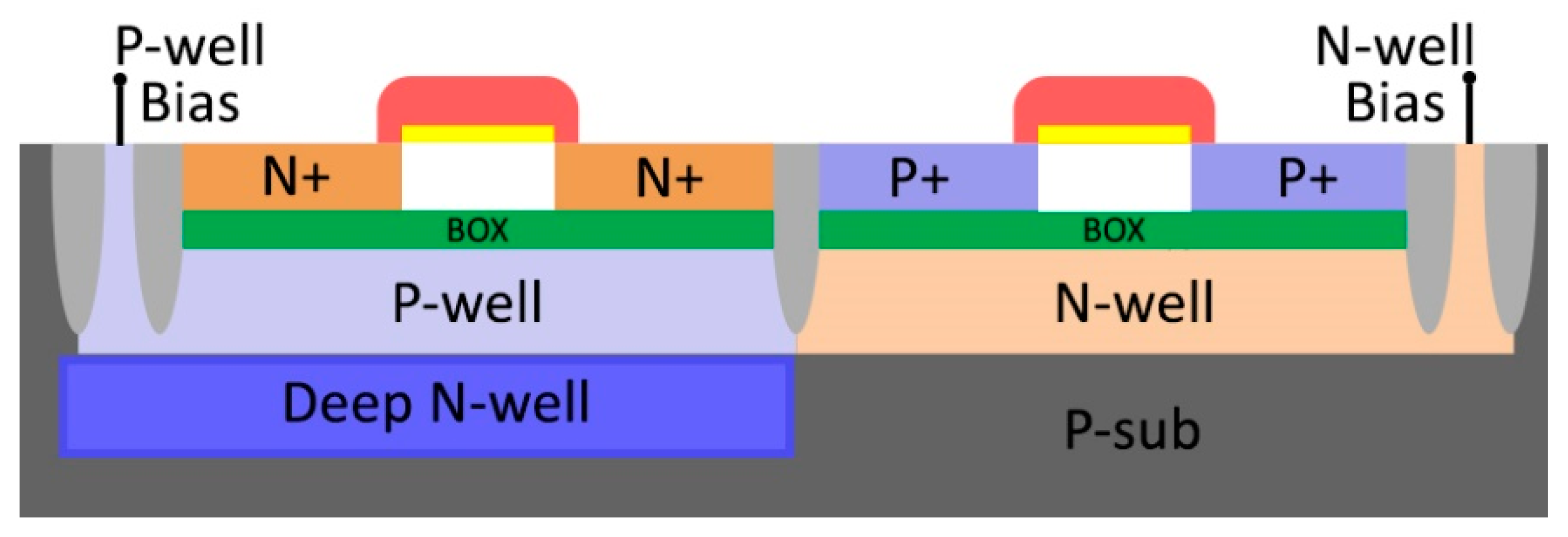
Transistors developed with the FD SOI technology are fabricated on a small silicon island on top of a thinly Buried Oxide (BOX) layer, as shown in
Figure 1. This provides various advantages over similar bulk technology nodes, but most notably, charge sharing between adjacent transistors is greatly reduced since each transistor is electrically isolated due to the BOX layer. Additionally, the amount of deposited charge from an ionized particle strike is decreased because of the small silicon island [
9]. As a result, flip-flop designs using DICE latches have once again become an effective way to reduce SEUs within IC designs. However, when using nano-scale technologies, such as in the case of 22 nm nodes, the spacing between adjacent transistors may be small enough that the isolation provided by the BOX layer is no longer sufficient to completely prevent charge sharing [
10]. Other techniques, such as guard-gate stacking, may be needed to further harden the DICE latch [
10]. Additionally, the 22 nm FD SOI technology node allows for a new layout construct known as Continuous Active Diffusion (CnRx) [
11]. This construct aims to remove the channel strain on PFETs by replacing any PFET active diffusion breaks with a special type of layout structure to produce an uninterrupted diffusion region. It is not yet fully known how this new construct will affect the soft error rates of hardened cells, such as DICE.
From 28 nm node data, a conventional master–slave FF using back-to-back inverter latches in the FD SOI technology can potentially rival the SER performance of a hardened DICE design at a similarly sized bulk technology node [
12,
13]. The performance of DICE at the 22 nm FD SOI node has not yet been fully evaluated, and more research should be performed to understand the impacts of node interleaving, guard-gate stacking, and the new CnRx construct; CnRx is likely to be used in many complex logic designs.
In this article, four different FFs, including three DICE designs, are proposed and were fabricated on a 22 nm FD SOI test chip. Alpha particle and heavy ion irradiation experiments were conducted to evaluate the SEU sensitivity of all designs. The novelty of the DICE designs is the use of transistor interleaving in the layout of the latches to further harden them against SEUs. These results can provide increased understanding of the efficacy of DICE designs at nano-scale technology nodes, as well as insights into the effects of transistor stacking as well as the CnRx Construct. The CnRx layout construct has not yet been studied for DICE designs at the 22 nm FD SOI technology node.
The rest of the article is organized as follows:
Section 2 introduces the proposed designs, and
Section 3 presents the experimental results and simulations. A discussion of the data is provided in
Section 4, before concluding remarks are presented in
Section 5.
2. Materials and Methods
A standard FF was designed to act as reference when comparing data between the proposed DICE designs. This reference design used master and slave latches with clocked transmission gates, as shown in
Figure 2.
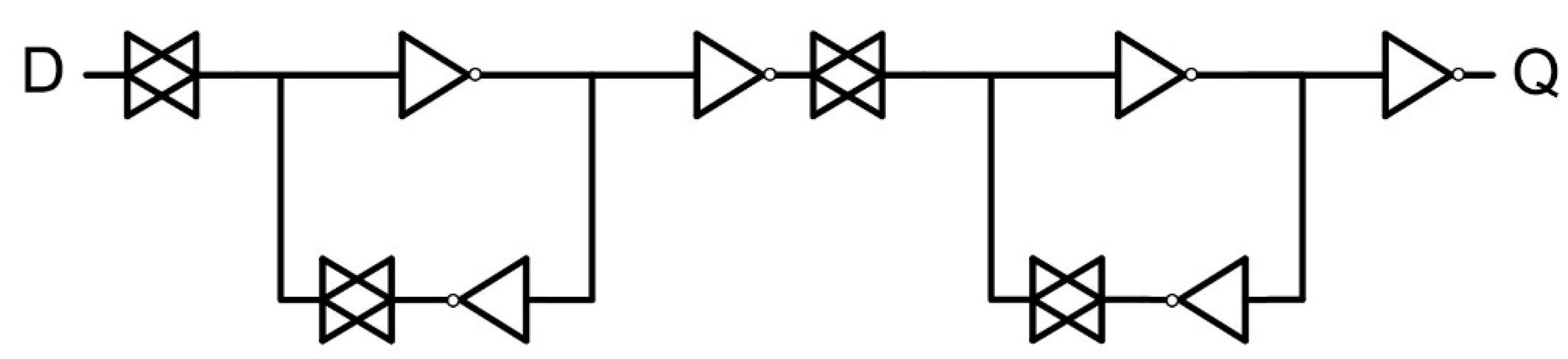
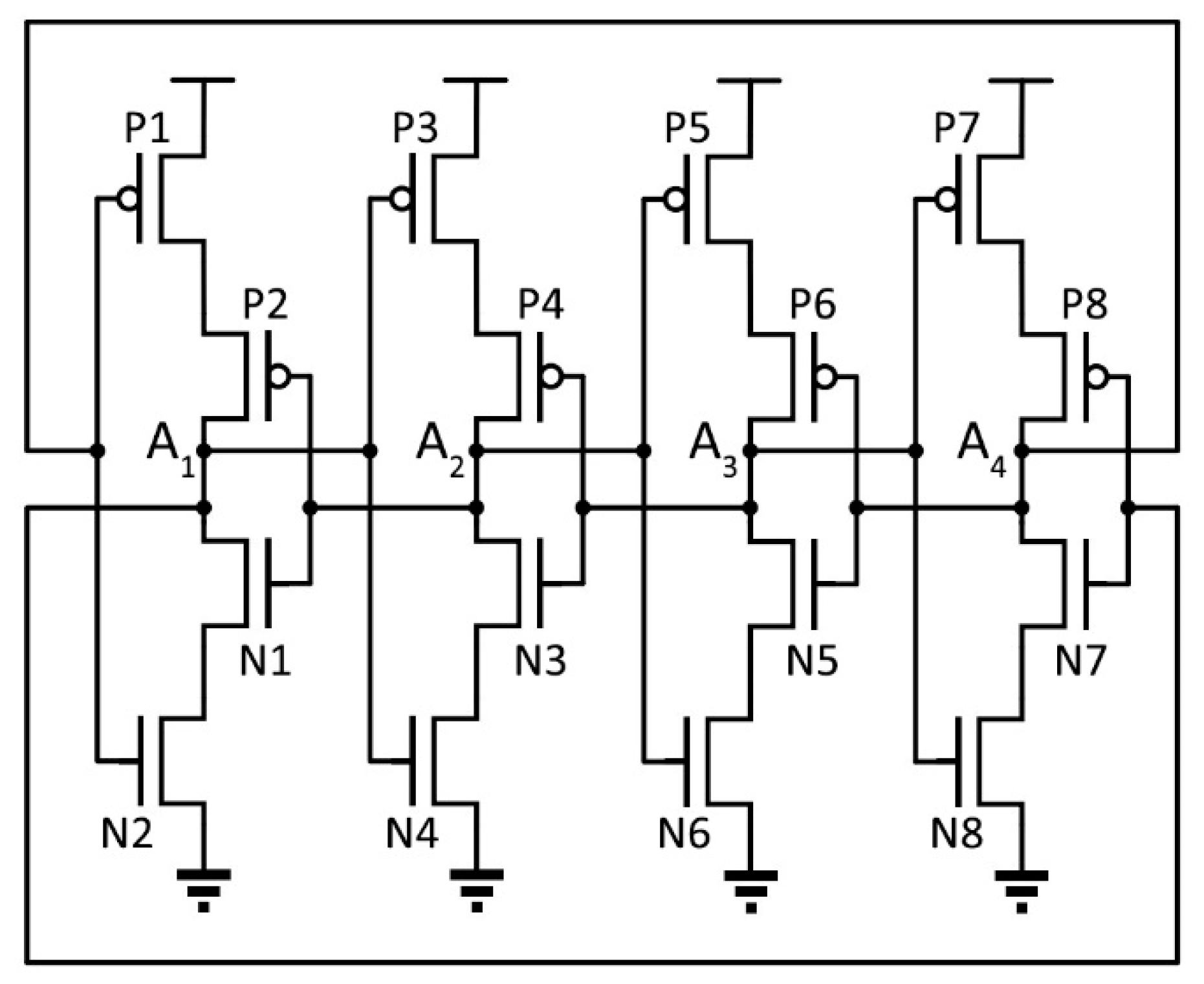
The latches used in the reference design were standard back-to-back inverters. The proposed FF designs presented in this paper used a similar master–slave design, except that in each DICE design, the back-to-back inverter latches were replaced with the respective DICE latches. Note that DICE stored both the original data and the complemented version of the data in the cell. Nodes A1 and A3 stored the uncomplemented data, whereas nodes A0 and A2 stored the complemented version. In the design of DICE-based FFs, both versions of the data need to be available so to be written into the cell; therefore, the flip-flop designs were modified with the addition of extra transmission gates and. A schematic of the DICE flip-flop design is shown in
Figure 3.
The figure above shows the DICE schematic that all three proposed designs in this work followed. Note that for the three proposed designs, any changes were only introduced in the DICE latch and not in the rest of the flip-flop circuitry. As previously discussed, DICE has intrinsic single-node upset immunity due to the inherent interlocked feedback loops present within the circuit. However, the charge track caused by a single ionized particle could still affect two or more adjacent transistors when the spacing between adjacent devices is small enough, even for the FD SOI technology. This scenario could worsen with angular particle strikes that are likely to impact more than one transistor at a time. For example, if nodes A1 and A2 are placed next to each other in the layout, an angular particle strike could cause a SET at both nodes, thus flipping the data stored in the cell. It is therefore beneficial to add additional hardening techniques to a DICE design.
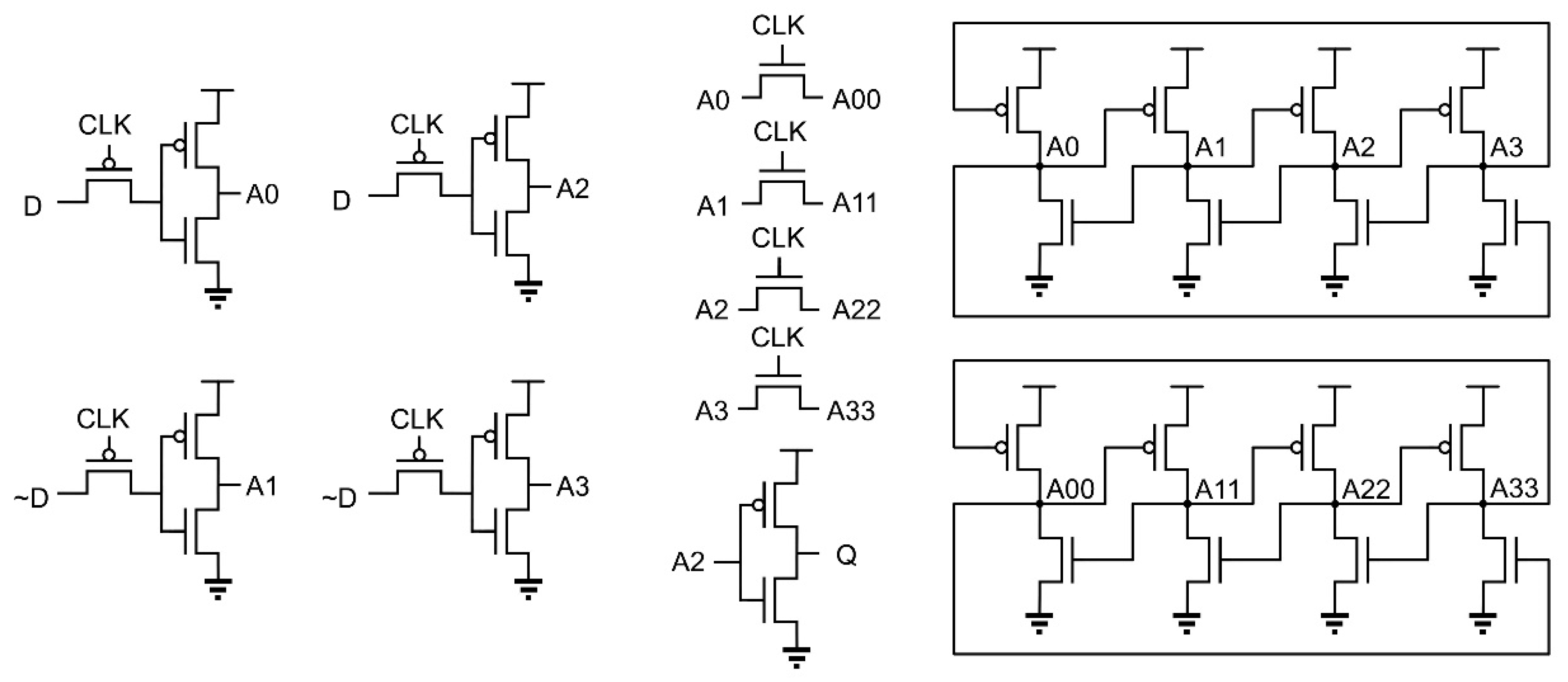
Transistor interleaving purposely separates transistors that share a common input to different location in the layout to help prevent multiple sensitive nodes from being struck at the same time. Only a particle with a sufficiently large Linear Energy Transfer (LET) at a steep incidence angle would be able to strike both nodes. This type of layout hardening does make the routing of metal layers slightly more complex, but the performance penalties are expected to be limited. Shown in
Figure 4 is a comparison between a non-interleaved DICE latch design and an interleaved design. In the interleaved design, the second and third inverters were swapped to increase the distance between sensitive nodes. In real designs, the actual spacing between adjacent sensitive nodes may be larger or smaller depending on the inclusion of other logic elements or other layout changes. All presented DICE designs in this article made use of the interleaved layout shown in
Figure 4b.
The 22 nm FDSOI technology node makes use of Embedded Silicon Germanium (eSiGe) in the channel of PMOS transistors to help enhance their performance [
14]. However, the Length of the Oxide (LOD) diffusion can reduce the performance benefits gained by the inclusion of the eSiGe. When the lengths of the active diffusion layer on each side of the gate of the device are too short, the mobility of holes becomes reduced [
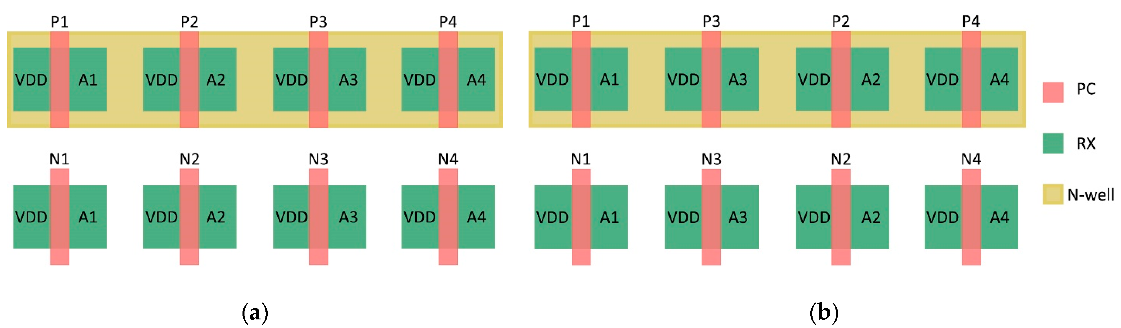
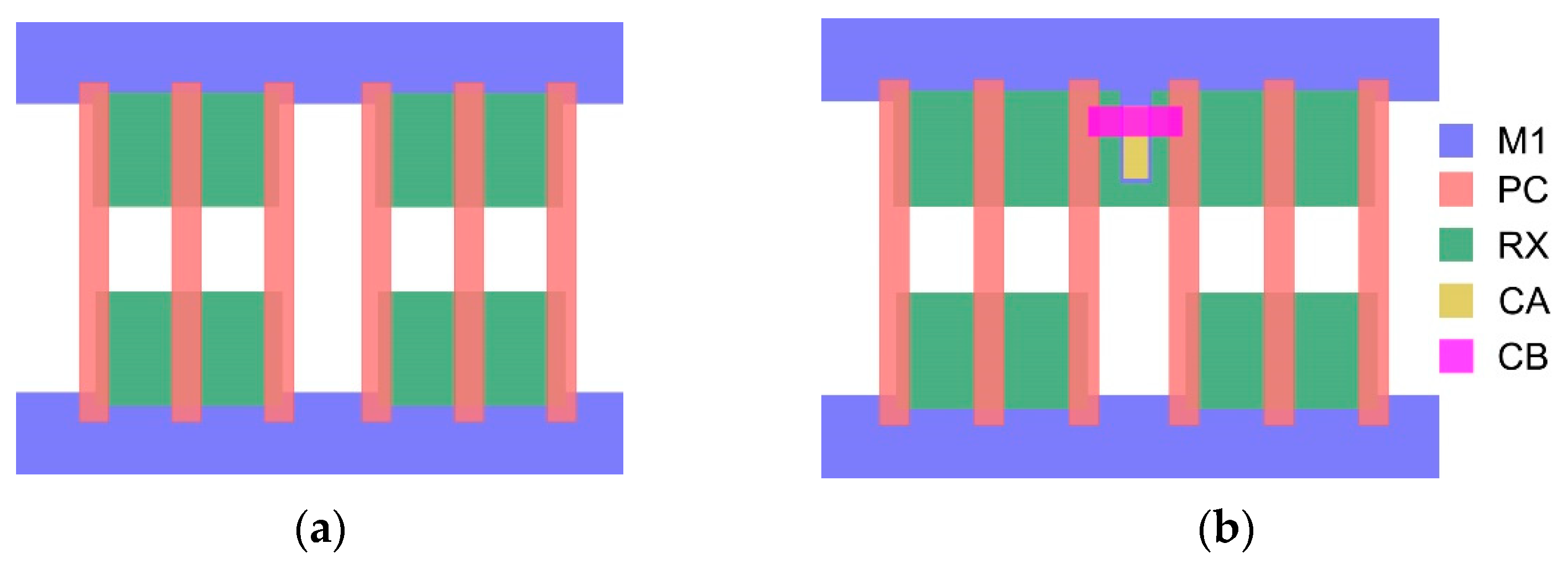
15]. In order to have competitive standard cell designs for dense logic applications in the 22 nm FD SOI node, the Continuous Active (CnRx) diffusion construct can be used. In this construct, the active diffusion layer for PFET devices in a standard cell are kept continuous with no breaks in the layout. This helps retain the performance benefits that eSiGe offers. To achieve this, adjacent transistors that would otherwise be separated by dummy polysilicon are replaced with special T-shaped or L-shaped structures, as shown in
Figure 5. These special structures tie dummy polysilicon to their respective VSS or VDD lines and allow the active diffusion layer to be made continuous. Early results showed that the CnRx construct can offer 30% performance benefits over traditional Single Diffusion Break (SDB) or Double Diffusion Break (DDB) designs [
11]. Additionally, due to simplified masks for fabrication purposes, CnRx can also provide increases in cell density.
The proposed DICE FF design in this work making use of the CnRx construct used the same interleaving layout technique that was previously described. To provide the best possible comparison between the other designs and the CnRx DICE FF, no changes were made to either the schematic or the layout of the design other than the use of the special T-shaped and L-shaped structures to make the active diffusion layer of the PMOS transistors continuous.
The guard-gate technique can be used in latch designs to help mitigate soft errors. In the guard-gate hardening technique, two input signals are compared such that the circuitry will be able to operate as normal if they are the same; in contrast, if the inputs differ, the guard gate causes the output of the circuitry to remain the same. Shown in
Figure 6 is the guard gate DICE latch presented in this work.
The effectiveness of transistor stacking has been proven in the 28 nm FD SOI technology node due to the isolation between transistors, and the guard gate technique takes advantage of this due to its inherent stacking structure [
16]. The guard gate structure is very similar to that of a stacked transistor structure, the key differentiator between guard gating and transistor stacking being that in transistor stacking, the two series transistors share the same input. In the guard gate DICE latch, their inputs are connected to two separate nodes storing the same data. For example, if node A
1 currently stores a ‘0’, then the adjacent nodes A
3 and A
2 will store a ‘1’, thus keeping off the two PMOS transistors of the first inverter. This helps prevent a SET pulse from affecting the two series transistors simultaneously, since a pulse on one node will only affect a single transistor of a stacked inverter. The 22 nm FD SOI node is expected to follow the same SER improvement trends as the 28 nm FD SOI node when it comes to guard gating and transistor stacking. However, if both series transistors in a stacked structure are struck simultaneously by a particle with a steep incidence angle causing current pulses in both transistors, then the benefits of transistors stacking are lost. In the guard gate DICE FF design, the minimum distance between two sensitive nodes was 0.42 µm.
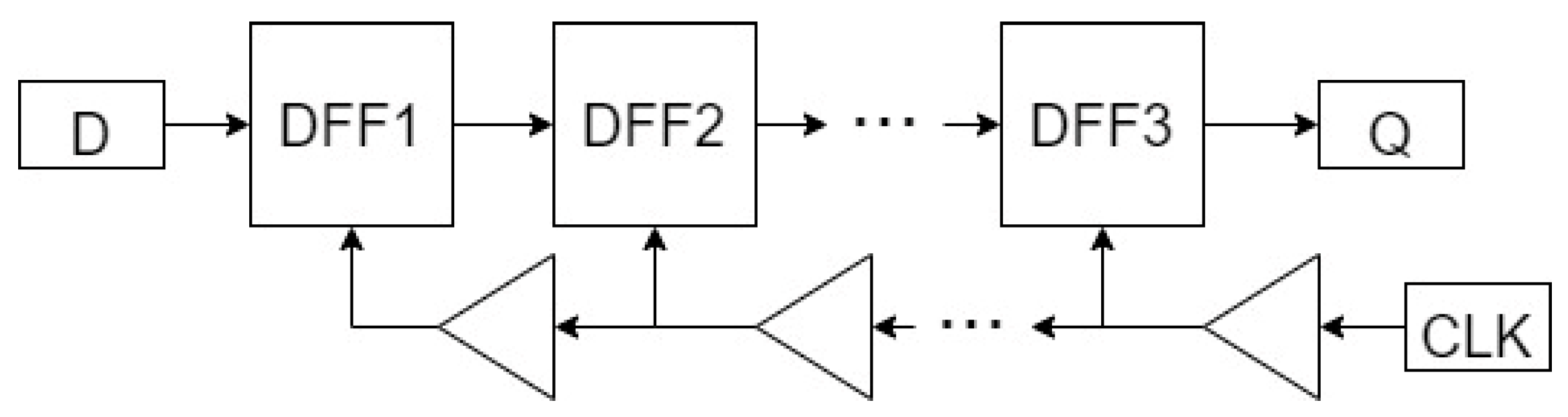
The three DICE FF designs, the standard interleaved DICE, CnRx DICE, and the Guard Gate DICE were fabricated on a 22 nm FD SOI test chip alongside the reference FF. The FF designs were placed into shift register chains containing 11,700 serially connected FFs and were clocked using the reverse clocking scheme. This clocking was used to help alleviate any potential issues with hold time violations or clock skew in the chains during testing.
Figure 7 shows the block diagram for an implemented chain in the test chip. The nominal core voltage for this technology is 0.8 V, and the I/O voltage used was 1.8 V.
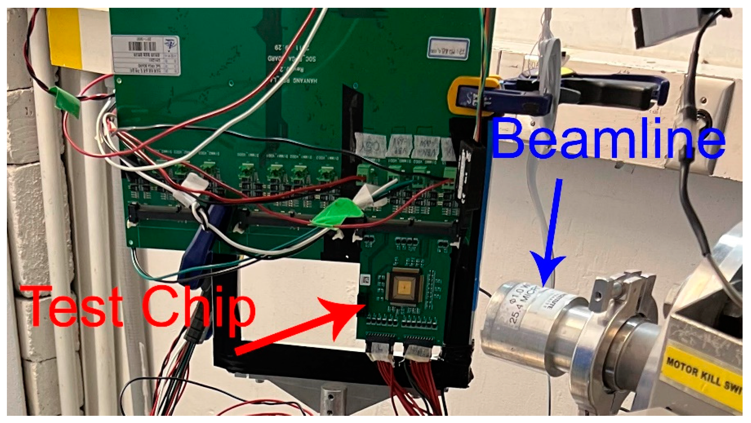
To monitor for SEUs, a test system consisting of power supplies, a FPGA board, and a microcontroller was used. The FPGA board controlled the external clocking of the chains, the data input to the chains, as well as the error detection. The test chip was soldered onto a custom-made PCB board that allowed for access to all pins on the chip via a DIMM connection. During testing, at each positive clock edge, if the output of a chain did not match the input, then a SEU was recorded, and a respective register within the FPGA system was incremented. The data in each of the registers storing the number of upsets for each chain were then transmitted to a microcontroller where they were then logged and recorded in real time. The data were transferred using a serial protocol. During all tests, the chains were clocked at a frequency of 1 MHz, and the ‘all 0’ data pattern was used.
Before the experiments were conducted on the test chip, each chain’s functionality was validated by a series of tests. Input data of all 1 s, all 0 s, and alternative 0 and 1 patterns were inputted to the chain, and the outputs were observed to ensure that the proper data passed through the chains. In addition, the error capture system was validated by injecting voltage pulses onto the chains via the pins of the chip, and subsequent errors were noted on the test system. Additional checks were completed by injecting errors into the chains via the FPGA testing system. As such, all proposed chains functioned as expected, both before and during testing.
4. Discussion
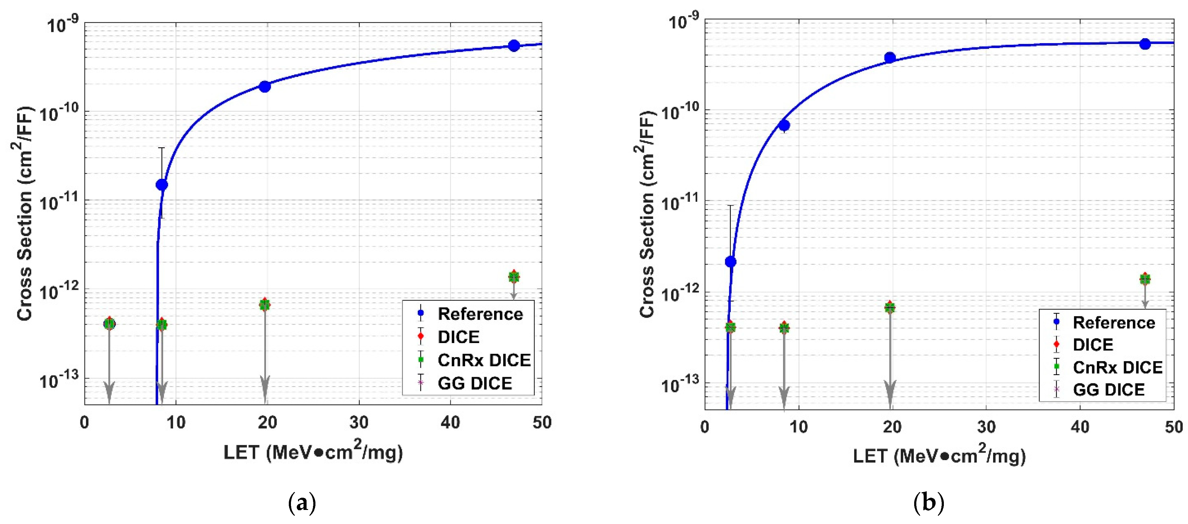
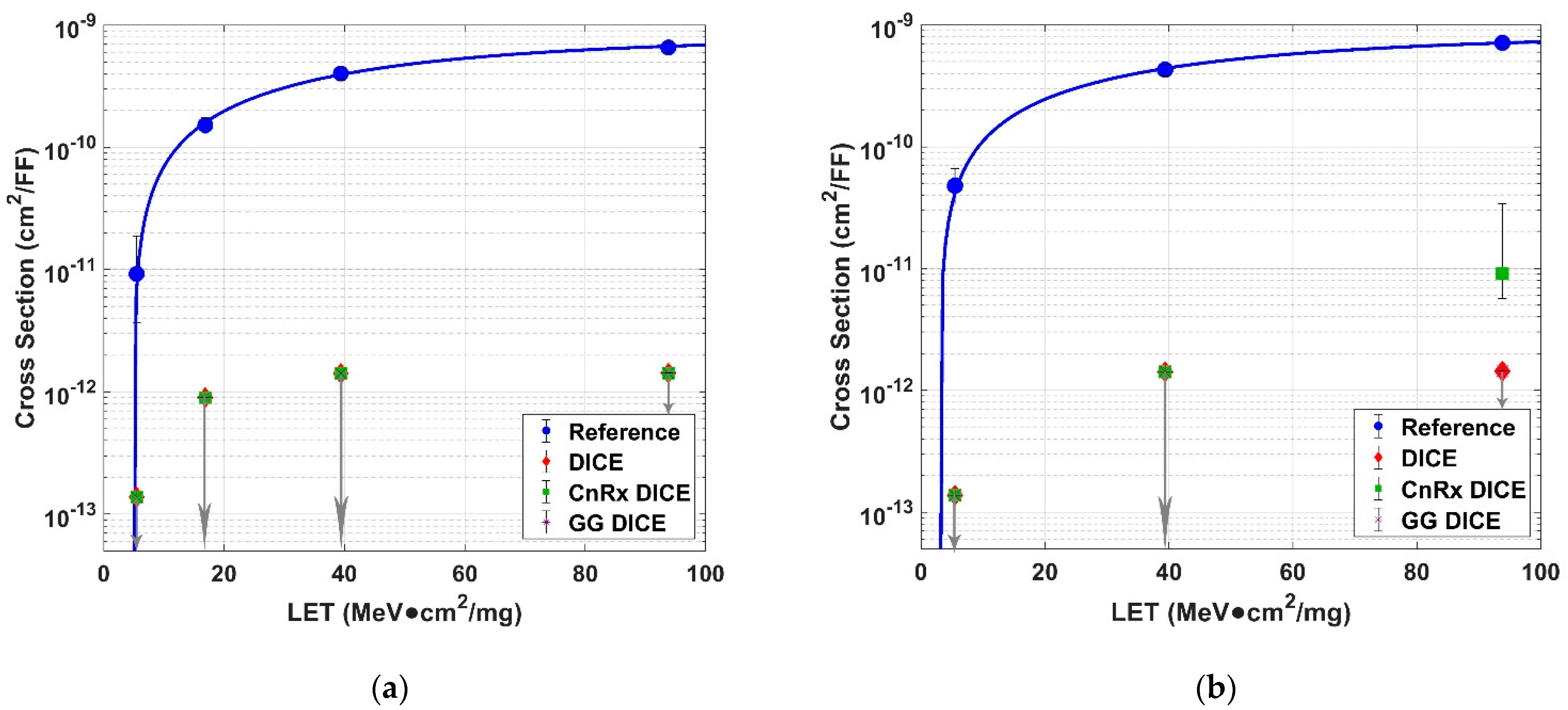
As shown by the experimental data, the use of transistor interleaving for DICE-based FF designs at the 22 nm FD SOI technology node showed superior SER performance compared to a standard FF design. The normal DICE FF with transistor interleaving showed no upsets during any of the tests, including tests where ions impacted the test chip at an angle of 60° from normal. This showed that transistor interleaving can effectively mitigate SET pulses from occurring simultaneously on two sensitive nodes. There is no doubt that singular upsets occurred on individual nodes of the DICE cell; however, these upsets made no impact on the cell due to the intrinsic single-node immunity of DICE. Additionally, the Guard Gate Stacked DICE FF presented no errors either. This was expected, since if the regular DICE FF design showed no errors, then the guard-gate design should show no errors either because of its additional hardening techniques. As such, for DICE designs at the 22 nm FD SOI node, the use of guard gating is not needed to protect cells from SEUs, given that the sensitive nodes are properly spaced apart.
The CnRx DICE DFF was the only design that presented upsets during testing. The upsets were observed with a high-LET ion at both a steep incidence angle and a reduced core voltage. This data showed that DICE designs making use of the new CnRx are slightly more likely to experience SEUs. However, since the upsets were only recorded in these extreme conditions, it is likely the construct has a little effect on DICE. As such, designers will have to take into consideration this cost of increased performance depending on the use cases of their designs. DICE FFs at the 22 nm FD SOI node performed well, regardless of what layout construct was used.
Based on DICE data available for a 28 nm bulk technology node as presented in [
17], the interleaved FD SOI DICE designs presented in this work showed superior SER performance. This improvement can largely be attributed to the natural electrical isolation that the FD SOI technology provides, since with bulk technologies, the charge-sharing phenomena will largely impact the SER. However, FD SOI DICE designs not making use of transistor interleaving are still susceptible to upsets, as shown in [
18]. Thus, from the results, it can be concluded that the usage of transistor interleaving for DICE FFs at the 22 nm FD SOI technology node provides extremely robust resistance to radiation-induced soft errors.


