
Arrays of TiO2 Nanosphere Monolayers on GaN-Based LEDs for the Improvement of Light Extraction

1
Department of Electronic Engineering, Hanyang University, Seoul 04763, Republic of Korea
2
Division of Nanosemiconductor Engineering, Hanyang University, Seoul 04763, Republic of Korea
*
Author to whom correspondence should be addressed.
Appl. Sci. 2023, 13(5), 3042; https://0-doi-org.brum.beds.ac.uk/10.3390/app13053042
Submission received: 19 January 2023
/
Revised: 16 February 2023
/
Accepted: 24 February 2023
/
Published: 27 February 2023
(This article belongs to the Special Issue Advanced Compound Semiconductor)
Abstract
:We report on the fabrication of TiO2 nanosphere (NS) monolayer arrays for the enhancement of light extraction quantum efficiency of GaN-based light-emitting diodes (LEDs). The fabricated TiO2 NSs monolayer arrays were composed of different phases of anatase (An-) and amorphous (Am-) TiO2. The arrays were transferred onto the topmost layer of LED chips via the facile icing transfer method. The LED chips covered with Am-TiO2 NS monolayer arrays showed 3.0- times enhanced light output power intensity compared with reference LED chips at a fixed injection current of 100 mA. The enhanced light extraction of LED chips by an Am-TiO2 NS monolayer can be attributed to a high transmittance (91.1%) in visible and increased light extraction probability of photons generated in LEDs, resulting from the enhanced light coupling efficiency by reduced total internal reflection (TIR). Finite-difference time-domain (FDTD) simulation results also agreed well with the experimentally observed results. Based on the experimental and theoretical results, our suggested Am- and An-TiO2 NS arrays can be considered a very facile and effective method to improve the device performance of various visible LED chips.
1. Introduction
Titanium dioxide (TiO2) has received a great deal of attention for its various applications in solar cells [1], gas sensors [2], photodetectors [3], lithium-ion batteries [4], and other optoelectronic devices [5] due to its superior properties such as chemical stability [6], high photocorrosion resistance [7], and non-toxicity [8]. Among the versatile applications of TiO2 nanostructures for light generation and guiding, diverse surface morphologies such as nanoparticles [9], nanotubes [10], nanowires [11], submicron/nanospheres [12,13], and mesoporous structures [14] have been extensively investigated. For light extraction enhancement of GaN-based light emitting diodes (LEDs) to achieve high quantum efficiency, TiO2 nanomaterials, including micro-pillars [15] and nanopatterns [16], have been especially suggested as potential candidates for light extractors that minimize the total internal reflection (TIR) due to their wide band gap (~3.5 eV at room temperature) [17], high transmittance (~90%) [18] in the visible region, and refractive indices (n = 2.8 for the anatase phase and n = 2.5 for the amorphous phase) intermediate to those of GaN and air [19].
Recently, the utilization of metal oxide nano- and microsphere-type nanostructures has been reported to augment the light extraction efficiency of LED chips [20,21]. Such nanostructures offer advantages such as the ease of formation of arrayed nano- and microspheres via a simple transfer method [22]. Previous reports used a poly vinyl alcohol (PVA) attaching layer to transfer the monolayer array. The use of PVA can, however, degrade the reliability and efficiency of the LED chips because thermal damage can occur with the long annealing process at high temperatures necessary for the removal of PVA [23]. Therefore, to universally use the transferrable metal oxide micro/nanosphere monolayer without limiting the substrate material, the reduction of post-thermal annealing damage is an essential issue. Among the possible methods, the icing transfer method may be a good candidate because during processing, it uses deionized (DI) water as a binder with a soft baking temperature and short time (60 °C/ 30 s), none of which causes severely harmful effects, such as the deformation or degradation of the device.
In this study, we fabricated a uniformly arrayed TiO2 NSs monolayer with different crystal structures of amorphous (Am-TiO2) and anatase (An-TiO2) and transferred them onto the LED chips to enhance the light extraction efficiency. The formation of the ordered TiO2 NS monolayer array and its transfer were conducted by a simple unidirectional rubbing method and icing transfer method assisted by DI water. Our transferrable TiO2 NS monolayer arrays can be an excellent way to improve the device performance of LED chips. The experimental and finite-difference time-domain (FDTD) simulation-based theoretical results confirmed that the Am-TiO2 NSs monolayer enhanced the extraction efficiency of LED chips.
2. Materials and Methods
For the fast synthesis of TiO2 NSs, we used a solution process method. First, we mixed acetonitrile 40 mL, ethanol 50 mL, methylamine and H2O solvents with magnetic stirring (Solution A). Ethanol 10 mL and titanium isopropoxide (TTIP) solvents were mixed with magnetic stirring (Solution B). Solutions A and B were mixed together in a 250 mL round bottom flask at room temperature for 1H. TiO2 NSs were collected by centrifugation and washed with DI water. TiO2 NSs were then dried in an oven at 80 °C. The obtained as-synthesized amorphous TiO2 (Am-TiO2) NSs were converted to anatase TiO2 (An-TiO2) NSs through thermal treatment at 450 °C for 4 h.
Structural properties of the synthesized amorphous TiO2 (Am-TiO2) and anatase TiO2 (An-TiO2) NSs were investigated by scanning electron microscopy (SEM) (S-4800, Hitachi, Tokyo, Japan), and a high-resolution X-ray diffraction (HR-XRD) system (SmartLab, Rigaku, Tokyo, Japan) equipped with Cu-Kα radiation (1.54 Å). Optical properties of the TiO2 monolayers were analyzed by ultraviolet–visible light (UV-vis) spectroscopy (Lambda 650S, Perkin Elmer, Waltham, MA, USA). To evaluate the light extraction and electrical properties of the LED chips with TiO2 NSs monolayers, light output power–current–voltage (L–I–V) measurements were conducted (Keithley 2400, Tektronix, Beaverton, OR, USA).
GaN-based LED epi-structures were grown on a c-plane sapphire substrate via metal–organic chemical vapor deposition (MOCVD). Trimethylgallium (TMGa), trimethyindium (TMIn) and NH3 were used as the Ga, In, and N precursors, respectively. The LED structures consisted of a 1 µm thick unintentionally doped GaN layer, a 2 µm thick n-type GaN layer, six pairs on an InGaN/GaN multiple quantum well (MQWs) active layer, and a 0.3 µm thick p-type layer. The active layer consisted of six pairs, each with a 3 nm thick InGaN well layer and a 10 nm thick GaN barrier layer in the MQWs [24]. To fabricate the chip, blue LED wafers were partially etched by inductively coupled plasma (ICP) until the n-type GaN layer was exposed. Indium tin oxide (ITO, 100 nm) was evaporated to the surface of p-GaN for current spreading. Cr/Au electrodes (10/500 nm) were subsequently evaporated as both n- and p-type electrodes for contact metal. Finally, LED wafers were divided into chips with an area of 600 × 600 µm2.
3. Results
3.1. Transfer of TiO2 Nanosphere Monolayer onto GaN-LEDs
To form the TiO2 NS monolayer array, TiO2 NSs were formed on a PDMS pad with the elegant unidirectional rubbing method described in other references [25] and as shown in Figure 1a. Then, DI water was drop-cast on the surface of the LED chips, and a flipped TiO2/PDMS pad was placed on them (Figure 1b). After freezing the DI water for 10 min under −18 °C conditions, the PDMS pad was peeled from the LED chip (Figure 1c). The TiO2 NS structure left behind formed monolayer arrays on the LED chips, as displayed in Figure 1d.
3.2. Structural and Optical Characterization of TiO2 Nanospheres
The surface morphologies of Am- and An-TiO2 NSs synthesized by solution-based synthesis method are observed by SEM as shown in Figure 2a,b, respectively. Figure 2a,b shows the uniformly distributed sizes and morphologies of as-synthesized and calcinated TiO2 NSs. The average diameters of Am- and An-TiO2 NSs were measured as 498 ± 5 nm and 496 ± 5 nm, respectively, as depicted in the inset of Figure 2. The summary of the size dependence of TiO2 NSs with respect to the mixed solution ratio is depicted in Table S1. Generally, the solution-based synthesis of TiO2 NSs is governed by a hydrolysis process [26]. Initially, the stepwise hydrolysis forms primary TiO2 hydrates with sizes of a few nanometers, which have high surface energy and small electrostatic charges. Hence, TiO2 hydrates agglomerate spontaneously owing to van der Waals attractive forces and hydrogen bonding among the individuals [27]. As the mass of the TiO2 hydrates increases by gradual aggregation of the individual hydrates, the electrostatic charges build up in the aggregated TiO2 hydrates. When TiO2 spheres achieve a certain critical size, the repulsive interaction becomes sufficiently strong to block the Brownian aggregation, leading to each TiO2 sphere being completely separate and without further increase in size.
To investigate the phase conversion of the TiO2 spheres from as synthesized to after annealing at different temperatures, we analyzed the XRD patterns. Figure 3a shows the XRD spectra of the Am- and An-phase TiO2 NSs drop-casted on the Al2O3 substrate. For the Am-TiO2 NSs, there are no strong peaks in the XRD pattern, indicating that there is no crystallized phase, as shown (black line) in Figure 3a. By increasing the annealing conditions to 450 °C for 4 h, strong 2θ peaks appeared at the diffraction peaks placed at 25.2°, 37.8°, 48°, 55°, 62.6°, 70.3°, and 75°, which are well matched with crystal planes (101), (103), (200), (105), (204), (220), and (215) of An-structured TiO2 (JCPDS No. 21-1272), as shown (red line) in Figure 3a. According to the XRD results, we know that as-synthesized Am-TiO2 NSs changed to An-TiO2 via heat treatment [28].
Transmission electron microscopy (TEM) images further reveal that the Am- and An-TiO2 NSs have clustered structures and consist of a number of tiny nanocrystals, as shown in Figure 3b,c. Figure 3b shows the TEM image of An-TiO2 NSs with particle diameters of 496 ± 5 nm. The selected area electron diffraction (SAED) patterns of An-TiO2 NSs show the crystallized An-TiO2 NSs with indexing of (101), (103), (200), (105) and (204). The lattice-resolved HRTEM image clearly demonstrates that the crystal interplanar spacing distance of (101) planes of An-TiO2 is d = 3.492 Å within the primary nanocrystals [29]. Am-TiO2 NS, by contrast, does not present any diffraction pattern except for the blurry ring shape, as in XRD analysis, confirming the amorphous nature of this material.
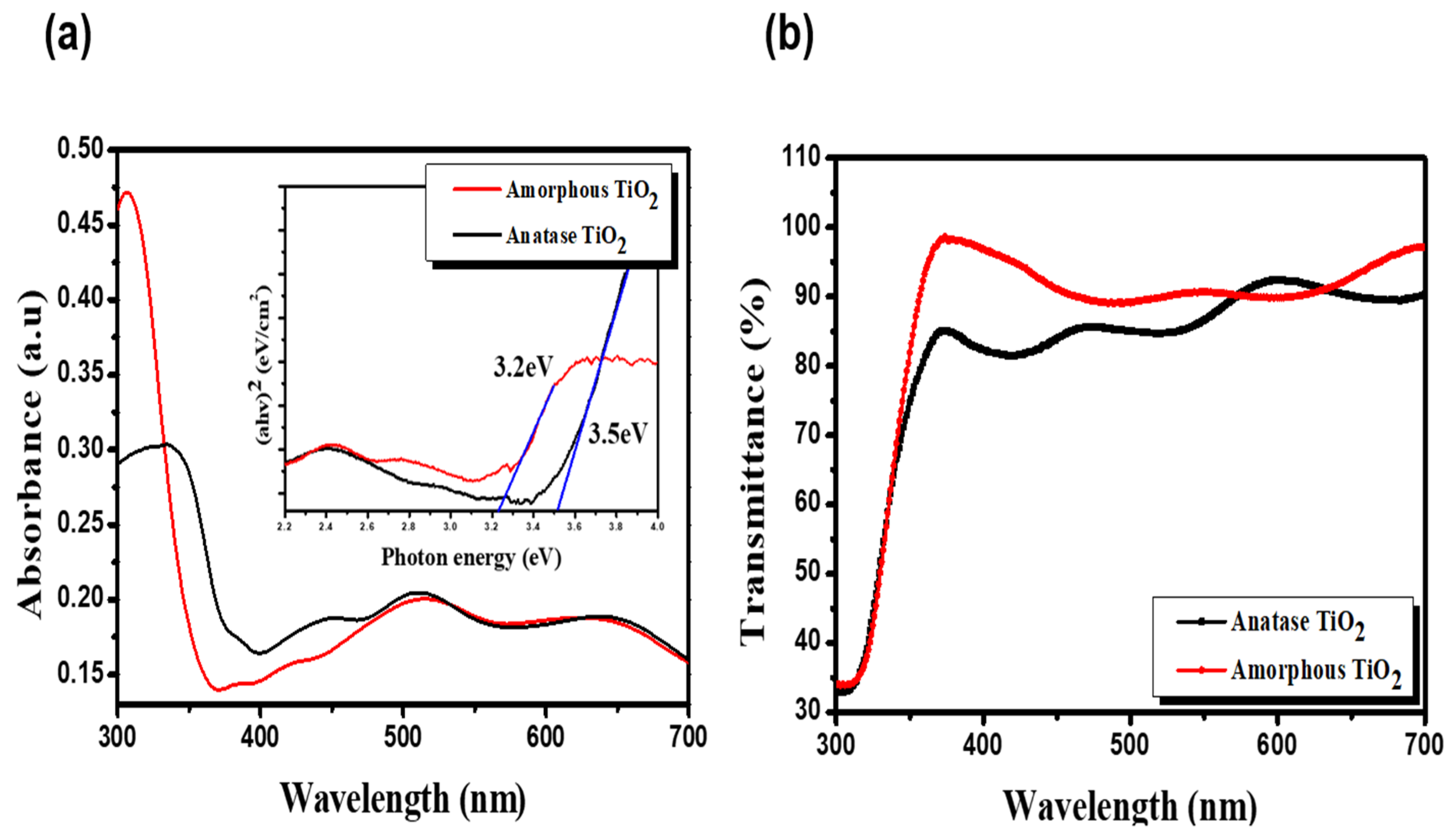
To investigate the optical properties of the Am- and An-TiO2 monolayers, the absorbance was measured using UV-vis spectroscopy. Figure 4a shows the absorbance spectra of the Am- (black line) and An- (red line) TiO2 NSs monolayers. It clearly shows that the Am- and An-TiO2 monolayers absorb only a range of UV light due to their wide band gap. We calculated the optical band gap of the used TiO2 monolayers from a Tauc plot, as displayed in the inset image of Figure 4a, by a plot of the (ahv)2 versus hv curves [30].
Here, A is a constant, hv is the incident photon energy, Eg is the optical band gap, α is an absorption coefficient, and the value of m is 1/2 for indirect transitions. The calculated band gaps for the Am- and An-TiO2 monolayers are about 3.5 eV and 3.2 eV, respectively. The bandgaps of fabricated TiO2 monolayers are very similar to previously reported values [31].
In addition, Figure 4b shows the transmittance spectra of the Am-TiO2 sphere and An-TiO2 sphere monolayers. The transmittances of the Am-TiO2 sphere and An-TiO2 sphere monolayers were, respectively, 91.1 and 83.9% at a 450 nm wavelength. The high transmittance of TiO2 spheres in the visible region resulting from their wide band gap and thickness of the monolayer indicates that TiO2 NSs monolayers can be used as a light extractor in visible LEDs.
3.3. Effects of TiO2 NS Monolyaer on the Device Performance of LED
Following experimental methods, we fabricated TiO2 NS arrays/LED chips. Figure S1a,b shows optical microscope images of a blue LED chip with Am- and An-TiO2 NSs. The images clearly show that the TiO2 NS monolayer was successfully formed and transferred on the fabricated LEDs chip via the icing transfer method. The magnified SEM images of Am- (Figure S1c,d) and An-TiO2 (Figure S1e,f) NS arrays formed on p-GaN show the well-aligned sphere arrays of Am- and An-TiO2 without surface damage.
The effects on the light extraction efficiency (LEE) of Am-TiO2 and An-TiO2 monolayers being transferred onto LED chips were investigated by optical and electrical performance measurements. The electroluminescence (EL) spectra for LED chips with Am- and An-TiO2 monolayers were measured at the fixed injection current of 20 mA, as shown in Figure 5a. The effect on EL intensity of LED chips with Am-TiO2 NS array is the strongest among the three samples. The integrated EL intensity of the samples covered with An-TiO2 NS and Am-TiO2 NS arrays exhibited enhancements of 1.3 and 7.9 times, respectively, over that of the reference LED chips at 443 nm emission wavelength. Optical microscopy images of emitted light obtained from LED chips with Am- and An-TiO2 monolayer arrays are shown in the inset of Figure 5a.
LED chip with Am-TiO2 monolayer arrays showed the brightest emission intensity and uniform emission area at a low current injection of 0.5 mA. These indicate that Am-TiO2 NS monolayers can dramatically improve the light extraction of LED chips. In addition, to evaluate the LEE of the LED chips, light output powers (LOPs) –current–voltage (L-I-V) were measured at the injection current ranging from 0 to 100 mA, as shown in Figure 5b. The LOPs of the Am-TiO2 NSs array/LEDs chip were higher by factors of 2.8 and 3.1 times compared to the An-TiO2 monolayer=coated LED chip and reference LED chip, respectively, at 100 mA. This large enhancement in the LOP of LED chips with Am-TiO2 NS arrays can be attributed to the efficient propagation of light from the GaN layer to the TiO2 NS and superior mitigation of back reflection of light at the interface of TiO2 NSs and air [32,33]. The external quantum efficiency (EQE) of the LED chips with and without a TiO2 NS array at the injection current range of 0–100 mA were measured, as shown in Figure 5c. Although there are efficiency drops in data as current levels increase, LED chips with Am-TiO2 NS arrays still showed higher EQE than other LED chips. EQE is expressed as EQE = IQE × LEE, where IQE is the internal quantum efficiency and LEE is the light extraction efficiency. The values of IQE of all blue LED chips are assumed to be the same since they have the same epitaxial structure. Therefore, the improvement of the EQE of the LED chips with the Am-TiO2 NS arrays results from the increased LEE of the LED chips at I = 100 mA. The measured EQE from the samples covered with An- and Am-TiO2 NS arrays exhibited enhancements of 1.1 and 3.1 times more than a bare LED chip, respectively, at 100 mA. The EQEs of LEDs with Am-TiO2 NS arrays exhibit a stable boost of 3 times over LEDs with An-TiO2 NS arrays over the entire range of injection currents applied in this experiment. To design an adequate TiO2 NS monolayer array on LEDs, various parameters should be considered, such as the refractive index, crystal structure, and the packing density of spheres. Among the considered parameters described here, we paid special attention to the effects of the crystal structure of the spheres on the LEE of LED chips. In order to theoretically evaluate LEEs of LEDs with respect to changes in the refractive indices of used spheres monolayers, which can be modified by changes in the crystal phases of TiO2, we used the 3-D FDTD simulation method.
Figure 6a–c shows the far-field intensity mapping of the reference LED and LED chip with An- and Am-TiO2 sphere monolayer arrays. It is apparent that emitted light was trapped in the inner LED chip due to TIR resulting from the abrupt change in the refractive index across p-GaN and air in the reference LED chip. However, the LED with An-TiO2 monolayer arrays shows that light was effectively diffused from the LED chip through the An-TiO2 NSs, as clearly shown in Figure 6b. Furthermore, the Am-TiO2 monolayer array can more effectively diffuse a significant amount of light from the LED through the NSs, as depicted in Figure 6c. Similar to far-field intensity, Figure S2a–c shows the cross-section profiles of the power field for reference LED and LED chips with An- and Am-TiO2 sphere monolayer arrays. It is clear from Figure S2a that emitted light was trapped in LEDs due to the abrupt change in the refractive index across p-GaN and air in the reference LED chips. However, the LEDs with An-TiO2 and Am-TiO2 NSs monolayer arrays demonstrate that light was effectively diffused from the LED chips through the NSs, as shown in Figure S2b and S2c, respectively. The enhancement of light extraction from LEDs with Am-TiO2 NSs arrays can be attributed to the increase in the escape probability of photons from the LED as observed by simulation results. In addition, in terms of the escape angle of light, light emission of LED mainly occurred between 10° and 20° as denoted by the red dotted line in Figure 6a–c. The Am-TiO2 monolayer array/LED shows the highest light-emission intensity and brightest area among all samples. In addition, by comparison of the integrated power field intensity for LEDs with different spheres of TiO2 monolayers, LED chips with An-TiO2 monolayers and Am-TiO2 monolayer arrays exhibited, respectively, 1.4 times and 1.76 times higher intensity than LED chips without any structures.
To further investigate the increased light extraction via Am-TiO2 NS monolayers as compared to An-TiO2 NSs, we captured the evolution of traveling waves showing light propagation with respect to changes in time, as shown in Figure 7. When we compared the light extraction via different Am- and An-TiO2 NSs, light propagation modes in Am-TiO2 NSs were more strongly concentrated on the apex than were those of An-TiO2 as denoted by yellow arrows in Figure 7j,d, respectively. The backscattering portions of light in An-TiO2 spheres remaining from escaping via the top of TiO2 spheres toward GaN are clearly larger than those of Am-TiO2 as denoted by the red arrow in Figure 7f,l, respectively. Therefore, more photons can effectively escape from the apex of Am-TiO2 NS concentrated by the convex lens-focusing effects and propagated via Am- TiO2 NSs to air from the LEDs. This result further proved that the Am-TiO2 NSs are more effective than An-TiO2 NSs at improving the LEE of LEDs.
4. Conclusions
We successfully formed uniform monolayer arrays of TiO2 NSs on LED chips via the icing transfer method. After the transfer of TiO2 monolayers with different crystal phases onto LED chips, enhancements in the light extraction of LEDs were observed. The LEDs covered with Am- and An-TiO2 NS monolayers showed 3.0- and 1.05-fold enhancement of LOP intensity, respectively, compared with the reference LEDs without the NSs at a fixed injection current of 100 mA. The experimentally measured results are entirely consistent with those of 3D-FDTD simulations, and the large enhancement in the optical output power can be attributed to the superior suppression of the TIR and backscattering between the GaN layer and air by Am-TiO2 NS arrays and the concentration of light on the apex of spheres within light propagation path. Based on our results, the transferrable uniform arrays of Am- and An-TiO2 NS monolayers will open a new path to improve the optical performance of various optoelectronic devices, such as solar cells, photodetectors, and LED chips.
Supplementary Materials
The following supporting information can be downloaded at: https://0-www-mdpi-com.brum.beds.ac.uk/article/10.3390/app13053042/s1, Figure S1: (a,b) Optical microscope image of the TiO2 nanosphere arrays on blue LED chip with Am- and An-TiO2 nanosphere. (c,d) and (e,f) show the SEM images of 500nm size Am- and An-TiO2 nanosphere arrays on p-GaN substrate, respectively; Figure S2: (a–c) FDTD simulation results of compares cross sections of the power field for general planar LED and LEDs with Anatase-, Amorphous-TiO2 sphere array (d,e) Anatase, Amorphous-TiO2 single sphere cross section image; Table S1: Summary of synthesized TiO2 nanospheres sizes according to amount of the injected DIW.
Author Contributions
Conceptualization, J.P. and D.K.; methodology, D.K.; software, U.J.; validation, N.K. and D.K.; formal analysis, W.H.; investigation, D.K. and U.J.; writing—original draft preparation, D.K. and J.P.; writing—review and editing, N.K. and J.P.; supervision, J.P.; project administration, J.P.; funding acquisition, J.P. All authors have read and agreed to the published version of the manuscript.
Funding
This work was supported by the National Research Foundation of Korea(NRF) grant funded by the Korea government (MSIT) (No. 2021R1A4A1052085).
Conflicts of Interest
The authors declare no conflict of interest.
References
- You, Y.; Tian, W.; Min, L.; Cao, F.; Deng, K.; Li, L. TiO2/WO3 Bilayer as Electron Transport Layer for Efficient Planar Perovskite Solar Cell with Efficiency Exceeding 20%. Adv. Mater. Interfaces 2020, 7, 1901406. [Google Scholar] [CrossRef]
- Zhang, B.; Yang, F.; Liu, H.; Yan, L.; Yang, W.; Xu, C.; Huang, S.; Li, Q.; Bao, W.; Liu, B.; et al. Assembling Graphene-Encapsulated Pd/TiO2 Nanosphere with Hierarchical Architecture for High-Performance Visible-Light-Assisted Methanol Electro-Oxidation Material. Ind. Eng. Chem. Res. 2019, 58, 19486–19494. [Google Scholar] [CrossRef]
- Yang, T.; Park, S.J.; Kim, T.G.; Shin, D.S.; Park, J. Ultraviolet photodetector using pn junction formed by transferrable hollow n-TiO2 nano-spheres monolayer. Opt. Express 2017, 25, 30843–30850. [Google Scholar] [CrossRef]
- Zhu, K.; Li, Q.; Xue, Z.; Yu, Q.; Liu, X.; Shan, Z.; Liu, K. Mesoporous TiO2 Spheres as Advanced Anodes for Low-Cost, Safe, and High-Areal-Capacity Lithium-Ion Full Batteries. ACS Appl. Nano Mater. 2020, 3, 1019–1027. [Google Scholar] [CrossRef]
- Song, D.; Cui, P.; Wang, T.; Xie, B.; Jiang, Y.; Li, M.; Mbebgue, J.M. Bunchy TiO2 hierarchical spheres with fast electron transport and large specific surface area for highly efficient dye-sensitized solar cells. Nano Energy 2016, 23, 122–128. [Google Scholar] [CrossRef]
- Wu, F.; Zhou, Z.; Hicks, A.L. Life Cycle Impact of Titanium Dioxide Nanoparticle Synthesis through Physical, Chemical, and Biological Routes. Environ. Sci. Technol. 2019, 53, 4078–4087. [Google Scholar] [CrossRef] [PubMed]
- Elseman, A.M.; Zaki, A.H.; Shalan, A.E.; Rashad, M.M.; Song, Q.L. TiO2 Nanotubes: An Advanced Electron Transport Material for Enhancing the Efficiency and Stability of Perovskite Solar Cells. Ind. Eng. Chem. Res. 2020, 59, 18549–18557. [Google Scholar] [CrossRef]
- Ton, N.N.T.; Dao, A.T.N.; Kato, K.; Ikenaga, T.; Trinh, D.X.; Taniike, T. One-pot synthesis of TiO2/graphene nanocomposites for excellent visible light photocatalysis based on chemical exfoliation method. Carbon 2018, 133, 109–117. [Google Scholar] [CrossRef]
- Luo, H.; Dimitrov, S.; Daboczi, M.; Kim, J.S.; Guo, Q.; Fang, Y.; Stoeckel, M.A.; Samorì, P.; Fenwick, O.; Sobrido, A.B.J.; et al. Nitrogen-Doped Carbon Dots/TiO2 Nanoparticle Composites for Photoelectrochemical Water Oxidation. ACS Appl. Nano Mater. 2020, 3, 3371–3381. [Google Scholar] [CrossRef]
- Wang, H.; Lu, J.; Liu, L.; Cui, W.; Liang, Y. Ultra-thin rGO nanosheet modified TiO2 nanotube arrays for boosted photoelectrochemical performance. Appl. Surf. Sci. 2020, 506, 144966. [Google Scholar] [CrossRef]
- Chen, S.; Zhou, Y.; Luo, H.; Tang, L.; Guo, R.; Zhang, D. Core-shell TiO2@HfO2 nanowire arrays with designable shell thicknesses for improved permittivity and energy density in polymer nanocomposites. Compos. Part A Appl. Sci. Manuf. 2020, 137, 1060122. [Google Scholar] [CrossRef]
- Zhao, T.; Qian, R.; Tang, Y.; Yang, J.; Dai, Y.; Lee, W.I.; Pan, J.H. Controllable Synthesis and Crystallization of Nanoporous TiO2 Deep-Submicrospheres and Nanospheres via an Organic Acid-Mediated Sol−Gel Process. Langmuir 2020, 36, 7447–7455. [Google Scholar] [CrossRef]
- Yang, T.; Shin, D.S.; Yu, J.; Ji, Y.; Kim, T.G.; Dayakar, T.; Park, J. Fabrication of n-TiO2 hollow spheres monolayer-based UV detectors with different-sized nanospheres. Semicond. Sci. Technol. 2018, 33, 125018. [Google Scholar] [CrossRef]
- Dong, G.; Xia, D.; Yang, Y.; Zhang, W.; Fan, R.; Sui, L.; Su, L.; Zhao, Y.; Yang, P.; Li, Y. In-situ passivation of TiO2 mesoporous scaffold with nano-sizedheteropolyacid for boosting the efficiency of the perovskite solar cells. Electrochim. Acta 2020, 332, 135427. [Google Scholar] [CrossRef]
- Leem, Y.C.; Seo, O.; Jo, Y.R.; Kim, J.H.; Chun, J.; Kim, B.J.; Noh, D.Y.; Lim, W.; Kim, Y.; Park, S.J. Titanium oxide nanotube arrays for high light extraction efficiency of GaN-based vertical light-emitting diodes. Nanoscale 2016, 8, 10138–10144. [Google Scholar] [CrossRef]
- Désières, Y.; Chen, D.Y.; Visser, D.; Schippers, C.; Anand, S. Strong light extraction enhancement using TiO2 nanoparticles-based microcone arrays embossed on III-Nitride light emitting diodes. Appl. Phys. Lett. 2018, 112, 231101. [Google Scholar] [CrossRef] [Green Version]
- Celik, E.; Negi, R.S.; Bastianello, M.; Boll, D.; Mazilkin, A.; Brezesinski, T.; Elm, M.T. Tailoring the protonic conductivity of porous yttria-stabilized zirconia thin films by surface modification. Phys. Chem. Chem. Phys. 2020, 22, 1519–11528. [Google Scholar] [CrossRef]
- Kenanakis, G.; Katsarakis, N. Chemically grown TiO2 on glass with superior photocatalytic properties. J. Environ. Chem. Eng. 2014, 2, 1748–1755. [Google Scholar] [CrossRef]
- Démarest, N.; Deubel, D.; Keromnès, J.C.; Vaudry, C.; Grasset, F.; Lefort, R.; Guilloux-Viry, M. Optimization of bandpass optical filters based on TiO2 nanolayers. Opt. Eng. 2015, 54, 015101. [Google Scholar] [CrossRef] [Green Version]
- Kim, T.G.; Park, S.J.; Kim, D.; Shin, D.S.; Park, J. Improvement of the Optical and Electrical Performance of GaN-Based Light-Emitting Diodes (LEDs) Using Transferrable ZnSnO3 (ZTO) Microsphere Monolayers. ACS Sustain. Chem. Eng. 2018, 6, 11547–11554. [Google Scholar] [CrossRef]
- Shin, D.S.; Kim, T.G.; Kim, D.; Kim, K.K.; Park, J. Light Extraction Enhancement of GaN-Based Light-Emitting Diodes Using Hollow Silica Nanospheres. J. Nanosci. Nanotech. 2017, 17, 4073–4077. [Google Scholar] [CrossRef]
- Jung, U.; Kim, S.; Kim, D.; Shin, D.S.; Xian, Z.; Park, J. Metal—Semiconductor—Metal UV Detectors Using Transferrable Amorphous and Crystalline Zinc-Tin-Oxide Microsphere Monolayers. ACS Sustainable Chem. Eng. 2020, 8, 60–70. [Google Scholar] [CrossRef]
- Lu, Z.; Hanif, A.; Lu, C.; Sun, G.; Cheng, Y.; Li, Z. Thermal, mechanical, and surface properties of poly(vinyl alcohol) (PVA) polymer modified cementitious composites for sustainable development. J. Appl. Polym. Sci. 2018, 1, 46177. [Google Scholar] [CrossRef]
- Kim, D.; Song, K.M.; Jung, U.; Kim, S.; Shin, D.S.; Park, J. Effects of Different InGaN/GaN Electron Emission Layers/Interlayers on Performance of a UV-A LED. Appl. Sci. 2020, 10, 1514. [Google Scholar] [CrossRef] [Green Version]
- Ji, Y.; Jung, U.; Xian, Z.; Kim, D.; Yu, J.; Park, J. Ultraviolet photodetectors using hollow p-CuO nanospheres/n-ZnO nanorods with a pn junction structure. Sens. Actuator A Phys. 2020, 304, 111876. [Google Scholar] [CrossRef]
- Wei, Y.; Zhu, J.; Gan, Y.; Cheng, G. Titanium glycolate-derived TiO2 nanomaterials: Synthesis and applications. Adv. Powder Technol. 2018, 29, 2289–2311. [Google Scholar] [CrossRef]
- Zhao, T.; Qian, R.; Zhou, G.; Wang, Y.; Lee, W.I.; Pan, J.H. Mesoporous WO3/TiO2 spheres with tailored surface properties for concurrent solar photocatalysis and membrane filtration. Chemosphere 2021, 263, 128344. [Google Scholar] [CrossRef]
- Karimi Estahbanati, M.R.; Feilizadeh, M.; Shokrollahi Yancheshmeh, M.; Iliuta, M.C. Effects of Carbon Nanotube and Carbon Sphere Templates in TiO2 Composites for Photocatalytic Hydrogen Production. Ind. Eng. Chem. Res. 2019, 58, 2770–2783. [Google Scholar] [CrossRef]
- Su, D.; Dou, S.; Wang, G. Anatase TiO2: Better Anode Material Than Amorphous and Rutile Phases of TiO2 for Na-Ion Batteries. Chem. Mater. 2015, 27, 6022–6029. [Google Scholar] [CrossRef]
- Alamelu, K.; Ali, B.J. Sunlight driven photocatalytic performance of a Pt nanoparticle decorated sulfonated graphene–TiO2 nanocomposite. New J. Chem. 2020, 44, 7501–7516. [Google Scholar] [CrossRef]
- Scirè, D.; Macaluso, R.; Mosca, M.; Casaletto, M.P.; Isabella, O.; Zeman, M.; Crupi, I. Density of states characterization of TiO2 films deposited by pulsed laser deposition for heterojunction solar cells. Nano Res. 2022, 5, 4048–4057. [Google Scholar] [CrossRef]
- Leung, S.F.; Zhang, Q.; Xiu, F.; Yu, D.; Ho, J.C.; Li, D.; Fan, Z. Light Management with Nanostructures for Optoelectronic Devices. J. Phys. Chem. Lett. 2014, 5, 1479–1495. [Google Scholar] [CrossRef] [PubMed]
- Al-Amri, A.M.; Fu, P.H.; Lai, K.Y.; Wang, H.P.; Li, L.J.; He, J.H. Efficiency Enhancement of InGaN-Based Solar Cells via Stacking Layers of Light-Harvesting Nanospheres. Sci. Rep. 2016, 6, 28671. [Google Scholar] [CrossRef] [PubMed] [Green Version]
Figure 1.
Process flow from formation of TiO2 monolayer to its transfer on LED chips. (a) Formation of TiO2 NSs ML on a PDMS, (b) drop-casting of DI water and flip of TiO2/PDMS pad, (c) removing of PDMS from TiO2 NSs ML, (d) formation of arrays of TiO2 NSs ML on LED chips.
Figure 1.
Process flow from formation of TiO2 monolayer to its transfer on LED chips. (a) Formation of TiO2 NSs ML on a PDMS, (b) drop-casting of DI water and flip of TiO2/PDMS pad, (c) removing of PDMS from TiO2 NSs ML, (d) formation of arrays of TiO2 NSs ML on LED chips.

Figure 2.
SEM images of (a) Am- and (b) An-TiO2 NSs. The inset figure shows the size distributions of used TiO2 NSs.
Figure 2.
SEM images of (a) Am- and (b) An-TiO2 NSs. The inset figure shows the size distributions of used TiO2 NSs.

Figure 3.
(a) XRD patterns of as-synthesized and thermally annealed TiO2 NSs and HR-TEM images and SAED patterns of (b) anatase and (c) amorphous spheres.
Figure 3.
(a) XRD patterns of as-synthesized and thermally annealed TiO2 NSs and HR-TEM images and SAED patterns of (b) anatase and (c) amorphous spheres.

Figure 4.
(a) Absorbance spectra and (b) transmittance of TiO2 monolayers using An- (dot-line) and Am-TiO2 (black-line) nanosphere monolayers.
Figure 4.
(a) Absorbance spectra and (b) transmittance of TiO2 monolayers using An- (dot-line) and Am-TiO2 (black-line) nanosphere monolayers.

Figure 5.
(a) EL spectra of LED chips with An- and Am-TiO2 NS arrays with an injection current of 20 mA. Emission images of LED chips are shown in inset. (b) L-I-V curves and (c) external quantum efficiency (EQE) of LED chips with different TiO2 NS arrays as a function of injected current (at I = 0~100 mA).

Figure 6.
Far-field intensity mappings of (a) a reference LED and LEDs with (b) An-TiO2 and (c) Am-TiO2 NS monolayers.
Figure 6.
Far-field intensity mappings of (a) a reference LED and LEDs with (b) An-TiO2 and (c) Am-TiO2 NS monolayers.

Figure 7.
Evolution of travelling light via An-TiO2 NSs (a–f) and Am-TiO2 NSs (g–l) with respect to change of time. The red arrows represent the backscattering from the interface of air/TiO2 sphere to p-GaN.
Figure 7.
Evolution of travelling light via An-TiO2 NSs (a–f) and Am-TiO2 NSs (g–l) with respect to change of time. The red arrows represent the backscattering from the interface of air/TiO2 sphere to p-GaN.

Disclaimer/Publisher’s Note: The statements, opinions and data contained in all publications are solely those of the individual author(s) and contributor(s) and not of MDPI and/or the editor(s). MDPI and/or the editor(s) disclaim responsibility for any injury to people or property resulting from any ideas, methods, instructions or products referred to in the content. |
© 2023 by the authors. Licensee MDPI, Basel, Switzerland. This article is an open access article distributed under the terms and conditions of the Creative Commons Attribution (CC BY) license (https://creativecommons.org/licenses/by/4.0/).
Share and Cite
MDPI and ACS Style
Kim, D.; Jung, U.; Heo, W.; Kumar, N.; Park, J. Arrays of TiO2 Nanosphere Monolayers on GaN-Based LEDs for the Improvement of Light Extraction. Appl. Sci. 2023, 13, 3042. https://0-doi-org.brum.beds.ac.uk/10.3390/app13053042
AMA Style
Kim D, Jung U, Heo W, Kumar N, Park J. Arrays of TiO2 Nanosphere Monolayers on GaN-Based LEDs for the Improvement of Light Extraction. Applied Sciences. 2023; 13(5):3042. https://0-doi-org.brum.beds.ac.uk/10.3390/app13053042
Chicago/Turabian StyleKim, Dohyun, UiJin Jung, Wonjun Heo, Navneet Kumar, and Jinsub Park. 2023. "Arrays of TiO2 Nanosphere Monolayers on GaN-Based LEDs for the Improvement of Light Extraction" Applied Sciences 13, no. 5: 3042. https://0-doi-org.brum.beds.ac.uk/10.3390/app13053042
Note that from the first issue of 2016, this journal uses article numbers instead of page numbers. See further details here.