Dispersion of the Retardation of a Photoelastic Modulator


1
School of Data Science and Technology, North University of China, Taiyuan 030051, China
2
Engineering and Technology Research Center of Shanxi Province for Opto-Electric Information and Instrument, Taiyuan 030051, China
3
School of Optical and Electronic Information, Huazhong University of Science and Technology, Wuhan 430074, China
4
School of Electrical and Control Engineering, North University of China, Taiyuan 030051, China
*
Author to whom correspondence should be addressed.
Appl. Sci. 2019, 9(2), 341; https://0-doi-org.brum.beds.ac.uk/10.3390/app9020341
Submission received: 11 December 2018
/
Revised: 26 December 2018
/
Accepted: 9 January 2019
/
Published: 19 January 2019
(This article belongs to the Section Optics and Lasers)
Abstract
:Recently, ellipsometry and polarization imaging using photoelastic modulators (PEMs) have been applied to a wide spectral range, from vacuum ultraviolet to the mid-infrared wavelengths. To ensure high accuracy polarization performance, the accurate calibration of the retardation of PEM is crucial. In this report, the dispersion of the retardation of the PEM is studied. According to the operational principle of PEM, their retardation can be separated into independent dispersion and driving terms. The effect attributed to the dispersion on PEM retardation calibration is experimentally explored. These experiments indicate that the dispersion term can be defined in advance using the refractive index of the photoelastic crystal under incident light, and that the driving term is directly proportional to the amplitude of the driving voltage. The calibration method for the retardation amplitude of the PEM, which considers dispersion, is also demonstrated. The results show that the relative deviation between the calibration and actual measurement values of PEM retardation amplitude are less than 1%. This study presents an accurate way to calibrate the PEM retardation and supports the application of PEMs in a wide range of wavelengths.
1. Introduction
A photoelastic modulator (PEM) is a dynamic retarder with variable retardation based on the photoelastic effect [1,2], whereby the piezoelectric actuator excites and maintains the mechanical vibration in the photoelastic crystal when a sinusoidal driving voltage is applied, which typically forms a stress standing wave and results in a periodic variation of birefringence in the photoelastic crystal, and thus the phase and polarization states of the incident light are modulated by the temporal modulation birefringence. The PEM retarder is similar to a waveplate with a fixed retardation axis and sinusoidally varying retardation values. Compared to the other polarization modulators, such as Faraday rotator, electro-optic modulator, and liquid crystal variable retarder, PEMs have a high modulation frequency, a high modulation purity and efficiency, good retardation stability and a large acceptance angle and aperture, which provides accurate and flexible modulation of the polarization state of the incident light over a wide range of wavelengths, from vacuum ultraviolet (UV) (~l20 nm) to mid-infrared (mid-IR) (~16 μm) [3]. Since their introduction, PEMs have been successfully applied to optical rotation measurements, circular dichroism measurements, ellipsometry, polarization imaging, etc. [4,5,6,7,8].
To ensure the highly accurate polarization performance of the PEM, the user is required to accurately calibrate its retardation. Recently, ellipsometry and polarization imaging using PEM have been applied to a wide spectral range, from the vacuum visible to the mid-IR wavelengths [7,9,10]. Due to the dispersion of the retardation of the PEM, its accurate calibration at a number of wavelengths is a complex problem. In 1999, Theodore C. Oakberg concluded that voltages applied on the half-wave retardation amplitudes of the PEM were a variable in the wavelengths, which revealed the dispersion phenomenon of the PEM [11]. Until now, there has been no detailed PEM calibration method considering the differences induced by different wavelengths of the incident light, which has been reported. For single wavelength light, the observation oscilloscope waveform and the application of Bessel functions are the two typical PEM calibration methods [12]. The oscilloscope waveform observation method can be used to calibrate the PEM retardation amplitude of a half-wave or radians, when a flattop waveform is observed on the oscilloscope. For the method using Bessel function zeros, the retardation amplitudes of the PEM are set to 2.405, 3.872 and 5.136 rad, respectively, when the zeroth, first, and second Bessel functions are zero, and the corresponding harmonic components are nulled. The two methods can only calibrate the PEM retardation for the special values mentioned above. The method that uses the ratio of multiple-harmonic components is developed to calibrate large numbers of retardation amplitudes of the PEM [13,14]. The calibration of the PEM retardation at any amplitude for incident light with different wavelengths combined with this method is a promising area for further investigation.
In this report, based on the fundamental principle of photoelastic modulation, we present the principle analysis of the dispersion of the PEM and experimentally explore the effect attributed to the dispersion on the calibration of the PEM retardation. Furthermore, we also demonstrate an optimized calibration method for the PEM retardation, which considers the dispersion.
2. Principle Analysis of the Dispersion of the PEM
The photoelastic modulation effect is a type of artificial birefringence phenomenon, the discovery of which has led to the development of a series of optical modulation devices. The most commonly used PEMs are the two-dimensional symmetric shape PEMs with large aperture and low static residual birefringence, using a piezoelectric actuator mounted on a photoelastic crystal. Typically, a −18.5° X-cut quartz crystal plate is chosen as the piezoelectric actuator, and there are several types of isotropic materials, such as fused silica, CaF2, ZnSe, and monocrystalline silicon, which can be used as the photoelastic crystal, enabling the extension of the spectral range from UV to terahertz. The structures and vibration forms of the PEMs are shown in Figure 1.
The frequency of the length stretching vibration of the piezoelectric actuator matches with the natural frequency of the vibration of the photoelastic crystal. Based on the inverse piezoelectric effect, the mechanical vibration in the photoelastic crystal is excited and maintained by the piezoelectric actuator, which typically forms a stress standing wave and results in a periodic variation of the birefringence, while the phase and polarization states of the incident light are modulated by the variable birefringence. When a sinusoidal voltage (, where is the voltage amplitude and is the resonant frequency) is applied to the piezoelectric actuator, the stress standing wave in the photoelastic crystal can be expressed as [15]
where L is the length of the photoelastic crystal, and spatial variables x and y extend from −L/2 to L/2. The amplitude of the stress, , is proportional to the and can simply be defined as , is a coefficient related to the inverse piezoelectric effect of the actuator and the mount between the actuator and the photoelastic crystal, and is the phase delay between the vibration in the photoelastic crystal and the driving voltage. Further, the stress induced by the birefringence in the photoelastic crystal can be expressed as
where is the refractive index of the isotropic material, while and are the photoelastic constants. When the light beam propagates in the PEM along with the z-axis, the phase and polarization states of the incident light are periodically modulated along the x and y-axes by the variable birefringence. The modulation retardation of the PEM can be described as
where is the wavelength of the incident light, and is the thickness of the photoelastic crystal. According to the Equations (1) and (2), Equation (3) can be rewritten as
Thus, we can define the retardation of the PEM as , and the amplitude of the PEM retardation can be further written as using the method of the separation of variables, where is defined as , which can be attributed to the dispersion of the PEM retardation. Therefore, is denoted as the dispersion term, and , which is proportional to the applied voltage amplitude and defined as , is denoted as the driving term. Here, the simplification coefficient , representing the driving efficiency of the PEM, can be considered as a summary of the characteristics of the PEM, such as geometric features, the inverse piezoelectric effect of the actuator, the photoelastic effect of the crystal, and the mount between the actuator and the photoelastic crystal. Although the values of are slightly different for individual PEMs, they can be accurately calibrated after the PEM is manufactured and the location of the incident light beam is established. Thus, the retardation of PEM can be simplified as
3. Experiment
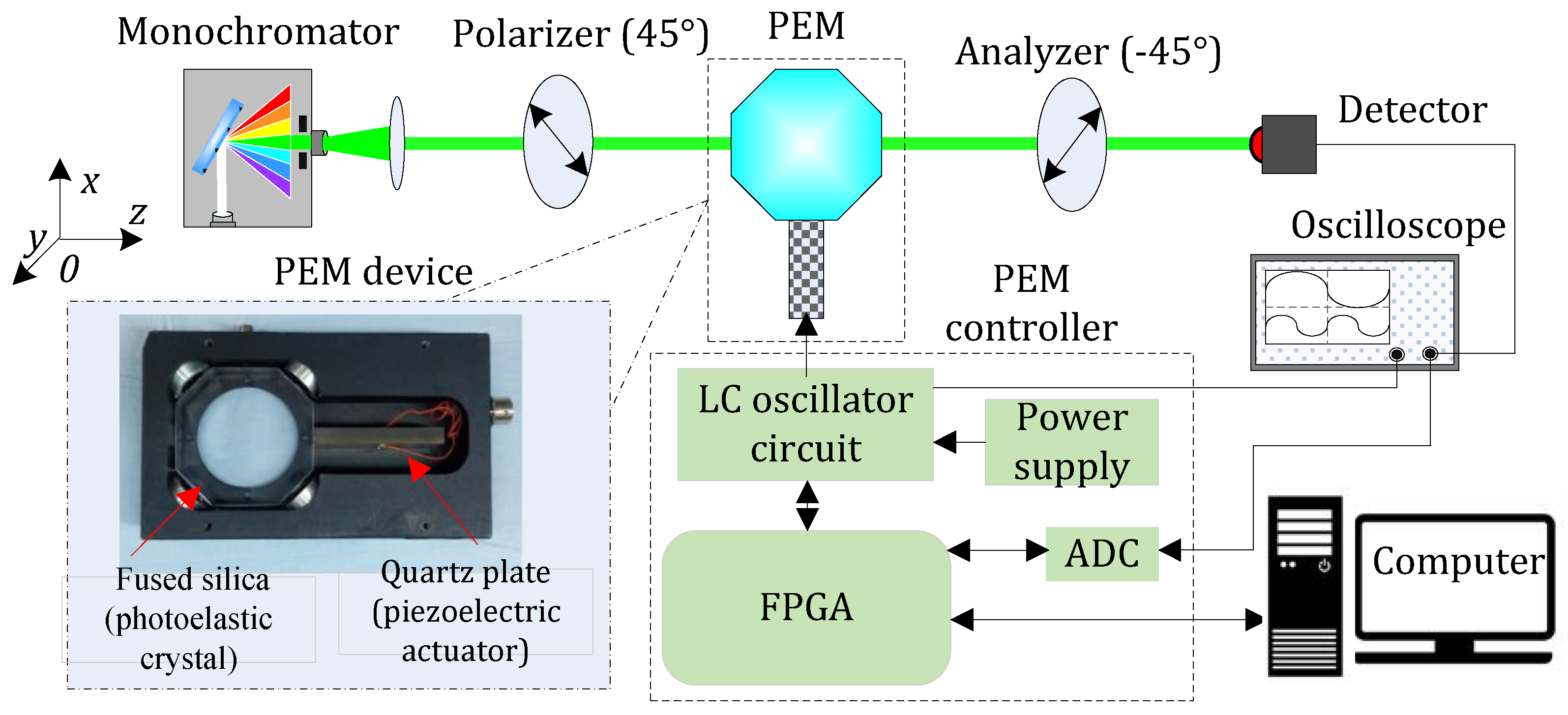
In order to study the dispersion of the retardation of the PEM and obtain an accurate calibration method for the PEM retardation, a fused silica PEM was employed, which was widely applied at the visible light range using fused silica as the photoelastic crystal. The fused silica PEM was custom made by our research group, while the photoelastic crystal was a regular octagon fused silica disk with an edge length of 22.50 mm and a thickness of 16.00 mm. The mounted piezoelectric actuator was an −18.5° x-cut quartz plate with a size of 6.48 mm × 51.08 mm × 19.18 mm. A field programmable gate array (FPGA) provided square wave signals, and an LC oscillator circuit transformed the square wave signals to sinusoidal high voltage for the operation of the PEM. The frequency and amplitude of the sinusoidal driving voltage could be regulated by the FPGA and a power supply, respectively. The FPGA, the LC oscillator circuit, and the power supply constitute the PEM controller while the optical head comprises the fused silica disk and the quartz plate. The experimental system for the measurement and calibration of the PEM retardation is illustrated in Figure 2.
A xenon lamp monochromator (Omni-λ 200, Zolix Instruments Co., Ltd., Beijing, China), in the light range of 400–800 nm, with a spectral band less than 1 nm, was used as the light source. The light source was collimated to pass through a polarizer, the center of the fused silica PEM, and an analyzer to be detected by a Si photodetector (FPDA510-FC, Thorlabs China, Shanghai, China). Both the polarizer and analyzer were Glan-Taylor polarizers with an extinction ratio greater than 100,000:1, and the transmission axes of the polarizer and the analyzer were orthogonal in an arrangement of 45° and −45°, respectively. The modulation fast axis of the PEM was set to 0°. According to the polarization analysis [16], the light intensity arriving at the photodetector can be expressed as
where is the total intensity of the incident light. The retardation can be further expanded using Bessel function of the first kind, and Equation (6) can be rewritten as
where is the zeroth order of the Bessel function, k is a positive integer, and is the (2k)th order of the Bessel function. An Altera EP3C FPGA is used to provide the PEM driving signal, to maintain a fast and precise 12-bit analog-to-digital converter clock frequency, and then to complete the digital signal processing [17,18]. Multiple even harmonic components such as the second, the forth harmonics can be achieved as
The multiple harmonic components are directly proportional to the light intensity and the Bessel function. By using the ratio of multiple harmonic components, the retardation amplitude of the PEM can be calibrated by
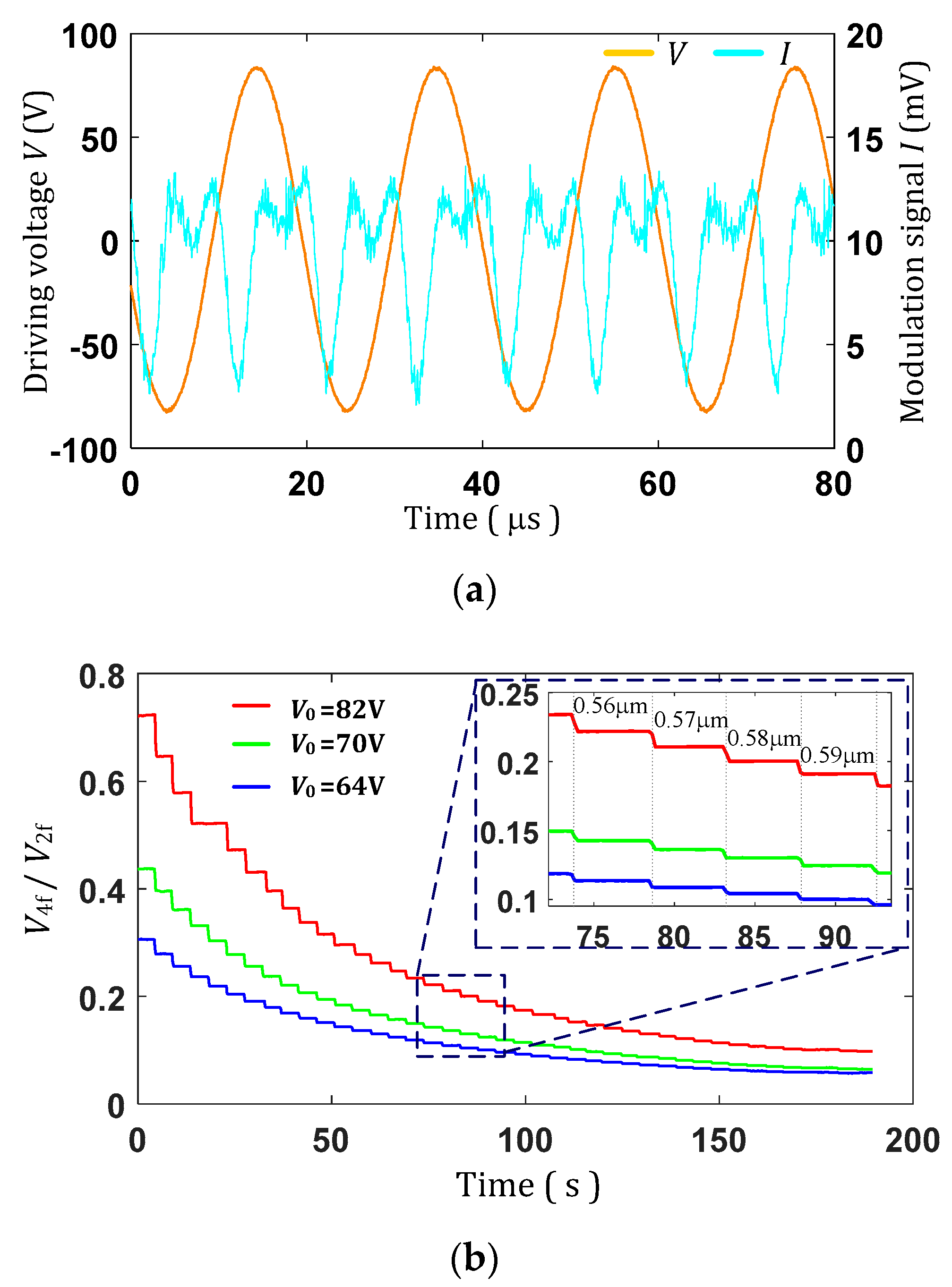
The influence of the intensity fluctuation of the light source can be effectively eliminated, and this calibration method is insensitive to the misalignment of the polarizer and analyzer transmission axes. The amplitudes of the driving voltage were set to 82 V, 70 V and 64 V, respectively. The driving voltage and the modulation signals are shown in Figure 3a, and the ratio of the second and forth harmonic components are shown in Figure 3b,c.
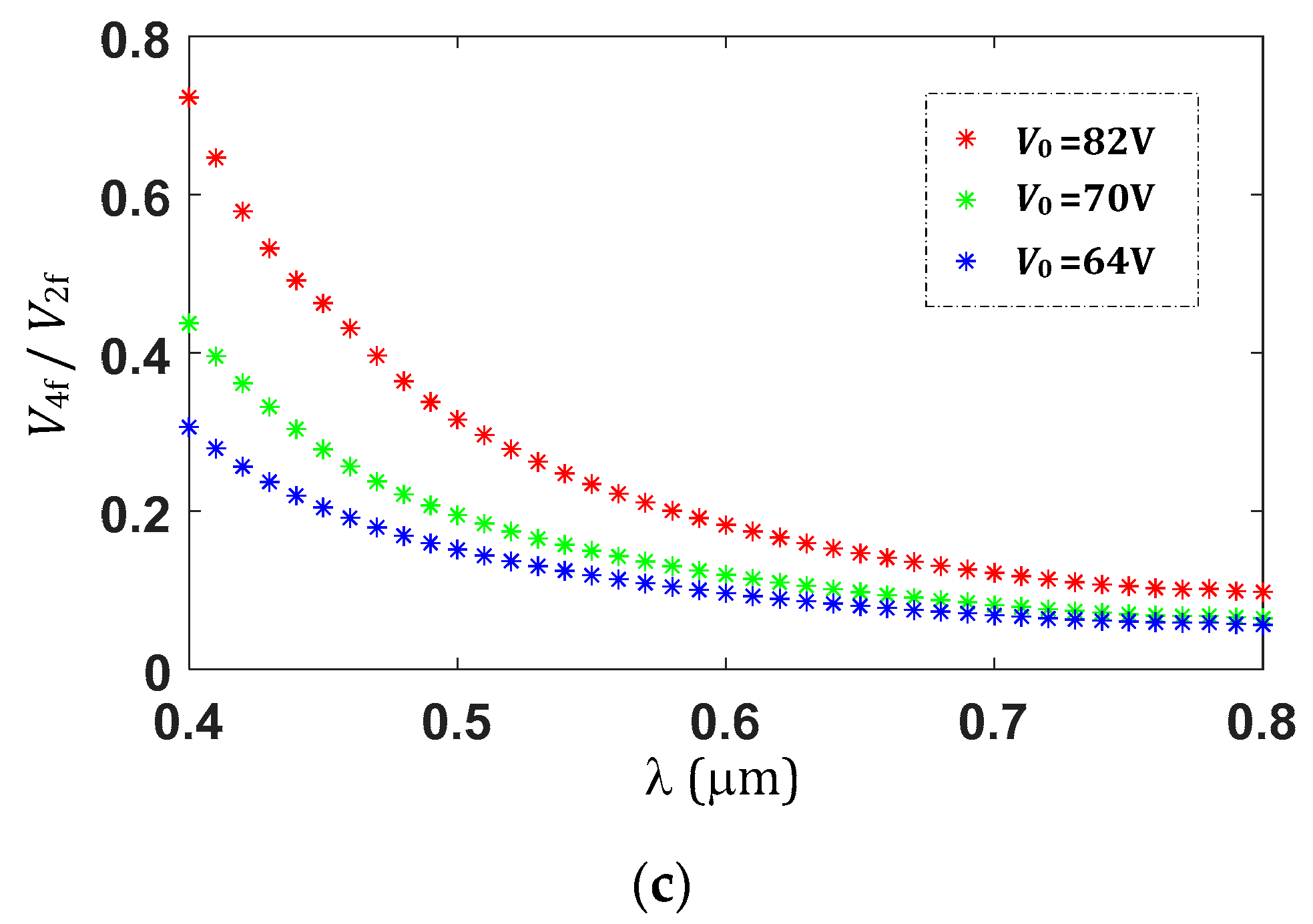
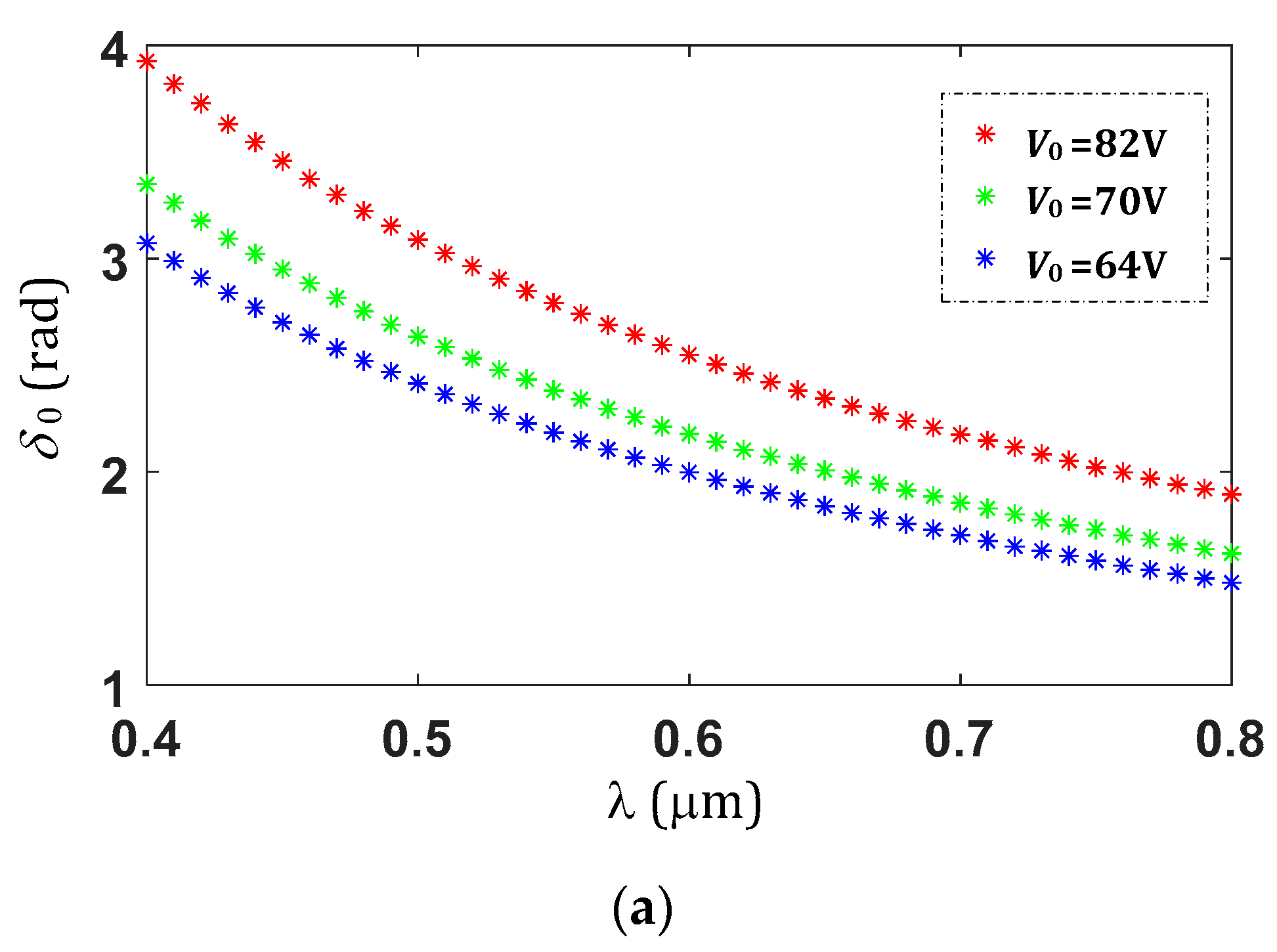
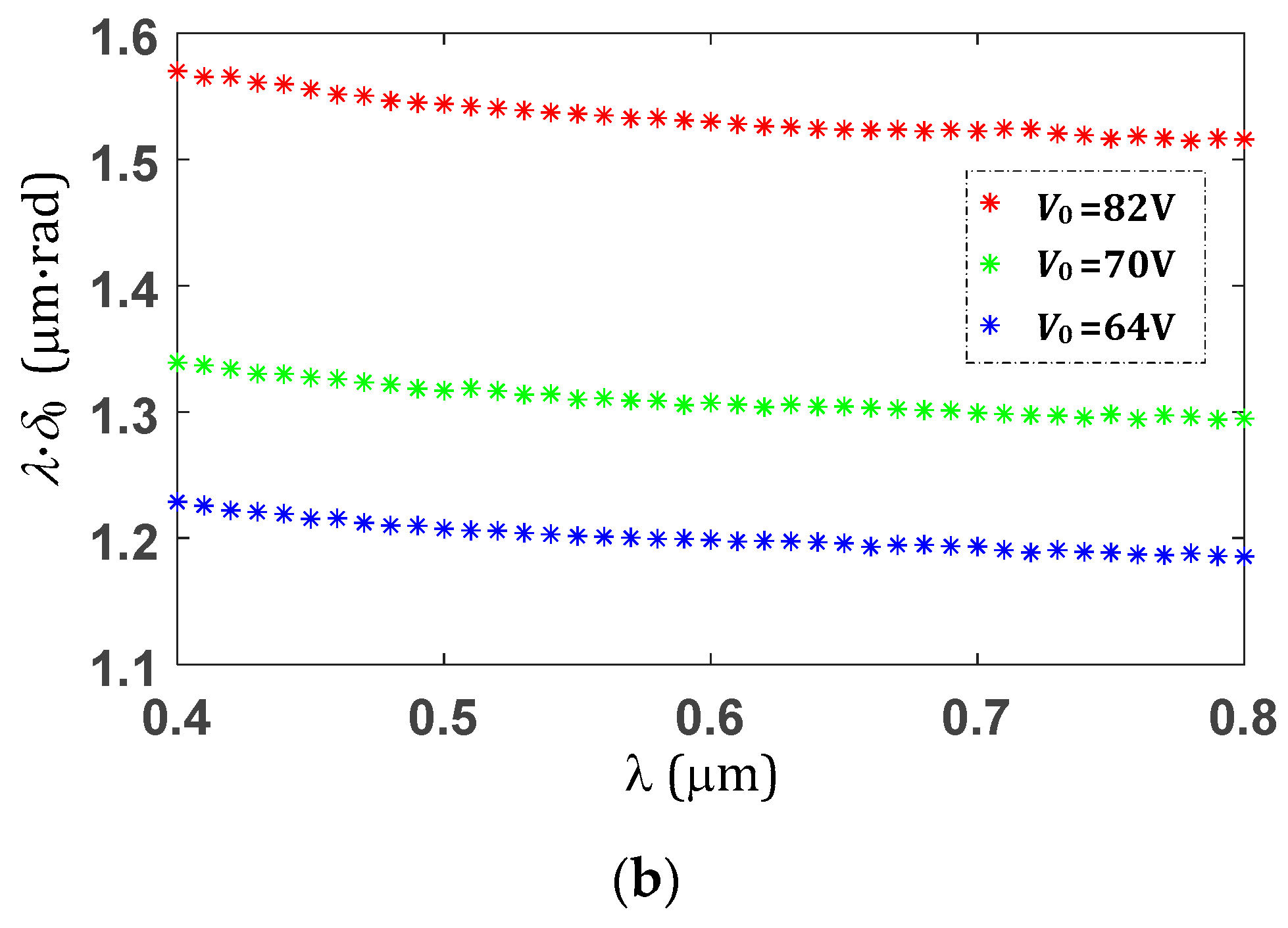
The modulation signal in Figure 3a was acquired by the FPGA and the harmonic components obtained by use of the digital phase-locked technique. The ratio of the second and forth harmonic components in the experiment was obtained. As can be seen in Figure 3b,c, the ratio decreases with the increase in the wavelength, and it is directly proportional with the driving voltage at the same light wavelength. Combing Equation (8) and the Bessel function, the ratios shown in Figure 3b,c can be used to calibrate the retardation amplitude of the PEM; the calibration results are shown in Figure 4a. The retardation amplitude also decreases with the increase in the wavelength and shows a noticeable dispersion. To eliminate the difference in the values due to the wavelength, we also observed the retardance (), as shown in Figure 4b.
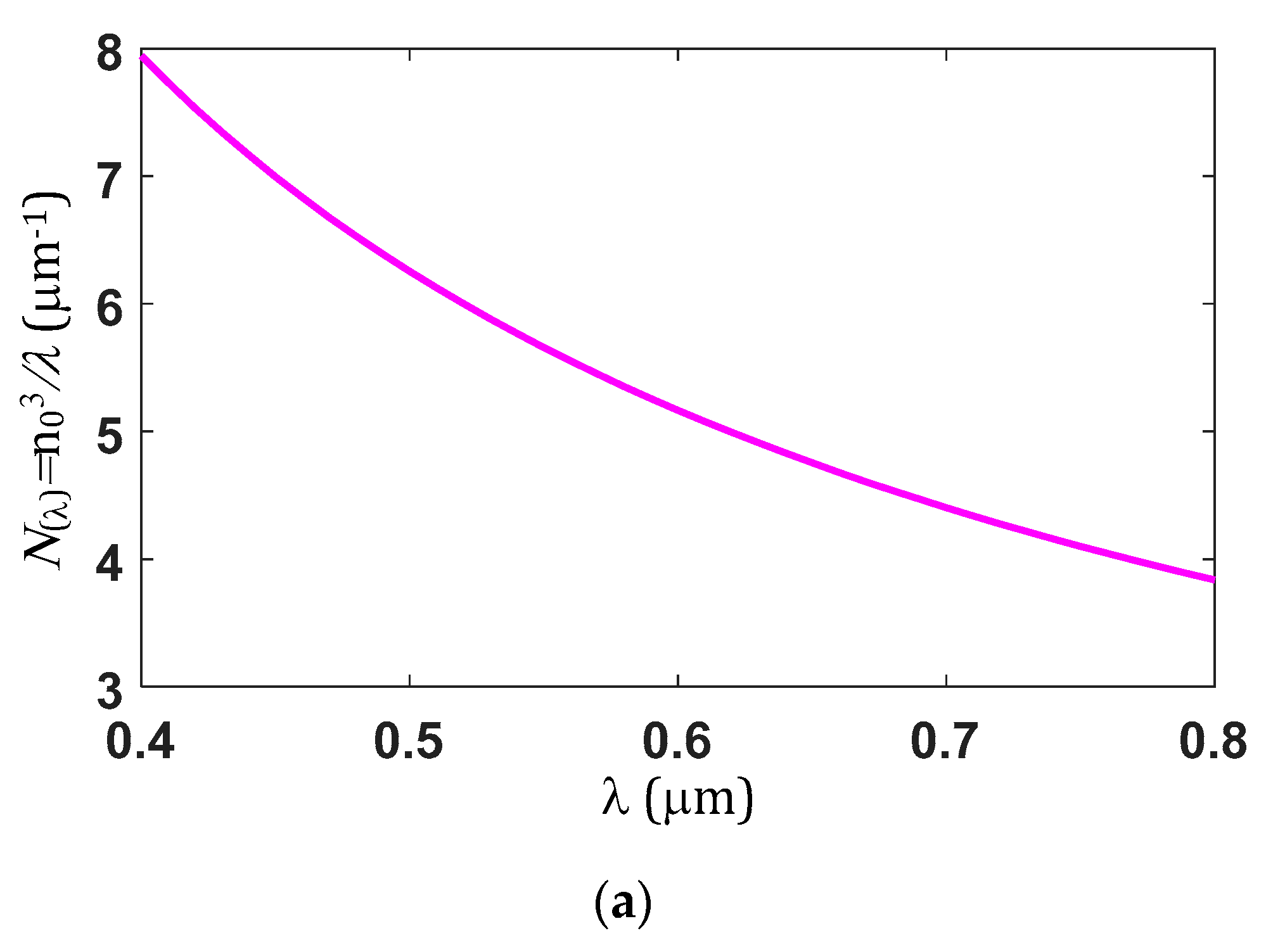
As can be seen in Figure 4b, the PEM retardance also decreases slightly with the increase in the wavelength and shows a dispersion characteristic. According to the theoretical analysis concluded in Equation (5), it is suggested that the retardance dispersion is introduced by the dispersion of the fused silica photoelastic crystal. According to Reference [19], the dispersion of the refractive index of the fused silica can be described by the Sellmeier equation as
thus, the dispersion terms in Equation (5) are obtained in the wavelength range of 0.4–0.8 μm, as shown in Figure 5a.
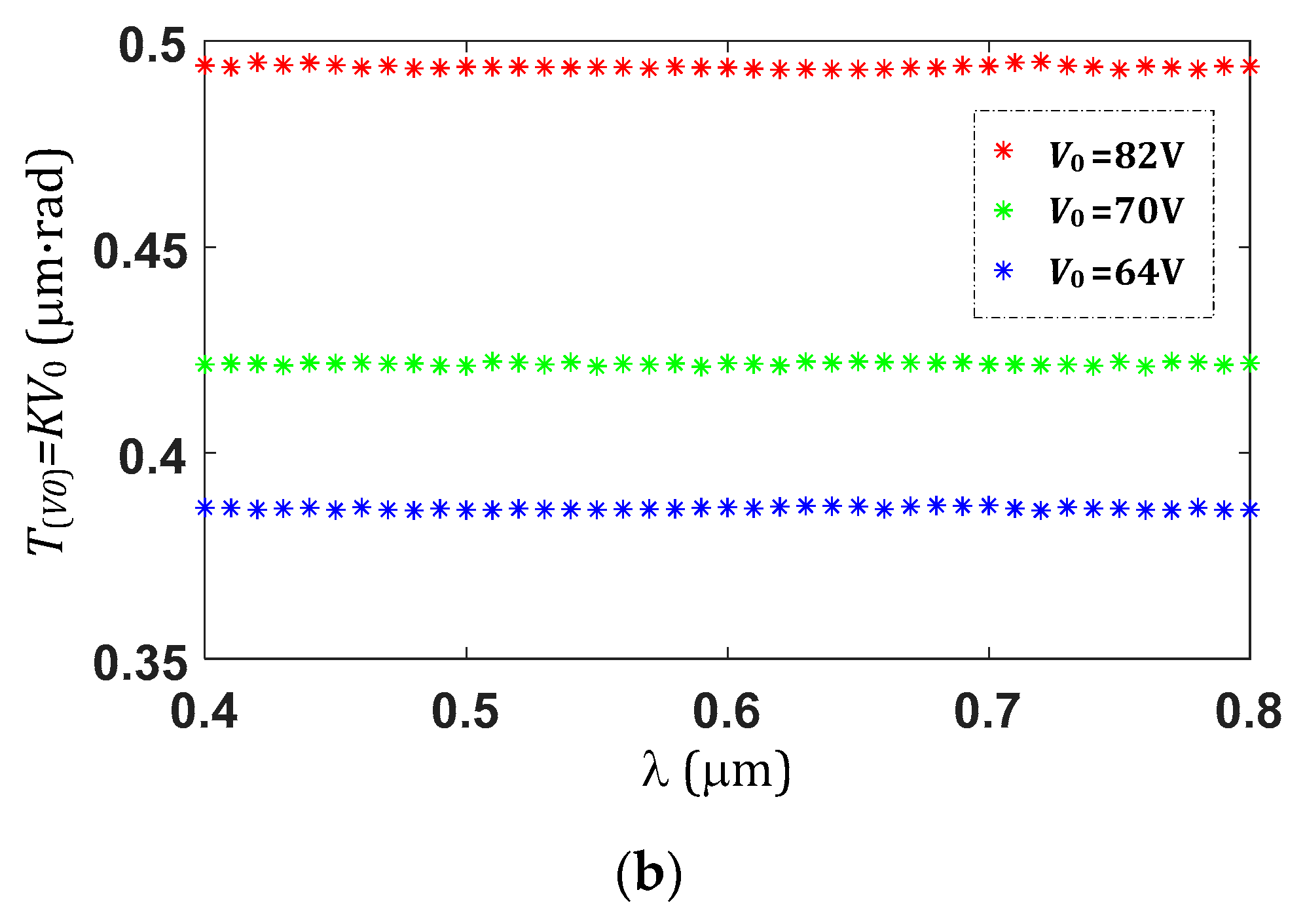
By using the retardation amplitude of the PEM, shown in Figure 4b, and the dispersion term, shown in Figure 5a, the driving term was determined at different driving voltages. As can be seen in Figure 5b, the driving term, as a function of the incident light wavelength, is nearly constant. The mean value and standard deviation of the driving term is also determined and summarized in Table 1.
4. Discussion
A calibration method for the retardation amplitude of the PEM in a wide wavelength range, which considers the dispersion, can be easily found. The calibration method can be determined as follows: (i) First, the calibration of the dispersion term, can be defined by using the Sellmeier equation describing the refractive index of the photoelastic crystal under the incident light wavelength, as illustrated in Figure 5a; (ii) then, the driving term, can be calibrated by obtaining the retardation amplitudes of the PEM at different driving voltages applied on a single wavelength incident light.
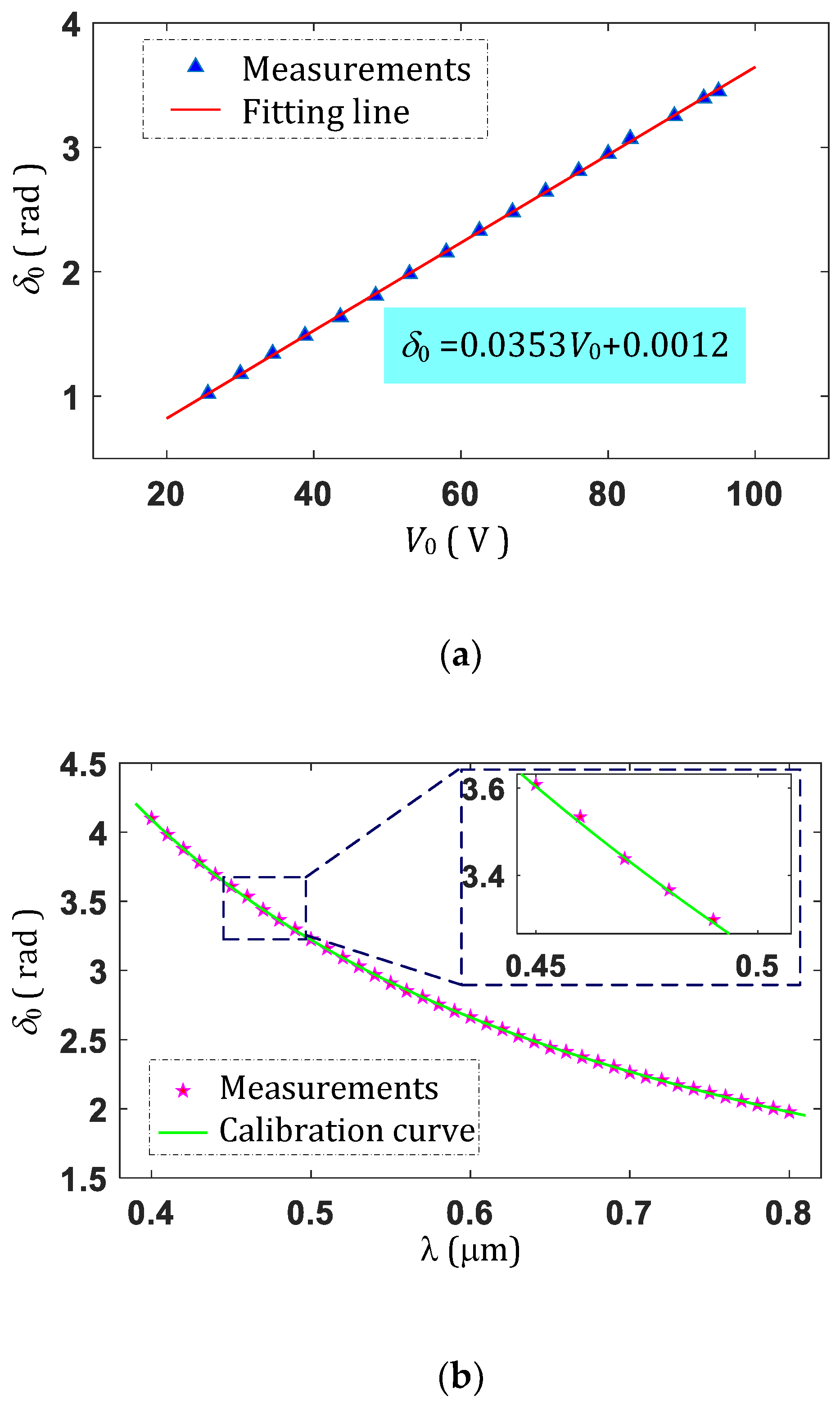
To further verify the validity and maneuverability of the calibration method, the monochromator was replaced by a diode laser at center wavelength of 532 nm as the incident light source. We varied the driving voltage of the PEM from 25.6 V to 95 V, and obtained the PEM retardation amplitudes, as shown in Figure 6a. The PEM retardation shows a good linear relationship with the driving voltage. The equation of the fitting line is ; therefore, the driving efficiency coefficient can be accurately calibrated using Equation (5), where the slope of the fitting line corresponds to the driving efficiency coefficient . Then, the amplitudes of the PEM retardation can be calibrated for different incident light wavelengths at different driving voltages, by combining the dispersion term and the driving efficiency coefficient. The driving voltage was set to 85.5 V, and the calibration curve of the amplitudes of the PEM retardation was determined by substituting the dispersion term, the driving efficiency coefficient , and the driving voltage . The calibration curve is shown in Figure 6b. The light source was changed back to the monochromator, the PEM retardation amplitudes were also measured for the incident light wavelength in the range of 0.4–0.8 μm, and the actual measurement values are also recorded in Figure 6b.
As can be seen in Figure 6b, the actual measured values of are in agreement with the calibration values. The calibration results show that the deviation between the calibration values and the measurement values, , is maximal when the wavelength of the incident light is 0.46 μm. The maximal deviation that corresponds to the relative deviation is , which indicates the calibration method for the PEM retardation is accurate.
5. Conclusions
In summary, experimental studies have been carried out on the dispersion of the retardation amplitude of a PEM. The retardation amplitude can be separated into independent dispersion and driving terms. Specifically, the dispersion of the retardation of the PEM is due to the dispersion term, resulting from the difference in the incident light wavelengths and the dispersion of the refractive index of the photoelastic crystal. Therefore, the dispersion item can be defined in advance by using the Sellmeier equation, which describes the refractive index of the photoelastic crystal under incident light. The driving term is directly proportional to the amplitude of the driving voltage, and the driving efficiency coefficient can be accurately calibrated for different driving voltages under a single wavelength incident light. The calibration of the retardation amplitude of the PEM, which considers the dispersion at a wide range of wavelengths, was demonstrated. The relative deviation between the measurement and calibration results was less than 1%. The study in this report can be used as a suitable reference for the accurate retardation calibration of PEM applications at a wide range of wavelengths.
Author Contributions
S.W. and K.L. developed the theory; S.W., X.H. and K.L. conceived and designed the experiments; S.W. and Y.W. performed the experiments; X.H. and K.L. analyzed the data; S.W. and K.L. wrote the paper.
Funding
This research was funded by Ministry of Science and Technology of the People’s Republic of China, grant number 2013DFR10150, National Natural Science Foundation of China, grant numbers 61505179, 61505180.
Acknowledgments
The authors are grateful to Zhibin Wang for fruitful discussions.
Conflicts of Interest
The authors declare no conflict of interest.
References
- Wang, B.; List, J. Basic optical properties of the photoelastic modulator: Part I. Useful aperture and acceptance angle. SPIE Proc. 2005, 58881, 58881I. [Google Scholar]
- Li, K.W.; Wang, Z.B.; Wang, L.M.; Zhang, R. 45° double-drive photoelastic modulation. J. Opt. Soc. Am. A 2016, 33, 2041. [Google Scholar]
- Brown, J.M.; Smullin, S.J.; Kornack, T.W.; Romalis, M.V. New Limit on Lorentz-and C P T-Violating Neutron Spin Interactions. Phys. Rev. Lett. 2010, 105, 151604. [Google Scholar] [CrossRef] [PubMed]
- Satozono, H. Elimination of artifacts derived from the residual birefringence of a phase modulator for circular dichroism by retardation domain analysis. Opt. Lett. 2015, 40, 1161–1164. [Google Scholar] [CrossRef] [PubMed]
- Maccaferri, N.; Berger, A.; Bonetti, S.; Bonanni, V.; Kataja, M.; Qin, Q.H. Tuning the magneto-optical response of nanosize ferromagnetic Ni disks using the phase of localized plasmons. Phys. Rev. Lett. 2013, 111, 167401. [Google Scholar] [CrossRef] [PubMed]
- Garcia-Caurel, E.; De Martino, A.; Gaston, J.P.; Yan, L. Application of spectroscopic ellipsometry and Mueller ellipsometry to optical characterization. Appl. Spectrosc. 2013, 67, 1–21. [Google Scholar] [CrossRef] [PubMed]
- Maccaferri, N.; Gregorczyk, K.; De Oliveira, T.V.; Kataja, M.; Van Dijken, S.; Pirzadeh, Z.; Vavassori, P. Ultrasensitive and label-free molecular level detection enabled by light phase control in magnetoplasmonic nanoantennas. Nat. Commun. 2015, 6, 6150. [Google Scholar] [CrossRef] [PubMed]
- Diner, D.J.; Xu, F.; Martonchik, J.V.; Rheingans, B.E.; Geier, S.; Jovanovic, V.M.; Davis, A.; Chipman, R.A.; McClain, S.C. Exploration of a Polarized Surface Bidirectional Reflectance Model Using the Ground-Based Multiangle SpectroPolarimetric Imager. Atmosphere 2012, 3, 591–619. [Google Scholar] [CrossRef] [Green Version]
- Alali, S.; Gribble, A.; Vitkin, I.A. Rapid wide-field Mueller matrix polarimetry imaging based on four photoelastic modulators with no moving parts. Opt. Lett. 2016, 41, 1038–1041. [Google Scholar] [CrossRef] [PubMed]
- Jian, H.; Shi, H.; Sun, X.; Gao, B. Optical Anisotropy of Few-Layer Black Phosphorus Visualized by Scanning Polarization Modulation Microscopy. ACS Photonics 2018, 5, 2509. [Google Scholar] [CrossRef]
- Oakberg, T.C. Calibration of photoelastic modulators in the vacuum uv. SPIE Proc. 2000, 4133, 101–112. [Google Scholar]
- Zeng, A.; Huang, L.; Dong, Z.; Hu, J.; Huang, H.; Wang, X. Calibration method for a photoelastic modulator with a peak retardation of less than a half-wavelength. Appl. Opt. 2007, 46, 699–703. [Google Scholar] [CrossRef] [PubMed]
- Wang, M.W.; Tsai, F.H.; Chao, Y. In situ calibration technique for photoelastic modulator in ellipsometry. Thin Solid Films 2004, 455, 78–83. [Google Scholar] [CrossRef]
- Wang, M.W.; Chao, Y.F.; Leou, K.C.; Tsai, F.H.; Lin, T.L.; Chen, S.S.; Liu, Y.W. Calibrations of phase modulation amplitude of photoelastic modulator. Jpn. J. Appl. Phys. 2004, 43, 827. [Google Scholar] [CrossRef]
- Diner, D.J.; Davis, A.; Hancock, B.; Gutt, G.; Cairns, R.A.; Chipman, B. Dual photoelastic modulator based polarimetric imaging concept for aerosol remote sensing. Appl. Opt. 2007, 46, 8428–8445. [Google Scholar] [CrossRef] [PubMed]
- Liu, Y.W.; Jones, G.A.; Peng, Y.; Shen, T.H. Generalized theory and application of Stokes parameter measurements made with a single photoelastic modulator. J. Appl. Phys. 2006, 100, 063537. [Google Scholar] [CrossRef] [Green Version]
- Li, K.W.; Zhang, R.; Ning, J.; Cheng, Y.H.; Zhang, M.J.; Wang, L.M.; Wang, Z.B. Fast and full range measurements of ellipsometric parameters using a 45°dual-drive symmetric photoelastic modulator. Opt. Express 2017, 25, 5725–5733. [Google Scholar]
- Li, K.; Wang, S.; Wang, L.; Yu, H.; Jing, N.; Xue, R.; Wang, Z. Fast and Sensitive Ellipsometry-Based Biosensing. Sensors 2018, 18, 15. [Google Scholar] [CrossRef] [PubMed]
- Malitson, I.H. Interspecimen comparison of the refractive index of fused silica. J. Opt. Soc. Am. 2013, 55, 1205–1209. [Google Scholar] [CrossRef]
Figure 1.
Schematic diagram of two-dimensional symmetric photoelastic modulators (PEMs) with stretching and contraction vibrations.
Figure 1.
Schematic diagram of two-dimensional symmetric photoelastic modulators (PEMs) with stretching and contraction vibrations.

Figure 2.
Schematic diagram of the experimental system. The inset shows a PEM device.

Figure 3.
Modulation signals and the ratio of multiple harmonic components. (a) Waveform as shown on the oscilloscope at λ = 0.4 μm; channel V represents the driving voltage signal, with a peak driving voltage of 164 V (with amplitude of V0 = 82 V), and channel I is the modulation signal, with a peak value of 13.2 mV; (b) ratio of the second and forth harmonic components in the experiment, where the wavelength of the incident light was increased by 10 nm increments for about 4.5 s, from 0.4 μm to 0.8 μm; (c) mean value of the ratio of the second and forth components varied in the wavelength range of 0.4–0.8 μm, obtained by the averaging of the ratios shown in (b) for every light wavelength.


Figure 4.
(a) Amplitude of the PEM retardation and (b) PEM retardance.


Figure 5.
(a) Dispersion term and (b) driving term .


Figure 6.
Calibration and measurement of , (a) vs. , at a wavelength of 0.532 μm; (b) vs. , the inset shows a magnification of the vs. curve.
Figure 6.
Calibration and measurement of , (a) vs. , at a wavelength of 0.532 μm; (b) vs. , the inset shows a magnification of the vs. curve.


Table 1.
Mean value and standard deviation of the driving term.
| Driving Voltage (V) | Driving Term (μm⋅rad) | |
|---|---|---|
| Mean Value | Standard Deviation | |
| 64 | 0.38654 | 3.6 × 10⁻⁴ |
| 70 | 0.42166 | 3.6 × 10⁻⁴ |
| 82 | 0.49376 | 4.0 × 10⁻⁴ |
© 2019 by the authors. Licensee MDPI, Basel, Switzerland. This article is an open access article distributed under the terms and conditions of the Creative Commons Attribution (CC BY) license (http://creativecommons.org/licenses/by/4.0/).
Share and Cite
MDPI and ACS Style
Wang, S.; Han, X.; Wang, Y.; Li, K. Dispersion of the Retardation of a Photoelastic Modulator. Appl. Sci. 2019, 9, 341. https://0-doi-org.brum.beds.ac.uk/10.3390/app9020341
AMA Style
Wang S, Han X, Wang Y, Li K. Dispersion of the Retardation of a Photoelastic Modulator. Applied Sciences. 2019; 9(2):341. https://0-doi-org.brum.beds.ac.uk/10.3390/app9020341
Chicago/Turabian StyleWang, Shuang, Xie Han, Yaning Wang, and Kewu Li. 2019. "Dispersion of the Retardation of a Photoelastic Modulator" Applied Sciences 9, no. 2: 341. https://0-doi-org.brum.beds.ac.uk/10.3390/app9020341
Note that from the first issue of 2016, this journal uses article numbers instead of page numbers. See further details here.