GaN-based Vertical-Cavity Surface-Emitting Lasers Incorporating Dielectric Distributed Bragg Reflectors
by
Tatsushi Hamaguchi
, 
Hiroshi Nakajima
and
Noriyuki Fuutagawa
Compound Semiconductor Development Department, Application Technology Development Division, Sony Corporation, Atsugi, Kanagawa 243-0014, Japan
Appl. Sci. 2019, 9(4), 733; https://0-doi-org.brum.beds.ac.uk/10.3390/app9040733
Submission received: 22 January 2019
/
Revised: 14 February 2019
/
Accepted: 18 February 2019
/
Published: 20 February 2019
(This article belongs to the Special Issue Group III-V Nitride Semiconductor Microcavities and Microemitters)
Abstract
:This paper reviews past research and the current state-of-the-art concerning gallium nitride-based vertical-cavity surface-emitting lasers (GaN-VCSELs) incorporating distributed Bragg reflectors (DBRs). This paper reviews structures developed during the early stages of research into these devices, covering both major categories of GaN-based VCSELs: hybrid-DBR and all-dielectric-DBR. Although both types exhibited satisfactory performance during continuous-wave (CW) operation in conjunction with current injection as early as 2008, GaN-VCSELs have not yet been mass produced for several reasons. These include the difficulty in controlling the thicknesses of nitride semiconductor layers in hybrid-DBR type devices and issues related to the cavity dimensions in all-dielectric-DBR units. Two novel all-dielectric GaN-based VCSEL concepts based on different structures are examined herein. In one, the device incorporates dielectric DBRs at both ends of the cavity, with one DBR embedded in n-type GaN grown using the epitaxial lateral overgrowth technique. The other concept incorporates a curved mirror fabricated on (000-1) GaN. Both designs are intended to mitigate challenges regarding industrial-scale processing that are related to the difficulty in controlling the cavity length, which have thus far prevented practical applications of all-dielectric GaN-based VCSELs.
1. Introduction
For more than two decades, gallium nitride (GaN) has attracted interest with regard to applications in a wide range of optical devices, such as light-emitting diodes (LEDs) and laser diodes (LDs) [1,2]. Recently, GaN-based vertical-cavity surface-emitting lasers (VCSELs) have received considerable attention as a result of their superior characteristics, including low threshold currents, array formation capability, applicability to high-frequency operation, low manufacturing costs and high efficiencies [3,4,5,6,7,8,9,10,11,12,13]. Due to these advantages, GaN-based VCSELs have the potential to replace conventional LEDs and edge emitting LDs as light sources for optical storage, laser printers, projectors, displays, solid state lighting, optical communications, biosensors and many other applications.
This review summarizes recent progress in the development of GaN-based VCSELs. In the former sections, an overview of GaAs-based VCSELs is initially provided, followed by a discussion of hybrid DBR GaN-based VCSELs, in which the DBRs are made of semiconductors and dielectric materials. In the latter sections, all-dielectric-DBR VCSELs reported in the early stage of research into such devices are examined, after which the latest progress in other types of all-dielectric-DBR VCSELs based on epitaxial lateral overgrowth [14,15] and curved mirrors [16,17] is summarized.
2. GaAs-based VCSELs
Gallium-arsenide (GaAs) materials possess properties that are conducive to VCSEL lasing. These materials can be used to fabricate high-reflectivity mirrors and it is thus possible to obtain highly reflective DBRs using arsenide semiconductors via epitaxial growth techniques [18]. One common approach to fabricating GaAs-based VCSELs is to employ AlGaAs materials having two different compositions [19]. Varying the composition of AlGaAs leads to negligible changes in its lattice constant, so that AlGaAs DBR pairs can be grown in large numbers, which is required to achieve a reflectance close to 100%. In addition, GaAs-based materials provide a suitable means of establishing current paths in VCSELs, since AlGaAs DBRs are conductive in both p- and n-type layers. Therefore, a metallic electrode deposited on the outside of each DBR can provide a path for current injection into active regions located between p- and n-type layers. In addition, a layer of an arsenide such as AlAs placed next to the active layers is readily oxidized, thus allowing lateral confinement of the current [20]. The resulting structures give devices capable of concentrating carriers within the limited physical space defined by the active layers so as to enhance population inversion, which is essential for lasing. The third advantage of GaAs-based VCSELs is that a short cavity length can be readily obtained by epitaxial growth. All layers, including both DBRs, p-type and n-type layers and quantum wells, can be grown directly on a GaAs substrate using an epitaxial growth technique such as metal organic chemical vapor deposition (MOCVD).
3. Hybrid-DBR GaN-based VCSELs
These approaches do not necessarily work well when fabricating GaN-based VCSELs. The major researching interest in this case is the formation of nitride semiconductor DBRs for n-side mirrors. Lu et al. reported the first demonstration of continuous wave lasing from a GaN-VCSEL, in which the n-side DBR comprised 29 AlN/GaN bilayers grown directly on a GaN substrate by MOCVD [4,5]. In this device, a half-wavelength AlN stack was inserted between every four pairs of AlN/GaN quarter-wavelength stacks to produce the DBR. These AlN stacks suppressed the formation of cracks potentially resulting from the lattice mismatch between GaN and AlN.
In contrast, other groups have reported a DBR made of AlInN and GaN. Doping AlN with In reduces the lattice mismatch with GaN to zero [6,7], so this approach is expected to produce crack-free layers. The incorporation of this DBR structure into GaN-based VCSELs has been intensively investigated, primarily by a group at Meijo University [3,7,21] and a significant volume of data regarding threshold current, efficiency and optical output has been reported. This type of GaN-VCSEL has recently demonstrated a remarkably high output power above 10 mW together with a peak wall plug efficiency of 8.9% by Stanley Electronics [22].
However, the small refractive index difference between the two layers is problematic because a large number of layers is required to obtain high reflectivity. It has also been reported that the AlInN growth rate is so low that 12 h are required to grow a DBR with 40 AlInN/GaN DBRs bilayers [7]. The narrow stopband width of epitaxially grown n-side DBRs is another concern with regard to eventual mass production. The lasing wavelength of a VCSEL should ideally be located on the plateaus at which both DBRs exhibit high reflectance, meaning that the lasing mode makes use of the small mirror loss observed upon lasing. However, variations in the fabrication process could disrupt this set of conditions. As an example, a change in the thickness of the DBR layers would shift the position of the stopband. The stopband width for AlGaN/GaN bi-layers is reported to be 19 nm above 90% [7]. Thus, a change in the thickness of a DBR layer having a reflective center at 450 nm by only a small percentage, which is likely to occur in mass production, will shift the reflectance peak by approximately 10 nm. This shift would be sufficient to displace the stopband from the precisely-designed lasing wavelength. Therefore, there will likely be challenges associated with any future mass production of hybrid-DBR GaN-based VCSELs.
4. All-dielectric-DBR GaN-based VCSELs
In addition to nitride semiconductors, it may be possible to fabricate DBR mirrors having wide stopbands with dielectric materials, due to the wide range of refractive indices of these substances. As an example, the two dielectric materials SiO2 and Ta2O5 exhibit a large refractive index difference. Assuming refractive index values of 1.5 and 2.0 for the two dielectric materials and a reflectance peak wavelength of 450 nm, the associated stopband width would be more than 80 nm, which is much wider than the values reported for nitride semiconductor DBRs. Thus, GaN-based VCSELs with dielectric DBRs could avoid some of the issues associated with nitride semiconductor DBRs.
In a pragmatic approach reported by Higuchi et al., both DBRs were made of dielectric materials [8], adopting a p-side structure similar to that of Lu et al. [4,5]. The p-side was bonded to a silicon wafer while the n-side was polished to generate a thin nitride plate so as to obtain p-type, active and n-type layers on the silicon wafer. Subsequently, a dielectric DBR acting as the n-side mirrors and other metallic electrodes were deposited. In this process, both mirrors were composed of crack-free dielectric materials possessing wide stopbands. To date, there have been numerous reports of work with this type of GaN-based VCSEL [8,9,10,11,12,13].
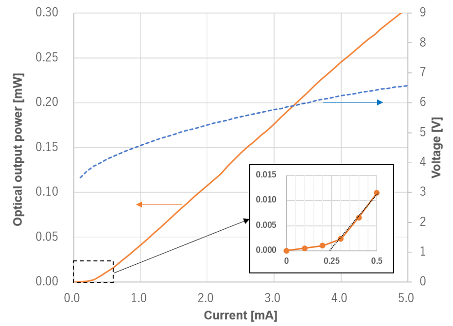
These GaN-VCSEL devices still have associated difficulties regarding control of the cavity length. Typically, the cavity must simultaneously meet two conditions to allow laser operation. The first condition concerns the optical mode loss and Figure 1a,b plot the roughly estimated coupling (diffraction) loss and mode spacing as functions of cavity length [16]. Figure 1a demonstrates that a shorter cavity is preferable because it leads to a smaller coupling (diffraction) loss after a round trip. Accounting for an estimated gain of up to 2000 cm−1 [23], the amplification resulting from the active layer in the VCSEL is estimated to be approximately 1% for a typical total thickness on the order of 10 nm. Thus, the cavity should preferably be shorter than several microns to limit the diffraction loss to less than 1%. The second condition concerns the longitudinal modes. The wavelength of each longitudinal mode is determined from the cavity length, which must be controlled so that one of the modes overlaps with the gain spectrum of the active region used in the device. As an example, even though the loss in such devices appears to be sufficiently low, in the case of a 5-μm-long cavity, the mode spacing is approximately 7 nm (Figure 1b). Consequently, the modes can easily miss the gain spectrum and lasing will not occur unless the cavity length is precisely controlled such that one of the longitudinal modes is located near the top of the gain spectrum of the InGaN quantum wells. It is evident that highly sophisticated technology would be required to control the cavity length to below several microns by polishing. Longer cavities can provide narrower longitudinal mode spacing to ensure that one of the modes appears near the top of the gain spectrum without precise control of the cavity length. For example, a cavity longer than 20 μm gives rise to a longitudinal mode spacing narrower than 2 nm, which is sufficiently narrow to overlap the gain spectrum of typical InGaN quantum wells. However, a cavity of this length often results in a diffraction loss of greater than 1%, which is sufficient to prevent the device from lasing. These requirements for precise control over the cavity length have thus far prevented the mass production of GaN-VCSELs.
It is apparent that precise control over the cavity length (to below 5 μm) or reduction of the optical diffraction associated with longer cavities, is required for the robust production of GaN-based VCSELs with all-dielectric DBR configurations. As an alternative to the approach reported by Higuchi et al., in which a lapping process is used to provide a basal plane for dielectric DBR deposition, a thinning technique based on photoelectrochemical (PEC) etching [24] was found to result in an operable GaN-VCSEL with a short cavity of 1.2 μm. If this approach allows precise control of cavity length, it could enable mass production of GaN-VCSELs. However, there has thus far only been limited research into this technique and further work is required to ensure that precise cavity length control is possible, as demonstrated by stability of the lasing wavelength over a wafer.
5. All-dielectric-DBR GaN-based VCSELs Fabricated by Epitaxial Lateral Overgrowth
To mitigate some of the challenges associated with existing all-dielectric-DBR GaN-based VCSELs, the present author’s group developed a GaN-based VCSEL with a novel structure [14,15,25]. This device incorporated dielectric DBRs at both ends of the cavity, with the DBR on one side embedded in n-type gallium nitride grown by the epitaxial lateral overgrowth (ELO) technique [26]. This type of GaN-based VCSEL has several advantages, including the ability to form highly reflective dielectric DBR mirrors at both ends of the cavity and precise control of short cavity lengths during the epitaxial growth process.
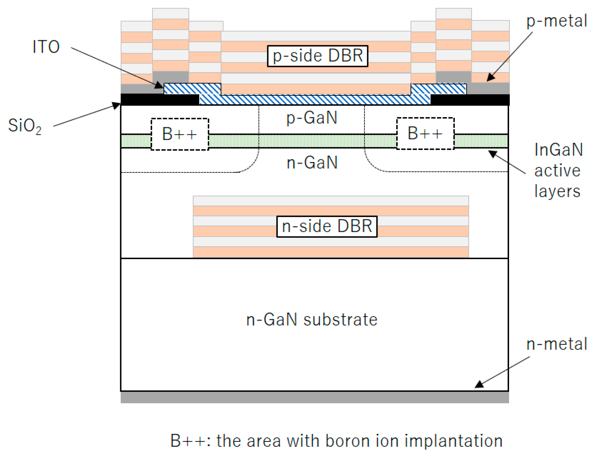
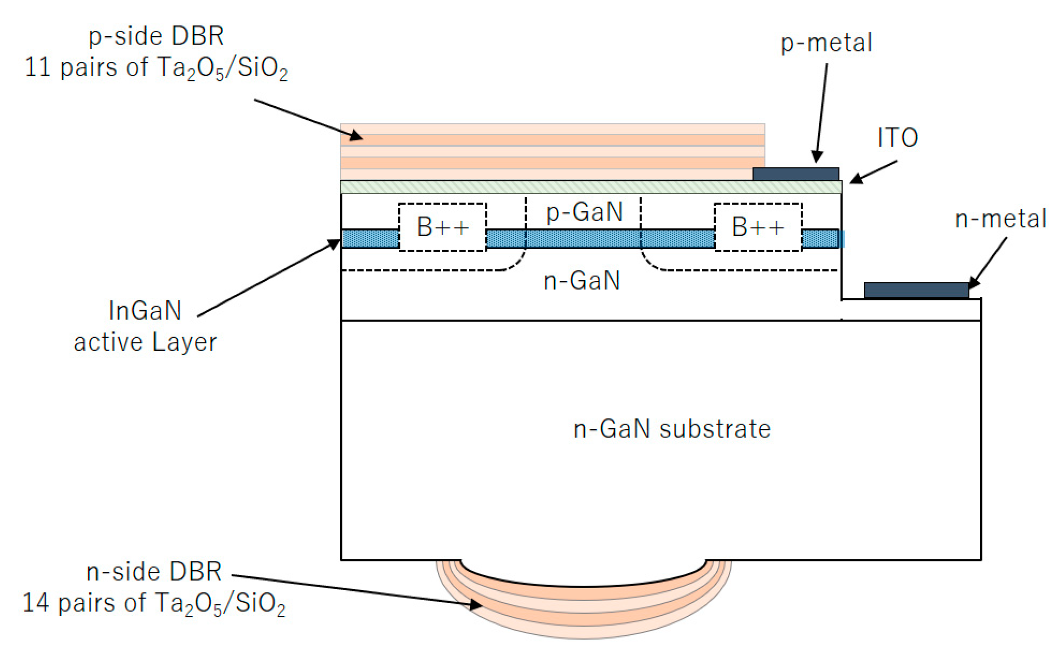
Figure 2 illustrates the device introduced in the present section. This unit was fabricated by first forming DBR islands consisting of 14.5 SiN/SiO2 bilayers on an n-GaN substrate, after which n-type GaN seed crystals were grown in the window regions between the DBR islands (where the GaN substrate was exposed) using MOCVD. As the MOCVD process progressed, these seeds grew in size, engulfing the DBR islands and finally forming planar surfaces above them. MOCVD was then used to grow four quantum wells a p-GaN layer and a contact layer, to a total thickness of approximately 100 nm. A 30-nm-thick indium tin oxide (ITO) layer and a p-side DBR with 11.5 Ta2O5/SiO2 bilayers were subsequently deposited on the contact layer and a Ti/Pt/Au n-electrode was overlaid on the bottom of the substrate. A circular current injection region with a diameter of 8 μm was electrically confined by boron ion implantation [15], where implanted boron (>1E19 cm−3) nullify electrical conductivity of GaN around the aperture. The cavity region was composed of the n-GaN layer grown over the DBR islands. The thickness of this n-GaN layer governed the cavity length of the device, which could be controlled to less than several microns by applying a predetermined growth rate.
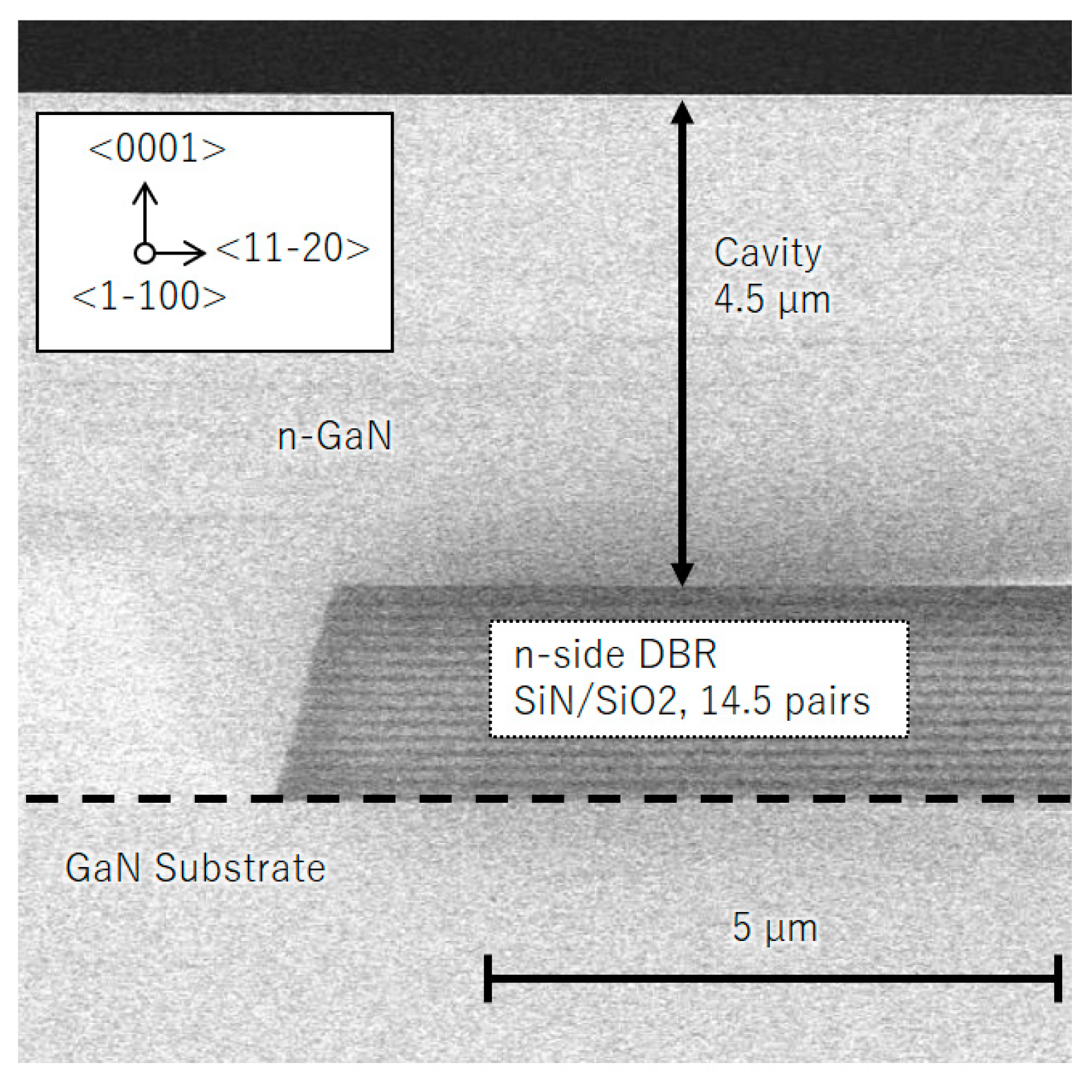
Figure 3 presents a cross-sectional SEM image of the ELO structure, in which an n-side DBR island was embedded inside an n-type GaN layer. This image demonstrates that the n-side DBR was completely embedded in the n-type GaN grown by the ELO technique. No cracks or voids are evident in or around the DBR and a planar surface that provides the basal plane for the p-side mirror is seen to have been formed above the n-side DBR. The distance from the surface of the epitaxial layer to the interface between the n-type GaN and n-side DBR was determined to be 4.5 μm, which corresponds to the cavity length for this device. The reflectance spectra generated from the top and bottom DBRs exhibited peak reflectance values of more than 99.9% and stopband widths of 80-97 nm. These widths are 4-5 times greater than those reported for nitride semiconductor DBRs.
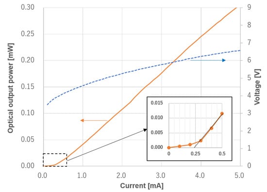
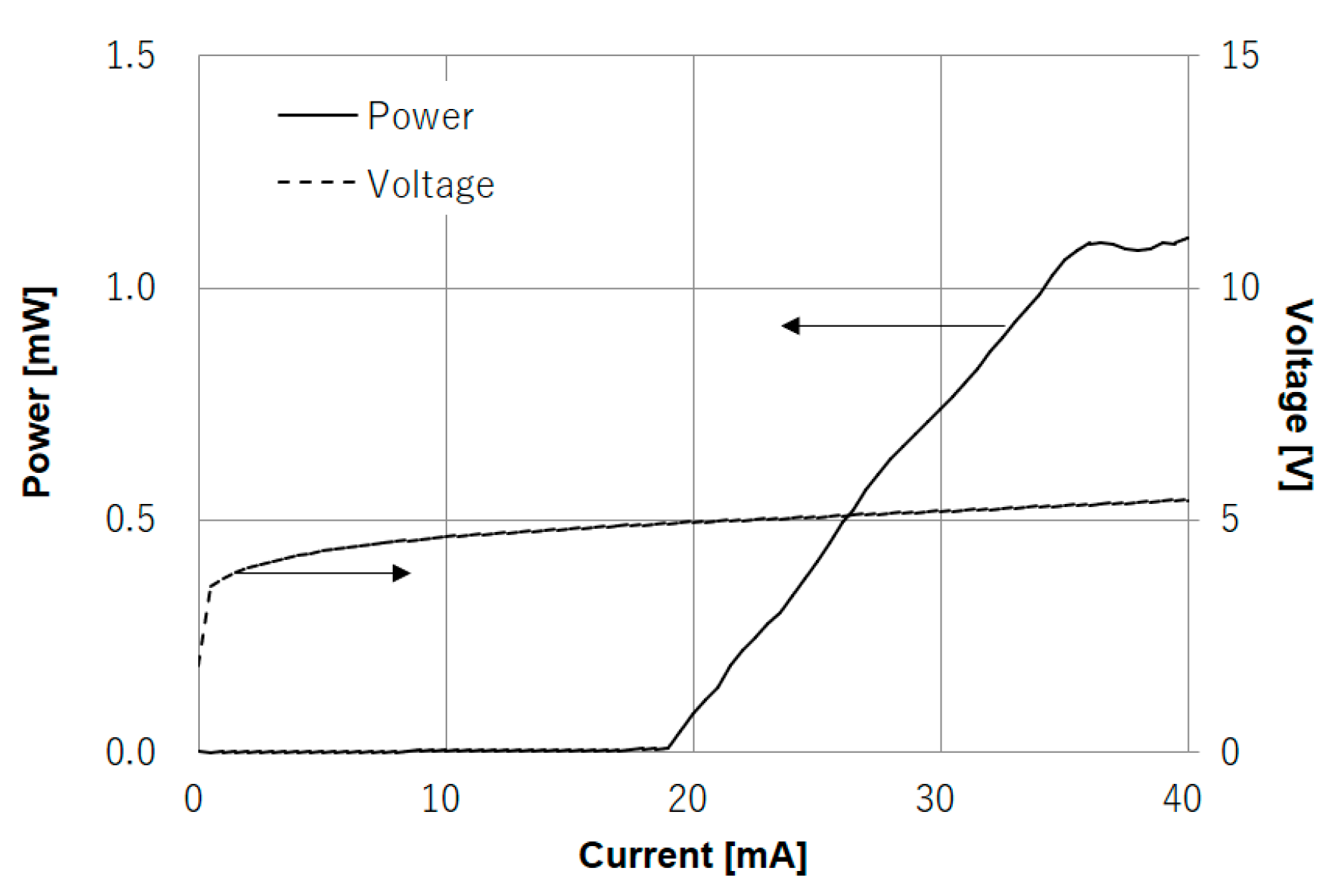
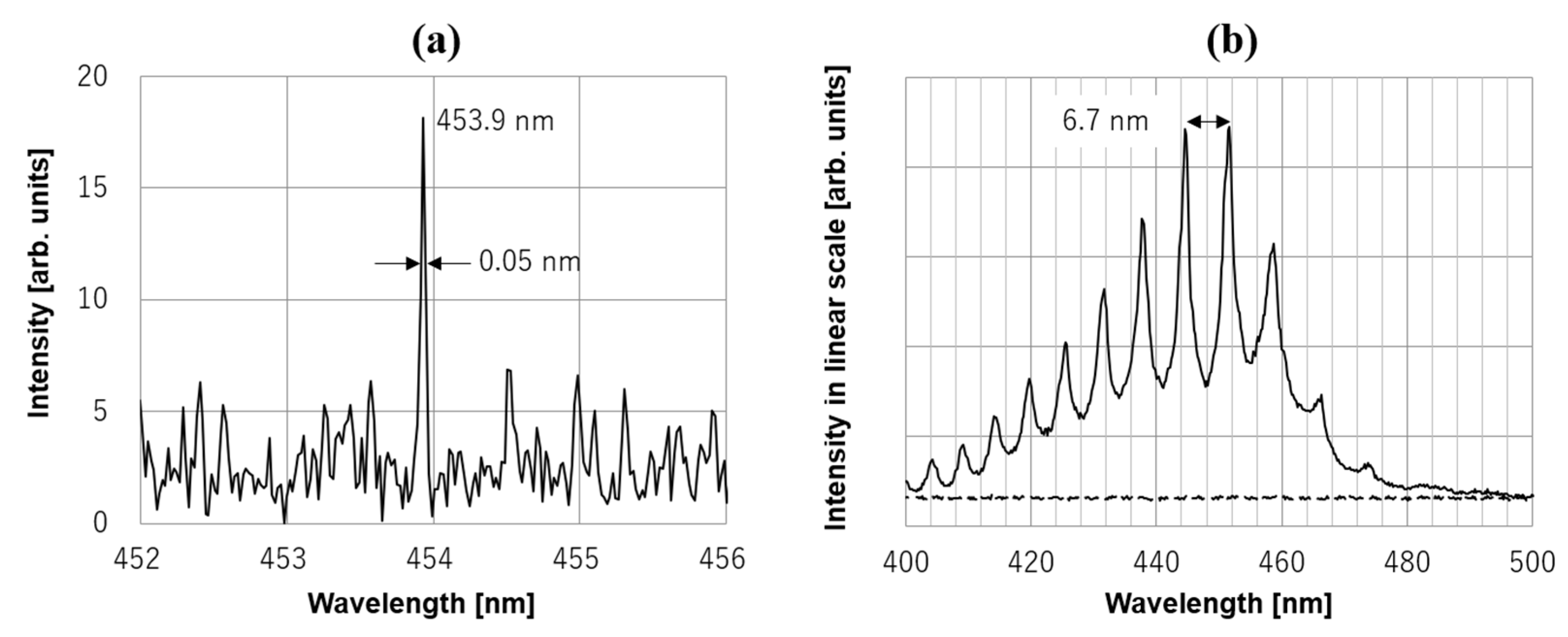
Figure 4 plots the current versus light output (I–L) and current versus voltage (I–V) curves for the device, for which the threshold current (Ith) and density (jth) were determined to be 18 mA and 35.8 kA cm−2, respectively. The maximum output power of this device was 1.1 mW. Figure 5 shows the spectra obtained below and above Ith and demonstrates a single longitudinal mode at a wavelength of 453.9 nm above Ith. The obvious threshold in the I–L curve and the fact that only a single longitudinal mode was observed above Ith demonstrate that lasing was achieved. The spacing of the longitudinal modes obtained below Ith was 6.7 nm (Figure 5), which is corresponding to cavity length of 4.5 µm by calculation for the following parameters: n = 2.45, λ = 450 nm, dn/dλ = −0.001. The obtained cavity length is consistent with the value measured by SEM (Figure 3).
As noted previously in this section, GaN-based nitrides have associated challenges in terms of obtaining DBRs having high reflectivity and a wide stopband and precise control of the fabrication process is required to obtain cavity lengths shorter than 10 μm. The VCSELs introduced in the present section met all these criteria. The DBRs at both ends of the cavity were made of dielectric materials that exhibit high reflectance over a wide spectral band width. It is preferable to determine the cavity length using the precise epitaxial growth afforded by MOCVD rather than to employ a more delicate process such as polishing, which was used in previous studies [8,9,10,11,12,13]. Figure 5a shows that the cavity length of 4.5 μm gives a diffraction loss per round trip of much less than 1% at a variety of aperture sizes. The ELO process that is primarily responsible for the formation of the cavity can be implemented uniformly over a large area of the wafer. Thus, this process enables the fabrication of multiple devices on a single wafer, which makes it very suitable for mass production.
6. All-dielectric-DBR GaN-based VCSELs Using an Atomically Smooth Monolithic Curved Mirror
As discussed in Section 4, one approach to overcoming potential problems associated with all-dielectric DBR VCSELs is to introduce lateral optical confinement, which allows the use of relatively long cavities (greater than 10 μm) with no diffraction loss. There have been a few studies on this topic regarding GaN-VCSELs. Hashemi et al. simulated the effect of lateral optical confinement by step-like lateral structures on the internal losses of GaN-VCSELs [27]. In addition, Hayashi et al. experimentally demonstrated one of those structures and found that the multi-lateral-mode of the device provided evidence for lateral optical guiding [21]. Kuramoto et al. reported improved slope efficiency in the case of a device incorporating a mesa structure [22], which confirmed the effect of lateral optical confinement of the cavity.
However, those step-like lateral structures also induced scattering losses. For this reason, the authors of the present review proposed a GaN-VCSEL having a cavity with a graded lateral structure instead of a mesa structure. Resonators cladded with curved and plane mirrors are known to form stable cavities without diffraction and scattering losses, in association with the generation of a beam waist on the plane mirror [28]. Thus, the introduction of curved mirrors on one side of the VCSEL may allow for longer cavities that would help to relax the strict processing requirements during polishing that have prevented GaN-VCSELs from being mass produced. The first experimental result based on this concept was reported following work with GaN-VCSELs by Park et al. [29], who investigated the optical pumping of devices having 50-μm-long cavities with plane and curved end mirrors. InGaN quantum wells were grown epitaxially on the (0001) plane of a sapphire template (t = 50 μm) to fabricate these devices and a monolithic curved mirror was generated on the (000-1) plane of the template using ball-up resin patterns as sacrificial masks during the reactive ion etching of the sapphire. However, this study only demonstrated laser operation in conjunction with optical pumping.
The author’s group investigated lasing as a result of current injection into VCSELs with a similar structure, in which InGaN wells were grown epitaxially on (0001) GaN substrates and a curved mirror was fabricated on (000-1) GaN rather than on sapphire substrates (see Figure 6) [16]. These devices were fabricated by growing three InGaN/GaN MQWs via MOCVD, a p-GaN layer doped with Mg (approximately 1 × 1019 cm−3) and a contact layer doped with Mg (approximately 1 × 1020 cm−3), to a total thickness of 105 nm, on a (0001) GaN substrate. A 20-nm-thick ITO layer and a p-side DBR with 11.5 Ta2O5/SiO2 bilayers were deposited on the contact layer. A hole was etched next to the aperture, reaching the n-GaN layer and two Ti/Pt/Au electrodes were deposited so that they made contact with the ITO layer and the exposed n-GaN, respectively, to form a current path. A circular current injection region was electrically confined by boron implantation, leaving a current aperture with a diameter of 3 μm that was in contact with the ITO and one Ti/Pt/Au electrode to form an emitter. The remaining processing steps during fabrication of the curved mirror were similar to those used in Parks’ research. That is, ball-up resin patterns were employed as sacrificial masks during reactive ion etching of the GaN substrate.
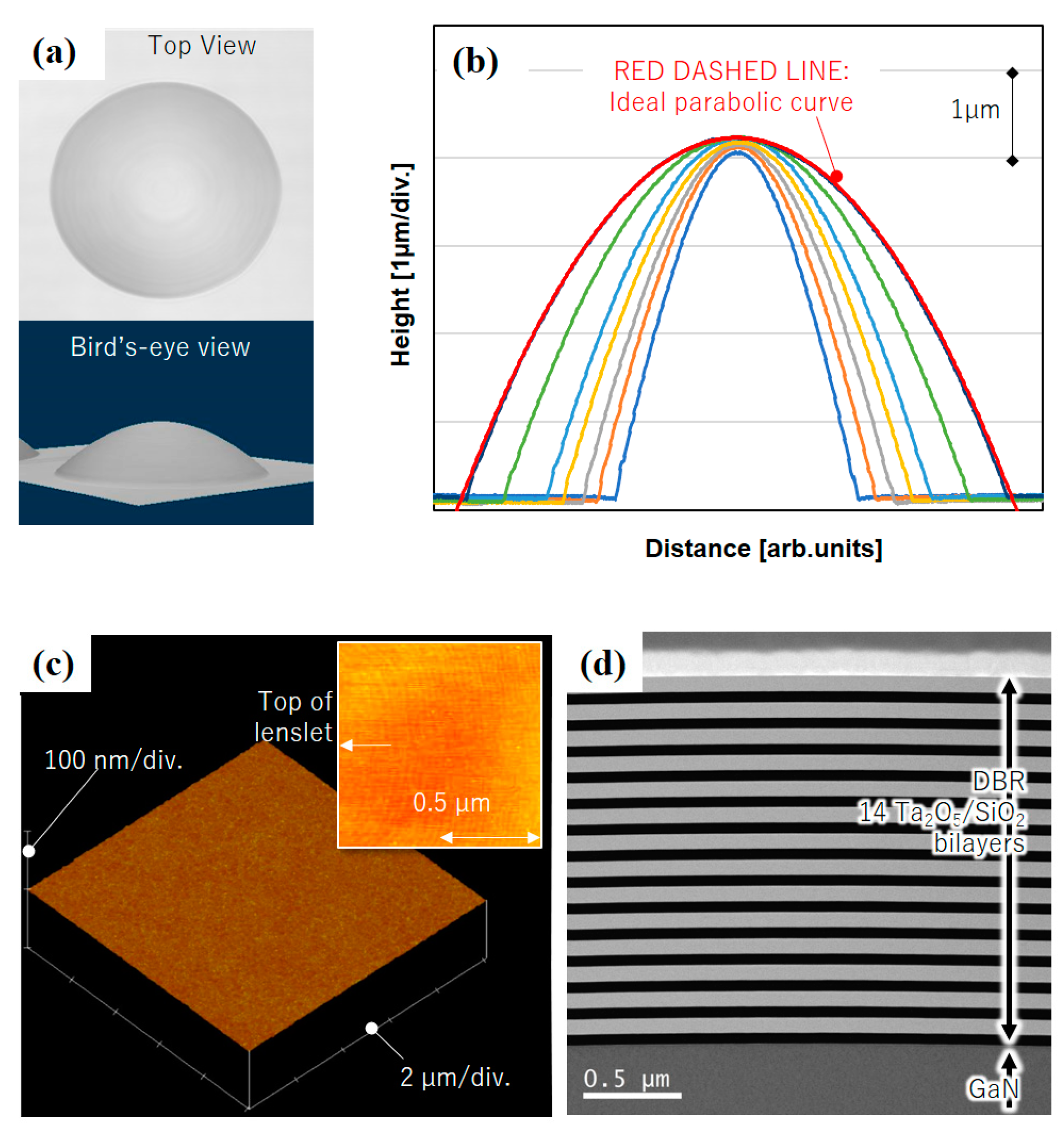
Figure 7a,b show laser confocal microscopy images of a lenslet fabricated on the (000-1) plane of a GaN substrate fabricated through these procedures. The top and bird’s-eye views in Figure 7a both demonstrate the smooth droplet shape that was formed. In the cross-sectional analysis (Figure 7b), an ideal parabolic curve has been overlaid on the experimentally determined cross-sections. An atomic force microscopy (AFM) image of the top of the lenslet is shown in Figure 7c. The root mean square roughness of this surface was determined to be 0.2 nm, which is comparable to the value reported for a plane mirror that allowed lasing from a GaN-VCSEL in a prior study [30]. This image also clearly shows atomic steps at the top of the lenslet (inset to Figure 7c), indicating the minimal roughness of this surface. Figure 7d presents a transmission electron microscopy (TEM) image of the cross-section of the curved mirror in this device. Each DBR layer is seen to bend smoothly across the top of the lenslet formed on the GaN, forming a perfect curved mirror.
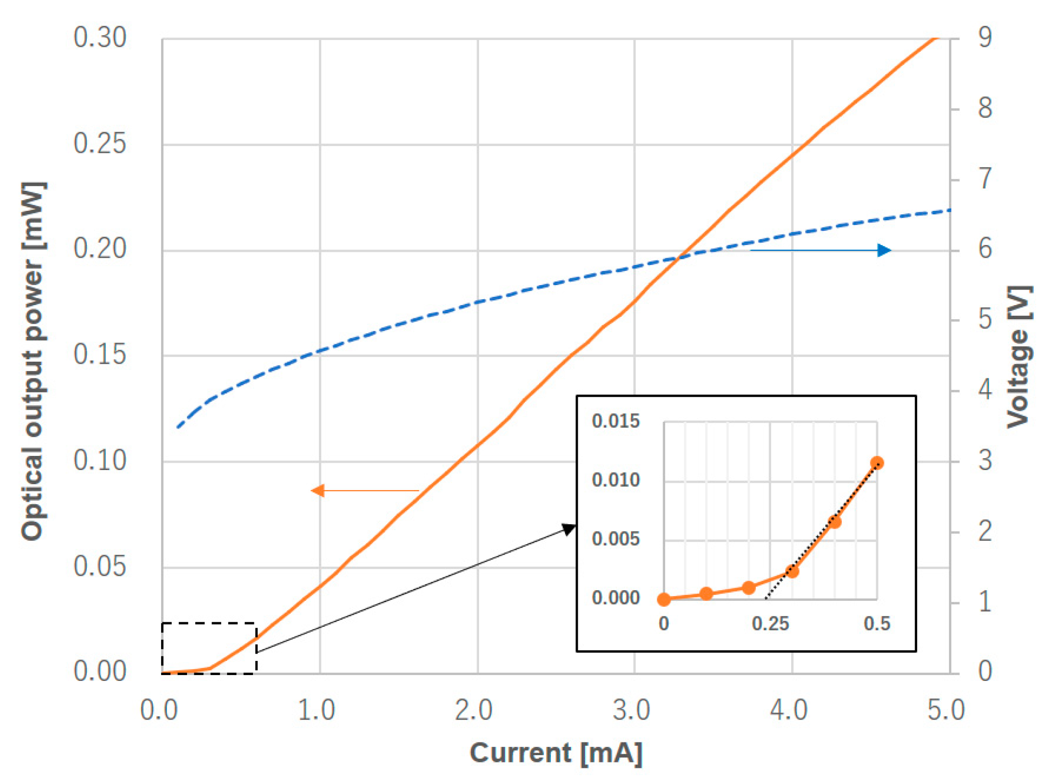
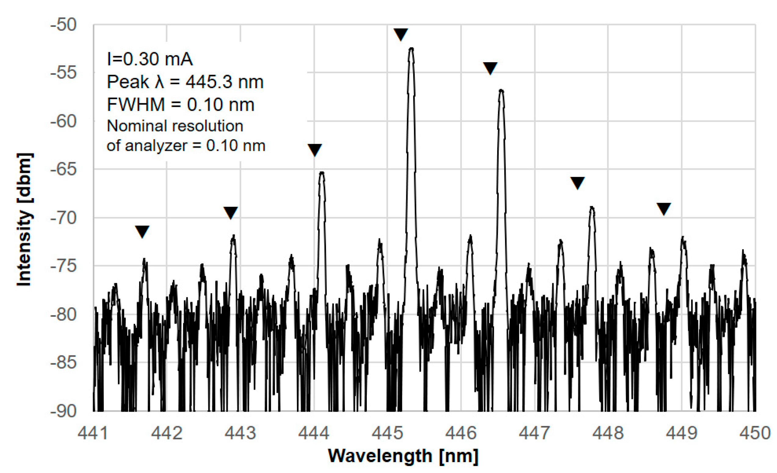
Figure 8 shows the current-voltage (I-V) and current-optical output (I-L) curves for the GaN-VCSEL device. The I-L curve exhibits a clear threshold at an injected current of 0.25 mA (Jth = 3.5 kA/cm2 for a current aperture diameter of 3 µm) during CW injection. Figure 9 provides the emission spectrum for the device above the threshold current, which exhibits a dominant peak at a wavelength of 445.3 nm. The width of this spectrum is equivalent to the resolution limit of the analyzer (0.1 nm). The emission spectrum contains multiple peaks and the primary peaks are spaced at intervals of 1.27 nm, as indicated by the filled triangles. This interval corresponds to the mode spacing calculated for a cavity length of 27 µm when using n = 2.45, λ = 445.3 nm and dn/dλ = −0.001 [16]. This result demonstrates that the lasing occurred with multi-longitudinal modes. The dimensional parameters for this device were determined to be L = 27 µm using scanning electron microscopy (data not shown) and R = 29.1 µm using confocal laser microscopy. According to classic Gaussian optics theory [16], this cavity had an associated resonant mode with a beam waist (4σ) of 1.3 µm on the planar mirror. This value is smaller than the current injection diameter of 3 µm.
The research described above confirmed the appearance of a near field image and the beam waist matched the theoretically predicted shape, demonstrating that the resonant mode was confined in the lateral direction, as predicted by Gaussian optics. Because a small aperture of 1 to 2 µm in conjunction with a cavity longer than 20 µm should result in a large diffraction loss (up to approximately 100%) per round trip (see Figure 2a), the previously discussed small threshold current strongly suggests the occurrence of lateral optical confinement in this type of GaN-based VCSEL.
7. Conclusions
This review described a variety of possible GaN-based VCSEL structures. The initial section concentrated on early prototypes, of which there were two main types: hybrid-DBR and all-dielectric-DBR. Although both types exhibit lasing during CW operation in conjunction with current injection, there are challenges associated with mass production. Specifically, it is difficult to control the thicknesses of each nitride semiconductor layer in the DBRs in hybrid-DBR types and the size of the cavity itself in all-dielectric-DBR devices. The latter part of this document reviewed two types of novel all-dielectric GaN-based VCSELs having different structures. One such device incorporates dielectric DBRs at either end of the cavity, with one side of each DBR embedded in n-type GaN grown using ELO. The other type incorporates a curved mirror fabricated on (000-1) GaN. These designs are intended to eliminate the requirement for strict control of the cavity length and to address the absence of lateral optical confinement, both of which have prevented the practical use of all-dielectric GaN-based VCSELs.
As discussed throughout this paper, a variety of structures have been reported for GaN-based VCSELs during the research history spanning approximately 10 years. As a result of this short period of time, as of 2018, hybrid-DBR GaN-based VCSELs have been developed that exhibit wall plug efficiencies close to 10%, while all-dielectric-DBR devices have shown threshold currents much lower than 1 mA. The authors believe that additional research activity will improve the performance of GaN-based VCSELs and allow their practical use in the near future.
Author Contributions
T.H. has written the manuscript following advices given by N.F. and H.N.
Funding
This research received no external funding.
Acknowledgments
The authors are grateful to the following colleagues who have worked on the development of GaN-based VCSELs at the Sony Corporation: Izumi, Murayama, Mitomo, Satou, Fujii, Watanabe, Jyoukawa, Ito, Kobayashi, Ohara, Kawanishi, Koda, Narui and Yanashima. The authors thank Takeuchi, for his helpful advice during the writing of this paper and Fujioka, for providing the opportunity to produce this review.
Conflicts of Interest
The contents of this paper are based on the authors’ knowledge acquired though research activity as employees of the Sony Corporation.
References
- Akasaki, I.; Amano, H. Breakthroughs in Improving Crystal Quality of GaN and Invention of the p–n Junction Blue-Light-Emitting Diode. J. Appl. Phys. 2006, 45, 12. [Google Scholar] [CrossRef]
- Nakamura, S.; Senoh, M.; Nagahama, S.; Iwasa, N.; Yamada, T.; Matsushita, T.; Sugimoto, Y.; Kiyoku, H. Room-temperature continuous-wave operation of InGaN multi-quantum-well structure laser diodes. Appl. Phys. Lett. 1996, 69, 4056. [Google Scholar] [CrossRef]
- Takeuchi, T.; Kamiyama, S.; Iwaya, M.; Akasaki, I. GaN-based vertical-cavity surface-emitting lasers with AlInN/GaN distributed Bragg reflectors. Rep. Prog. Phys. 2019, 82, 1. [Google Scholar] [CrossRef] [PubMed]
- Lu, T.C.; Kao, C.C.; Kuo, H.C.; Huang, G.S.; Wang, S.C. CW lasing of current injection blue GaN-based vertical cavity surface emitting laser. Appl. Phys. Lett. 2008, 92, 141102. [Google Scholar] [CrossRef]
- Lu, T.C.; Chen, S.W.; Wu, T.T.; Tu, P.M.; Chen, C.K.; Chen, C.H.; Li, Z.Y.; Kuo, H.C.; Wang, S.C. Continuous wave operation of current injected GaN vertical cavity surface emitting lasers at room temperature. Appl. Phys. Lett. 2010, 97, 071114. [Google Scholar] [CrossRef]
- Carlin, J.F.; Dorsaz, J.; Feltin, E.; Butte, R.; Grandjean, N.; Ilegems, M. Crack-free fully epitaxial nitride microcavity using highly reflective AlInNGaN Bragg mirrors. Appl. Phys. Lett. 2005, 86, 031107. [Google Scholar] [CrossRef]
- Kozuka, Y.; Ikeyama, K.; Yasuda, T.; Takeuchi, T.; Kamiyama, S.; Iwaya, M.; Akasaki, I. Growths of AlInN Single Layers and Distributed Bragg Reflectors for VCSELs. MRS Proc. 2015, 1736. [Google Scholar] [CrossRef]
- Higuchi, Y.; Omae, K.; Matsumura, H.; Mukai, T. Room-Temperature CW Lasing of a GaN-Based Vertical-Cavity Surface-Emitting Laser by Current Injection. Appl. Phys. Express 2008, 1, 121102. [Google Scholar] [CrossRef]
- Omae, K.; Higuchi, Y.; Nakagawa, K.; Matsumura, H.; Mukai, T. Improvement in Lasing Characteristics of GaN-based Vertical-Cavity Surface-Emitting Lasers Fabricated Using a GaN Substrate Kunimichi. Appl. Phys. Express 2009, 2, 052101. [Google Scholar] [CrossRef]
- Kasahara, D.; Morita, D.; Kosugi, T.; Nakagawa, K.; Kawamata, J.; Higuchi, Y.; Matsumura, H.; Mukai, T. Demonstration of Blue and Green GaN-Based Vertical-Cavity Surface-Emitting Lasers by Current Injection at Room Temperature. Appl. Phys. Express 2011, 4, 072103. [Google Scholar] [CrossRef]
- Kasahara, D.; Marui, H.; Kawamata, J.; Kosugi, T.; Higuchi, Y.; Nagahama, S. Pure green 529 nm room-temperature lasing of GaN-based vertical-cavity surface-emitting Laser by current injection. In Proceedings of the 1st Laser Display Conference, Yokohama, Japan, 26–27 April 2012. [Google Scholar]
- Liu, W.J.; Hu, X.L.; Ying, L.Y.; Zhang, J.Y.; Zhang, B.P. Room temperature continuous wave lasing of electrically injected GaN-based vertical cavity surface emitting lasers. Appl. Phys. Lett. 2014, 104, 251116. [Google Scholar] [CrossRef]
- Onishi, T.; Imafuji, O.; Nagamatsu, K.; Kawaguchi, M.; Yamanaka, K.; Takigawa, S. Continuous Wave Operation of GaN Vertical Cavity Surface Emitting Lasers at Room Temperature. IEEE J. Quant. Electron. 2012, 48, 1107. [Google Scholar] [CrossRef]
- Hamaguchi, T.; Fuutagawa, N.; Izumi, S.; Narui, H. Milliwatt-class GaN-based blue vertical-cavity surface-emitting lasers fabricated by epitaxial lateral overgrowth. Phys. Status Solidi 2016, 213, 1170. [Google Scholar] [CrossRef]
- Hamaguchi, T.; Nakajima, H.; Ito, M.; Mitomo, J.; Satou, S.; Fuutagawa, N.; Narui, H. Lateral carrier confinement of GaN-based vertical-cavity surface-emitting diodes using boron ion implantation. Jpn. J. Appl. Phys. 2016, 55, 12. [Google Scholar] [CrossRef]
- Hamaguchi, T.; Tanaka, M.; Mitomo, J.; Nakajima, H.; Ito, M.; Ohara, M.; Kobayashi, N.; Fujii, K.; Watanabe, H.; Satou, S.; et al. Lateral optical confinement of GaN- based VCSEL using an atomically smooth monolithic curved mirror. Sci. Rep. 2018, 8, 10350. [Google Scholar] [CrossRef] [PubMed]
- Hamaguchi, T.; Nakajima, H.; Tanaka, M.; Ito, M.; Ohara, M.; Jyoukawa, T.; Kobayashi, N.; Matou, T.; Hayashi, K.; Watanabe, H.; et al. Sub-milliampere-threshold continuous wave operation of GaN-based vertical-cavity surface-emitting laser with lateral optical confinement by curved mirror. Appl. Phys. Express 2019. [Google Scholar] [CrossRef]
- Koyama, F.; Kinoshita, S.; Iga, K. Room temperature CW operation of GaAs vertical cavity surface emitting laser. IEICE Trans. 1988, 71, 1089–1090. [Google Scholar]
- Coldren, L.A. Vertical-Cavity Surface-Emitting Lasers; Cambridge University Press: Cambridge, UK, 1999. [Google Scholar]
- Choquette, K.D.; Schneider, R.P.; Lear, K.L.; Geib, K.M. Low threshold voltage vertical-cavity lasers fabricated by selective oxidation. Electron. Lett. 1994, 30, 2043. [Google Scholar] [CrossRef]
- Hayashi, N.; Ogimoto, J.; Matsui, K.; Furuta, T.; Akagi, T.; Iwayama, S.; Takeuchi, T.; Kamiyama, S.; Iwaya, M.; Akasaki, I. A GaN-Based VCSEL with a Convex Structure for Optical Guiding. Phys. Status Solidi 2018, 215, 1700648. [Google Scholar] [CrossRef]
- Kuramoto, M.; Kobayashi, S.; Akagi, T.; Tazawa, K.; Tanaka, K.; Saito, T.; Takeuchi, T. Enhancement of slope efficiency and output power in GaN-based vertical-cavity surface-emitting lasers with a SiO2-buried lateral index guide Masaru. Appl. Phys. Lett. 2018, 112, 111104. [Google Scholar] [CrossRef]
- Witzigmann, B.; Laino, V.; Luisier, M.; Schwarz, U.T.; Feicht, G.; Wegscheider, W.; Engl, K.; Furitsch, M.; Leber, A.; Lell, A.; et al. Microscopic analysis of optical gain in InGaN∕GaN quantum wells. Appl. Phys. Lett. 2006, 88, 021104. [Google Scholar] [CrossRef]
- Leonard, J.T.; Cohen, D.A.; Yonkee, B.P.; Farrell, R.M.; Margalith, T.; Lee, S.; DenBaars, S.P.; Speck, J.S.; Nakamura, S. Nonpolar III-nitride vertical-cavity surface-emitting lasers incorporating an ion implanted aperture. Appl. Phys. Lett. 2015, 107, 011102. [Google Scholar] [CrossRef]
- Izumi, S.; Fuutagawa, N.; Hamaguchi, T.; Murayama, M.; Kuramoto, M.; Narui, H. Room-temperature continuous-wave operation of GaN-based vertical-cavity surface-emitting lasers fabricated using epitaxial lateral overgrowth. Appl. Phys. Express 2015, 8, 062702. [Google Scholar] [CrossRef]
- Okur, S.; Shimada, R.; Zhang, F.; Hafiz, S.D.A.; Lee, J.; Avrutin, V.; Morkoç, H.; Franke, A.; Bertram, F.; Christen, J.; Özgür, Ü. GaN-Based Vertical Cavities with All Dielectric Reflectors by Epitaxial Lateral Overgrowth. Jpn. J. Appl. Phys. 2013, 52, 08JH03. [Google Scholar] [CrossRef]
- Hashemi, E.; Gustavsson, J.; Bengtsson, J.; Stattin, M.; Cosendey, G.; Grandjean, N.; Haglund, Å. Engineering the Lateral Optical Guiding in Gallium Nitride-Based Vertical-Cavity Surface-Emitting Laser Cavities to Reach the Lowest Threshold Gain. Jpn. J. Appl. Phys. 2013, 52, 08JG04. [Google Scholar] [CrossRef]
- Kogelnik, H.; Li, T. Laser Beams and Resonators. Appl. Opt. 1966, 10, 1550. [Google Scholar] [CrossRef] [PubMed]
- Park, S.; Kim, J.; Sakong, H.J.; Lee, S.N.; Chae, S.; Jeong, Y.P.; Cho, G.Y. Room-temperature GaN vertical-cavity surface-emitting laser operation in an extended cavity scheme. Appl. Phys. Lett. 2003, 83, 15. [Google Scholar] [CrossRef]
- Liu, W.; Chen, S.; Hu, X.; Liu, Z.; Zhang, J.; Ying, L.; Lv, X.; Akiyama, H.; Cai, Z.; Zhang, B. Low Threshold Lasing of GaN-Based VCSELs With Sub-Nanometer Roughness Polishing. IEEE Photon. Technol. Lett. 2013, 25, 20. [Google Scholar] [CrossRef]
Figure 1.
(a) Calculated coupling (diffraction) losses per round trip for beams having Gaussian lateral profiles with a beam waist from 1 to 10 μm. (b) Longitudinal mode spacing calculated for the parameters n = 2.45, λ = 450 nm and dn/dλ = −0.001 [16].
Figure 1.
(a) Calculated coupling (diffraction) losses per round trip for beams having Gaussian lateral profiles with a beam waist from 1 to 10 μm. (b) Longitudinal mode spacing calculated for the parameters n = 2.45, λ = 450 nm and dn/dλ = −0.001 [16].

Figure 2.
Schematic of an all-dielectric-distributed Bragg reflectors (DBR) gallium nitride based (GaN)-based VCSEL in which the bottom side DBR is encased in n-GaN generated using an epitaxial lateral overgrowth technique.
Figure 2.
Schematic of an all-dielectric-distributed Bragg reflectors (DBR) gallium nitride based (GaN)-based VCSEL in which the bottom side DBR is encased in n-GaN generated using an epitaxial lateral overgrowth technique.

Figure 3.
Cross-sectional scanning electron microscopy (SEM) image of the epitaxial lateral overgrowth (ELO) structure, in which the n-side DBR is engulfed in n-GaN grown using the ELO process. The flat surface of the epitaxial layer forms a 4.5-mm-long cavity.
Figure 3.
Cross-sectional scanning electron microscopy (SEM) image of the epitaxial lateral overgrowth (ELO) structure, in which the n-side DBR is engulfed in n-GaN grown using the ELO process. The flat surface of the epitaxial layer forms a 4.5-mm-long cavity.

Figure 4.
I–V and I–L curves generated by an all-dielectric-DBR GaN-based vertical-cavity surface-emitting laser (VCSEL). Here, Ith was 18 mA and the maximum output power was 1.1 mW, the highest value reported to date for this type of device. The kinks in the I–L curve suggest multimodal operation for the lateral mode, presumably due to the absence of lateral optical confinement.

Figure 5.
Spectra obtained from the all-dielectric-DBR GaN-based VCSEL above and below the threshold current (18 mA). Spectrum (a) was obtained at 20 mA and shows a single longitudinal mode at 453.9 nm and a half width at maximum of 0.05 nm. The latter value is equivalent to the resolution limit of the apparatus used to acquire the data (ADCMT8341). Spectrum (b) was acquired at 10 mA using a different spectrum analyzer (Ocean Optics USB4000) and shows a mode spacing of 6.7 nm.

Figure 6.
Schematic of a GaN-VCSEL having a curved mirror [16].
Figure 6.
Schematic of a GaN-VCSEL having a curved mirror [16].

Figure 7.
(a) Laser scanning confocal microscope images and (b) cross-sectional profiles of lenslets fabricated on the (000-1) plane of GaN wafers. In (b), multiple profiles acquired from specimens having different diameters are overlaid, while the red dashed line is an ideal parabolic curve fitted to one of the plots. (c) AFM image of the top of a lenslet fabricated on the (000-1) plane of a GaN substrate. The inset is a high-resolution image of a 1 μm × 1 um area that shows atomic steps on the surface. (d) Cross-sectional TEM image of the curved mirror of the device used for an optical pumping test.

Figure 8.
I-V and I-L curves obtained from a GaN-VCSEL with a 3 µm aperture at room temperature in response to continuous current injection. The inset shows an enlarged view of the data around the threshold current.
Figure 8.
I-V and I-L curves obtained from a GaN-VCSEL with a 3 µm aperture at room temperature in response to continuous current injection. The inset shows an enlarged view of the data around the threshold current.

Figure 9.
Emission spectrum generated by a GaN-VCSEL with a threshold current of 0.25 mA in response to a current injection of 0.30 mA.
Figure 9.
Emission spectrum generated by a GaN-VCSEL with a threshold current of 0.25 mA in response to a current injection of 0.30 mA.

© 2019 by the authors. Licensee MDPI, Basel, Switzerland. This article is an open access article distributed under the terms and conditions of the Creative Commons Attribution (CC BY) license (http://creativecommons.org/licenses/by/4.0/).
Share and Cite
MDPI and ACS Style
Hamaguchi, T.; Nakajima, H.; Fuutagawa, N. GaN-based Vertical-Cavity Surface-Emitting Lasers Incorporating Dielectric Distributed Bragg Reflectors. Appl. Sci. 2019, 9, 733. https://0-doi-org.brum.beds.ac.uk/10.3390/app9040733
AMA Style
Hamaguchi T, Nakajima H, Fuutagawa N. GaN-based Vertical-Cavity Surface-Emitting Lasers Incorporating Dielectric Distributed Bragg Reflectors. Applied Sciences. 2019; 9(4):733. https://0-doi-org.brum.beds.ac.uk/10.3390/app9040733
Chicago/Turabian StyleHamaguchi, Tatsushi, Hiroshi Nakajima, and Noriyuki Fuutagawa. 2019. "GaN-based Vertical-Cavity Surface-Emitting Lasers Incorporating Dielectric Distributed Bragg Reflectors" Applied Sciences 9, no. 4: 733. https://0-doi-org.brum.beds.ac.uk/10.3390/app9040733
Note that from the first issue of 2016, this journal uses article numbers instead of page numbers. See further details here.