Micro-LEDs, a Manufacturability Perspective


Department of Electrical and Computer Engineering, Virginia Commonwealth University, 601 West Main Street, Richmond, VA 23284, USA
*
Author to whom correspondence should be addressed.
Appl. Sci. 2019, 9(6), 1206; https://0-doi-org.brum.beds.ac.uk/10.3390/app9061206
Submission received: 26 February 2019
/
Revised: 18 March 2019
/
Accepted: 20 March 2019
/
Published: 22 March 2019
(This article belongs to the Special Issue Group III-V Nitride Semiconductor Microcavities and Microemitters)
Abstract
:Compared with conventional display technologies, liquid crystal display (LCD), and organic light emitting diode (OLED), micro-LED displays possess potential advantages such as high contrast, fast response, and relatively wide color gamut, low power consumption, and long lifetime. Therefore, micro-LED displays are deemed as a promising technology that could replace LCD and OLED at least in some applications. While the prospects are bright, there are still some technological challenges that have not yet been fully resolved in order to realize the high volume commercialization, which include efficient and reliable assembly of individual LED dies into addressable arrays, full-color schemes, defect and yield management, repair technology and cost control. In this article, we review the recent technological developments of micro-LEDs from various aspects.
1. Introduction
Owing to the fact that III-nitride-based light-emitting diodes (LEDs) are more efficient, reliable, and have longer life span in comparison to traditional lighting sources, such as incandescent and fluorescent bulbs, they are increasingly being employed as an energy-saving solution for various applications, among which are general lighting, automobile, signal, and backlighting in displays. Conventionally, to provide sufficient light power for general lighting, lateral dimensions of LED chips are designed to be larger than 200 μm × 200 μm. However, various emerging display applications, including wearable devices, head-mounted, and large-area displays require miniaturized chips composed of arrays of micro-scale LED elements (micro-LED) with high density with the lateral dimension down to less than 100 μm × 100 μm [1,2,3,4,5]. Due to the benefits provided by miniaturization, micro-LEDs are considered to possess great potential in multi-site neuron stimulation [6,7], miniaturized optoelectronic tweezers [8], optical cochlear implants [9], and mask-free lithography [10]. Additionally, a short differential carrier lifetime resulting from reduced capacitance and increased current density in micro-LEDs makes it also an appealing candidate for high-speed visible light communications (VLC) [11,12,13,14].
Today, the mainstream flat panel displays (FPDs) are dominated by liquid crystal display (LCDs) and organic light emitting diodes (OLEDs). Traditional LCD display requires LED backlight to emit light through a matrix of liquid crystal to generate images, and it suffers from the issues of high power consumption, slow response time, low viewing angle, and low uniformity. Unlike LCDs, OLED displays are self-emissive, and each pixel can be switched on and off individually. However, due to its inorganic nature, it has limitations in brightness and stability. Compared with them, micro-LED displays possess potential advantages such as high contrast, fast response, and relatively wide color gamut, low power consumption, and long lifetime. The prospects of a wide range of applications of micro-LEDs have attracted a large number of manufactures, startups, and academic researchers to establish programs in the field. Setting the display applications aside, since the early 2000s, micro-LEDs have been investigated to improve the luminescence efficiency for high-intensity lighting motivated by their relatively high light extraction efficiency, better current spreading, and lower self-heating effect [15,16,17,18]. In recent years, tens of companies around the world have been involved in the micro-LED technology. For instance, Sony demonstrated its first 55" full-HD micro-LED TV panel in 2012, which featured six million micro-LEDs. Compared with the existing Sony LCD and plasma displays, the micro-LED prototype features 3.5 times higher contrast ratio, 1.4 times wider color gamut, and 10 times faster response time. In 2018, Sony released its micro-LED crystal-LED “CLEDIS” integrated display with micro-LED chip size of 0.003 mm2, which has a contrast ratio of over 1,000,000:1 and a black surface area of over 99%. CEA-Leti, a technology research institute in France, demonstrated its prototype wide video graphic array (WVGA) micro-display with 10 μm pixel pitch in 2017, which is based on the patterning of monochrome (blue or green) GaN micro-LED arrays and hybridizing with complementary metal-oxide-semiconductor (CMOS) circuit. In 2018, PlayNitride demonstrated two full-color micro-LED prototypes, one is a 0.89 inch 64 × 64 panel with 105 pixel per inch (PPI) resolution, and another is a 3.12 inch 256 × 256 panel with 116 PPI resolution. AU Optronics Corp. has demonstrated 12.1 inch full-color micro-LED display with a 169 PPI and 1920 × 720 resolution achieved by micro-LEDs with pixel size less than 30 microns. X-Celeprint has demonstrated both passive and active matrix full-color micro-LED displays. In 2018, a 5.1 inch full-color micro LED display with active-matrix switching, which was made of 8 × 15 micron red, green, and blue LEDs with a 70 PPI was presented. However, high volume commercialization of micro-LED displays has not yet been reported.
While the science is clear, new technical challenges arise when the chip size shrinks and chip density expands. To conquer the related challenges, new techniques have been developing from the ongoing investigations. There are a few recent review papers that have addressed the status of micro-LED landscape, but have not sufficiently addressed the technological developments [1,19]. In this article, we overview the techniques in the key areas including mass transfer, monolithic fabrication, and full-color realization. Current bottlenecks and likelihood of overcoming them are also discussed.
2. Epitaxy and Chip Processing
The main requirements on the epitaxial growth aspects of GaN-based micro-LEDs are the wavelength and drive current homogeneity across the wafer and low defect density. Both Aixtron and Veeco, two major manufacturers of deposition systems, have articulated their approaches to address the particular needs for epitaxy of micro-LEDs [20,21]. Aixtron’s Planetary Reactor® technology uses Gas Foil Rotation® for each wafer disks to enable uniform growth across an individual wafer and a second rotation to improve wafer-to-wafer uniformity [20]. By incorporating a Cl2 in situ cleaning process between each run and cassette-to-cassette wafer automation, a density of defects (with a size larger than 1 μm) as low as ~0.1 defects/cm2 has been achieved. Veeco’s vertical-rotating disc TurboDisc™ technology provides high 14 × 6” capacity with low defectivity and high uniformity [21]. A defectivity yield (percentage of killer defect number ≤ 1 per Epi donor field) above 90% has been demonstrated for applications in smartphones and TVs, respectively.
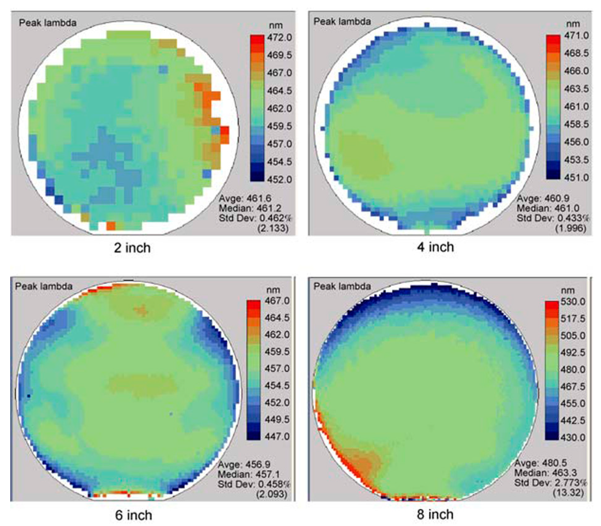
Desire for large diameter sapphire substrates to meet the needs of large-sized monolithic micro-displays brings about some difficulties due to increased bowing induced by the large thermal and lattice mismatches with the LED epilayer structure [22,23]. The primary problem associated with wafer bowing is non-uniformity of the wafer surface temperature resulting in the spatially non-uniform distribution of the indium molar fractions in the InGaN/GaN MQWs over the wafer. A temperature non-uniformity of 1 °C could induce a wavelength variation of 1.8 and 2.5 nm in blue and green LEDs, respectively [24]. Wafer bowing also causes issues during the device fabrication process, such as wafer cracking and degradation of device homogeneity in dry etching and other like processes. To deal with these challenges, thicker substrates, optimized wafer holder designs, control of the coalescence stage, insertion of strain-compensation layers, and internally focused laser treatment, have been employed and or investigated [23,24,25,26,27]. For example, Lu et al. have shown that photoluminescence (PL) peak wavelength uniformity of about 2 nm in standard deviation can be obtained in 2, 4, and 6 inch wafers by using proper wafer pocket design, except for the eight inch wafer, for which the pocket design needs to be improved, as shown in Figure 1. In another study, Aida et al. have achieved reduction of the bowing in both GaN-on-sapphire and GaN-on-silicon substrates by stress implantation using an internally focused laser processing [27]. Due to the opposite bowing direction, laser-induced stress was implanted near the backside surface of the sapphire substrate to compensate for the strain generated by the GaN/sapphire system, while it was implanted near the interface between the GaN and silicon to reduce the bow of the GaN-on-silicon substrate.
Uniformity in LED pixel electrical parameters such as forward current-voltage characteristics is also a very important factor for high quality displays. Optimized driving circuits, n- and p-electrode structures, and optical designs have been developed to minimize, if not totally eliminate, any electrical non-uniformity [28]. For example, in micro-LED arrays with a shared common n-electrode and individually addressable p-electrodes, non-uniform operating currents at the same applied voltage for each micro-LED occurs due to variation in series resistances arising from different distances between the common n-electrode and the respective micro-LEDs [29]. To minimize series-resistance difference arising from varying conductive paths, a configuration using a common p-electrode with individually addressable n-electrodes has been developed, which mitigates the problem somewhat as the conduction through n-GaN is less resistive. Such a reversed electrode structure also makes the array compatible with an n-type metal-oxide-semiconductor transistor-based CMOS driver for faster modulation.
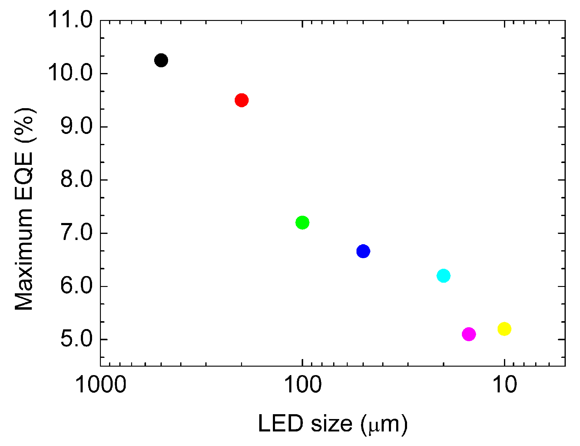
Reduction in the size of micro-LEDs and spacing between devices can cause problems in chip processing and deteriorate LED performance. One important problem is the degradation of the quantum efficiency and homogeneity due to sidewall effect related to high density of surface defects caused during device processing, which leads to degraded electrical injection in the p-GaN [5,30]. Acting as non-radiative centers, the surface defects on the sidewalls significantly degrade the internal quantum efficiency of the micro-LEDs. A decrease in maximum external quantum efficiency (EQE) from ~10% to ~5% with reduction in chip size from above 500 μm × 500 μm to 10 μm × 10 μm has been reported for micro-LEDs, as shown in Figure 2 [31]. The effect of size-reduction on the performances is more noticeable for smaller LEDs with larger perimeter-to-area ratios. For LEDs with the smallest dimensions (below 5 μm), the peak quantum efficiency was reported to be below 10% or even 1% [19]. Therefore, processing technologies to minimize sidewall damage and avoid, if not totally eliminate, degradation of electrical injection are needed. Chen et al. have reported that in pyramidal micro-LEDs, a SiO2 leakage current confinement layer can decrease the reverse leakage current by two orders of magnitude, and the light output of the micro-LEDs can be improved by 115% averagely [32]. Wong et al. have demonstrated that using atomic-layer deposition (ALD) of SiO2 for sidewall passivation, size-dependent factors on peak EQE of micro-LEDs can be minimized [33]. Enhancement in light extraction and reduction in leakage current caused by surface recombination and sidewall damage led to an EQE of 33% for 20 μm × 20 μm micro-LEDs with ALD passivation, compared to 24% without sidewall passivation. Be changing mesa etching process formation between p-contact and hybridization pads into a softer plasma and changing p-contact metal from Ni-based to Ag-based, Olivier et al. have improved the EQE of 10 μm pixel pitch micro-LEDs from 4.8% to 6.8%, and achieved a brightness of 107 cd/m² [5]. Hwang et al. have reported that high EQEs may be maintained when decreasing the chip size from 100 μm × 100 μm to 10 μm × 10 μm, with peak EQEs of 48.6 and 40.2%, respectively [30].
3. Assembly Technologies
Two different approaches have been utilized to assemble displays constructed from individual micro-LED dies. The first one is based on mass transfer, i.e., the so called pick-and-place approach, which includes picking up each individual micro-LED, and precisely positioning it onto the backplane, followed electrically connecting it to the driver IC. This approach allows realization of LED displays in which the active LED area occupies only a small portion of the total area. It can be used for building large-size displays ranging from several inches to tens of inches (such as TV, smartphones, and tablets), which are referred to as direct-view displays [34]. Alternatively, to avoid the complicated pick-and-place mass transfer process, a variety of monolithic fabrication methods have been proposed in order to realize micro-LED displays. Due to the limitation in wafer size used for the growth of LEDs, the monolithic integration approach can only be used for building relatively small-size displays such as near-to-eye projectors and smart watches, which are referred to as micro-LED micro-displays [34].
3.1. Mass Transfer Technologies
Traditional pick and place equipment via mechanical manipulation fails to transfer millions of LED dies in a cost-effective manner. In recent years, many companies have devoted considerable effort to overcome this problem by exploring a number of approaches involving of laser, electrostatic, or electromagnetic, van der Waals forces, or fluidic forces, as summarized in Table 1.
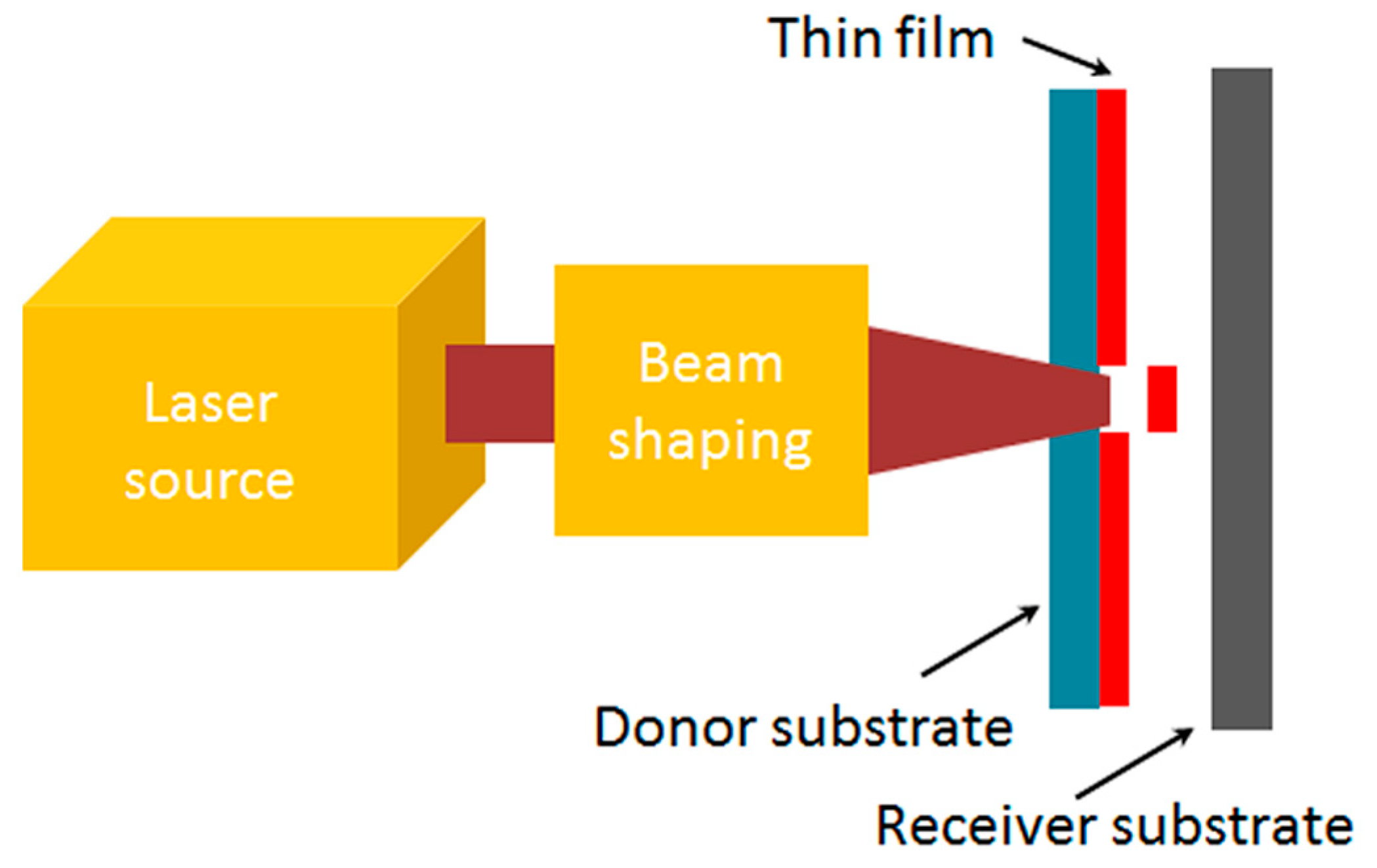
Laser-induced forward transfer is a mass transfer process which uses a laser beam to induce the separation of the micro-LEDs from their carrier substrate and then transfer them to a receive substrate, as shown in Figure 3 [35]. The irradiation with a laser beam results in the light-matter interaction at the interface between the carrier substrate and the dies, with the result that the dies are detached from the substrate and, at the same time, generates a local mechanical force to push the dies toward the receive substrate. The interfacial interaction can be the same as that used in laser lift-off process of GaN LEDs from the sapphire substrate, in which a thin GaN layer (~10 nm) is ablated at the substrate epi interface and decomposed into nitrogen gas and liquid Ga. It may also be implemented via using a temporary substrate with a polymer adhesive serving as the interfacial layer, which decomposes when irradiated with a laser beam. It has been reported that the Laser-induced forward transfer technology enables some 1000 chips to be transferred per laser shot. Optovate, a British optic tech company, has demonstrated its patterned laser lift-off (p-LLO) transfer technology to transfer blue micro-LEDs from a sapphire wafer to a receive substrate. Val R. Marinov has reported that a transfer rate above 100 million per hour can be achieved using the massively parallel laser-enabled transfer (MPLET) technology [36].
Fluidic assembly via gravity and capillary forces to drive and capture the micro-LEDs on to the array of the driver ICs has also been investigated for mass transfer of LED chips [37,38]. The self-assembly is conducted in a fluid, such as isopropanol, acetone or distilled water. The fluid suspends and lets the LEDs move across the surface of the receive substrate till they reach the open receptor sites where they are captured. Once positioned, the anode and cathode electrodes of the micro-LEDs can then be bonded with the driver ICs for electrical connections. eLux, a Foxconn-owned company, has been developing its fluidic assembly methods for massive parallel assembly of micro-LEDs [39]. It was reported that a fill (transfer) rate over 50 million devices per hour can be achieved.
LuxVue, an Apple Co.-owned company, has developed a transfer technology that operates in accordance with the electrostatic principle, which uses the attraction of opposite charges to pick up micro-LEDs [40]. The process consists of picking up an array of micro-LEDs from a carrier substrate with an array of electrostatic transfer heads, which is applied with a pull-in voltage from the working circuitry to generate a grip pressure, contacting the micro-LEDs and transferring heat from the head and liquefying the bonding layer on the receive substrate, and bonding the array to the receiving substrate and finally release the micro-LEDs.
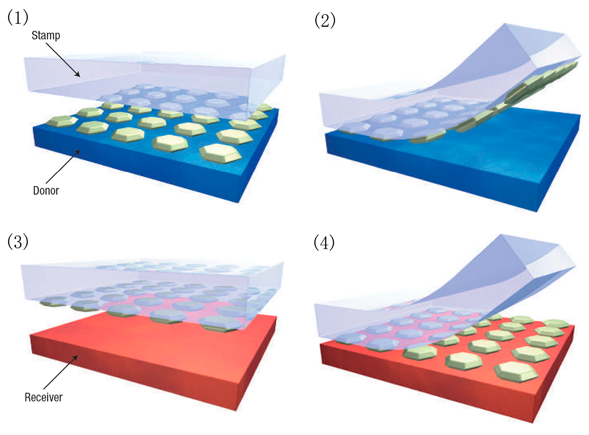
X-Celeprint has developed an elastomer stamp micro-assembly technology for mass transfer of micro-LEDs, as shown in Figure 4 [41]. The process starts with preparation of a native wafer substrate that supports the fully formed, organized arrays of micro-LEDs. Then a soft elastomeric stamp is brought into contact with the micro-LEDs. With a sufficiently high peel velocity, the micro-LEDs are attached on to the stamp and lifted away from the native substrate due to the rate-dependent adhesion forces, which are dominated by van der Waals interactions. Then, with a sufficiently low peel velocity, the micro-LEDs are released from the stamp and preferentially adhered to the receiving substrate.
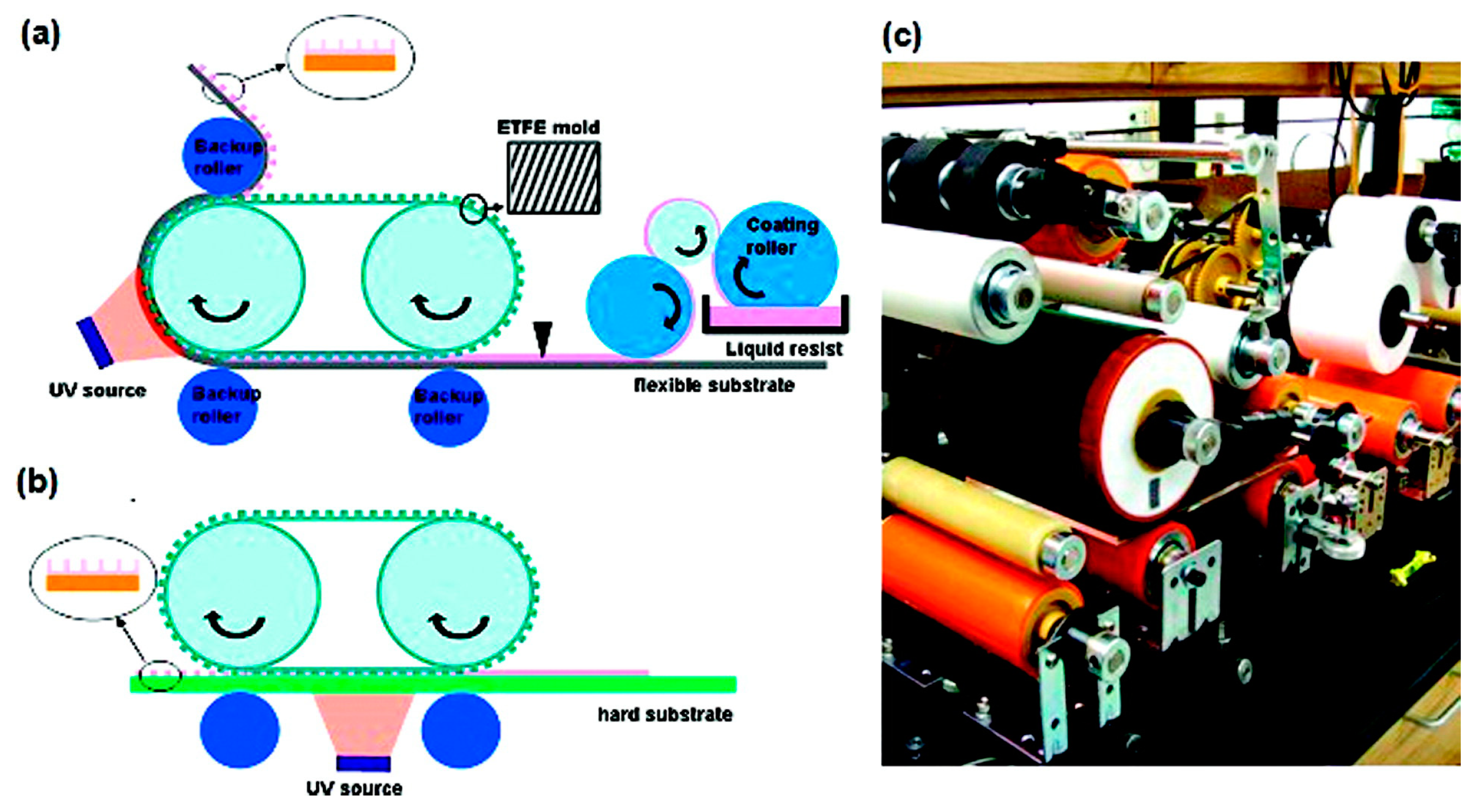
In another approach, a roll-to-plate transfer process has been developed by the Korean Institute of Machinery and Materials (KIMM) [42,43], which can be used to transfer micro-LEDs with a chip size and a chip thickness below 100 µm and 10 µm, respectively, as shown in Figure 5. The process can provide a transfer rate of up to 10,000 devices per second for flexible, stretchable and lightweight displays. The whole process consists of three roll transfer steps. The first step is to pick up and place the array of control TFTs on to a temporary substrate by roll stamp coated with disposable transfer film. Then in the second step, micro-LEDs are lifted off from their support substrate to be located onto the temporary substrate and connected with the TFTs by solder bonding. In the final step, the array of the interconnected micro-LED+TFTs is roll-transferred onto a target substrate to form an active matrix micro-LED display.
3.2. Monolithic Fabrication of Micro-Displays
Simply, the monolithic methods can be divided into two categories, i.e., fully monolithic integration and monolithic hybrid. In conventional display technologies, such as LCDs or OLEDs, the processing temperatures for the emission elements are typically below 400 °C, which can be withstood by the CMOS-based driver ICs. Therefore, fully monolithic integration via direct process of emission elements on the driver ICs is not problematic. However, the growth temperatures of III-nitride LEDs are typically above 900 °C. It is impossible to grow and process LEDs directly on top of backplane with conventional ICs. Additionally, some new fully monolithic methods have been proposed and investigated.
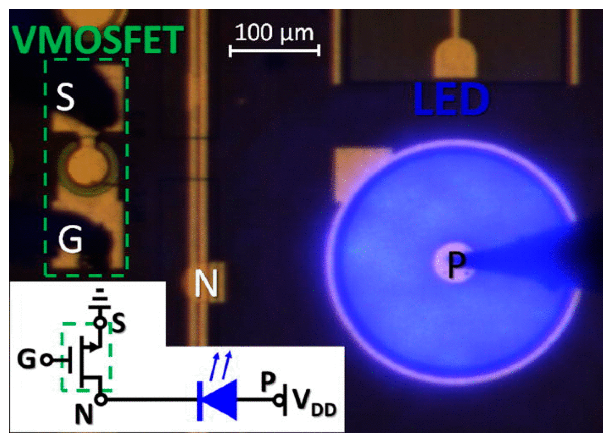
Since III-nitrides are excellent materials for both LEDs and high-frequency and high-power transistors, fully monolithic active matrix micro-displays can be realized by the integration of individual GaN-based LED driven by a GaN-based transistor for each pixel. Lau et al. have reported monolithic integration of InGaN/GaN light emitting diodes (LEDs) with AlGaN/GaN heterojunction field effect transistors (HFETs) [44] or vertical metal-oxide-semiconductor field effect transistor (VMOSFET) drivers [45], by selective growth of HFET or VMOSFET structures on the LED epilayers, as shown in Figure 6. Alternatively, lateral integration via selective removal of the HFET structure followed by selective growth of the LED structure on top of the exposed GaN buffer layer [46] or selective removal of the LED structure followed by selective growth of the metal-oxide-semiconductor field effect transistor (MOSFET) on top of the exposed n-GaN layer [47] have also been reported. Although it has been demonstrated that the performance of the integrated single LED-transistor chip is comparable to discrete LEDs and transistors [44] fabrication of micro-LED displays using this approach has not yet been reported.
Si-based TFT, instead of III-nitride-based transistor, has also been investigated for on-chip driving III-nitride LEDs. Tsuchiyama et al. have reported monolithic integration of a Si n-MOSFET and a GaN micro-LED [48,49]. To achieve this, a Si layer from a silicon-on-insulator (SOI) substrate was bonded to a GaN-based LED structure with a top SiO2 layer via surface-activated bonding [44]. Si-MOSFETs were then fabricated on the Si/SiO2/GaN-LED structure by using a CMOS process line. The interconnects were realized via the connection of the cathode of a 30 × 30 μm2 sized GaN-LED to the drain of a Si n-MOSFET with a gate width of 100 μm and gate length of 10 μm. It was found that thermal degradation could be avoided by optimizing the thickness of the top-Si layer coupled with processing below 900 °C. It is stated that electrical and optical properties of the integrated Si n-MOSFET and GaN micro-LED devices are comparable to those of the standard devices.
Due to the difficulties and incompatibility between the micro-LED and driver IC processes in fully monolithic integration, the most common approach adopted by micro-LED display developers is monolithic hybrid. This approach comprises fabrication of III-nitride based micro-LED arrays, manufacturing of Si-based CMOS driver matrix, and then their hybrid integration in order to allow control of the LED pixels individually. The hybridization process is generally based on the flip-chip bonding technology, which has been widely developed in III-V/Si photonics for high-performance switching and computing [50]. For example, by using 6 μm-sized indium metal bumps deposited on micro-LED pixels as bonders, Day et al. have demonstrated fabrication of a 160 × 120 VGA micro-display with a pixel pitch of 15 μm [51].
To further shrink the pixel pitch down to below 10 μm for higher resolution, CEA-Leti has developed a micro-tube technology to perform the integration process [52,53]. The key step to the interconnection is the insertion of gold capped micro-tubes on the pads of Si circuit into the soft indium pads on the micro-LED array, with the micro-tubes created by using conformal metal deposition and “gap fill” type processes. Blue and green active-matrix LED micro-displays with a 10 μm pixel pitch and a resolution of 873 × 500 using 6 μm-sized micro-LEDs have been demonstrated via this technology.
In addition to the abovementioned monolithic fabrication approaches, it has also been demonstrated that micro-LEDs displays can be built by using GaN-based nanowire LEDs, without the need of mass transfer. Prototypes including a 1.5” 264 PPI RGB wearable display using 20 μm-sized micro-LEDs on a LTPS glass backplane, and a 0.7” 1000 PPI RGB display using 10 μm-sized micro-LEDs on a CMOS backplane have been unveiled by glō-USA, in which direct wafer-to-wafer transfer technology was employed.
4. Full-Color Schemes
As for most micro-display applications, full-colors (composed of the three primary colors red, green, and blue) are needed for each pixel. The widespread display technology LCD is based on light generated by an LED backlight and passing through a matrix of liquid crystal “light switches” and color filters constituting the individual subpixel. While micro-LED display is based on a matrix of tiny light emitters made of micro-LEDs for each subpixel in which brightness can be individually controlled. However, III-nitride LEDs, similar to other heterojunction-based semiconductor structures, are nearly monochromatic emission sources, emitting light at a single color, with its wavelength determined mainly by the indium content in the InGaN/GaN multiple quantum wells (MQWs). Although several approaches exist to produce full-color micro-displays from single color micro-LEDs, it remains to be a challenge for developers.
The most straightforward approach for full color is to assemble discrete commercial LEDs with the three different colors to form an array, with each pixel containing red, green, and blue LED dies. In theory, InGaN/GaN MQWs LEDs can generate all these three colors by tuning the indium content in the MQWs. Unfortunately, InGaN-based green and red LEDs still possess a relatively low luminescence efficiency, which partially results from large lattice mismatch between the InGaN active layer and GaN buffer for green and red wavelengths. This limits the progress in developing full-color displays using GaN family alone. GaP/GaAs based LEDs can be used to emit red light, but may suffer from even more significant drop in EQE as the size shrinks [30].
To enhance the color quality, Soitec, a French company, has developed a substrate technology called InGaNOX [54,55]. The initially strained 200 nm thick InGaN layer with indium content from 1.5% to 8% is grown on a GaN/sapphire substrate. Then the thin InGaN layer is transferred using Soitec’s Smart Cut™ technology onto a compliant layer deposited on a substrate. After patterning, the strain-relaxed, Ga-face-exposed InGaN layer with an in-plane lattice parameter ranging from 3.190 to 3.205 Å is transferred to a final handle substrate with sizes up to 300 mm, which can be sapphire, glass, or silicon. By using this technology, InGaN micro-LEDs with full-color emission (without using phosphor conversion) grown on the same wafer have been fabricated. Red LEDs with emission wavelength up to 630 nm and a chip size of 100 × 100 µm2 have been demonstrated by Soitec.
Another approach utilizes single color micro-LED array but with color converters. The color of the pump LEDs in the LED arrays can be blue or ultraviolet (UV), and phosphors or quantum dots (QDs) can be employed as color converters. When blue micro-LED pump is used, only red and green color-converters are needed with blue partially getting through; while the employment of UV micro-LEDs requires blue, red, and green color-converters. One major challenge in obtaining full-color with this method is the precise placement of the color-convertors on to the sub-pixels with a very small size. A variety of technologies can be used to deposit color converters for LED color-conversion, including spin coating, mist coating, pulse-spray coating, stamp printing, ink jet printing, and aerosol jet printing [56,57,58,59]. Among all of these technologies, aerosol jet printing has the advantages of being precise, non-contact, masks-less, and capable of depositing highly viscous inks and depositing more materials in one printing step. Therefore, this method is deemed as a suitable approach for application in color-conversion in high-resolution micro-LED displays.
Phosphors, which are typically micrometer-sized powders, have the advantages of high quantum yield (exceeding 80%), high thermal stability (with temperature up to 150 °C), high chemical stability (moisture resistance), and stable quantum yield and spectral properties under continuous irradiation with high light flux and fast luminescence decay. Consequently, they are widely used in white LEDs for general lighting [60,61,62]. The shortcomings, however, are strong light scattering and poor beam collimation due to their large size [61]. These shortcomings lead to low color uniformity which becomes more pronounced for micro-LED displays in which the phosphor size is comparable to that of small micro-LEDs. Reducing the phosphor size down to the nanometer scale has the potential to enhance luminance homogeneity due to reduced light scattering [63]. However, it also results in a reduction in quantum efficiency.
QDs have been proposed as an alternative method for full-color micro-LED displays due to their excellent properties, which include high quantum efficiency, large absorption cross-section, and tunable emission wavelength [62]. As compared to typical phosphor particles, the size of colloidal QDs lies in the range of nanometers. Therefore, enhanced color uniformity via QDs-based color-conversion can be expected. White light generation and good luminous efficacy of radiation have been demonstrated in 128 × 128 full-color micro-LED arrays with a pixel pitch of 40 μm, by combining UV micro-LEDs with RGB CdSe QDs deposited via aerosol jet printing [56]. For commercialization, some critical factors in QDs, such as photo-stability and thermal quenching, would have to be addressed.
To ensure the color purity and contrast ratio, the optical cross-talk effect resulting from the inaccurate distribution of color converters must be minimized. It has been reported that for a 128 × 128 micro-LED array with 35 μm × 35 μm pixel size, cross-talk resulting from the overflow of QDs during solvent evaporation still caused color shift, even though the aerosol jet printing technique with optimized parameters was employed [64]. To reduce cross talk, Lin et al. have developed a lithographically fabricated photoresist mold consisting of a window for QD jetting and a light blocking wall, as shown in Figure 7 [64]. Using the window-confined photoresist mold led to successful suppression of the overflow of the QDs resulting in a clear boundary between the pixels. With silver coatings on the sidewall of the mold, light leakage was also prevented and, hence, a near zero cross-talk was achieved. In order to increase the utilization of light from UV micro-LED array, and avoid biological damage, a distributed Bragg reflector (DBR) structure has been implemented on the QDs-deposited LED array, which enhanced the QD emission intensity by 23%, 32%, and 5% for red, green, and blue, respectively [64].
In another study, Chen et al. have used three strategies to improve pixel contrast ratio and color purity of monolithic RGB micro-LEDs based on blue LEDs and red and green QDs, which include a black matrix photoresist with light-blocking capability to block light leakage from the sidewalls, a DBR with high reflectivity at blue light on the top of red and green QDs/micro-LEDs and a hybrid Bragg reflector (HBR) structure on the bottom for multiple reflection of the blue light into the color conversion layer [65]. Consequently, the contrast ratio of the micro-LEDs was improved from 11 to 22, and the red and green light output intensities of the micro LEDs were enhanced by about 27%.
To improve light efficiency and eliminate color crosstalk of color-converted micro-LED displays, Gou et al. have proposed a funnel-tube array design in color-converted micro-LED displays with color filter [66]. Based on device simulation and modeling, it was found that by using funnel-tube array to confine phosphors inside each subpixel, the optical efficiency of the micro-LED display can be improved by ~3 times, while the crosstalk is eliminated. With optimized tapper angle of the funnel-tube, the ambient contrast ratio can also be improved due to higher light intensity.
5. Current Challenges and Prospects
Despite the above-discussed technological advancements, there are still some remaining critical bottlenecks which need to be overcome for high volume manufacturing of micro-LED displays. The major one is the pixel yield of the display. To control the dead pixel number less than 5 in an RGB full-color full high definition (FHD) display (1920 × 1080 pixels), the yield should be 99.9999%, which is too high for today’s achievable level. A dead pixel can appear at different stages of the fabrication, such as epitaxy, LED chip process, transfer process. For example, in the case of monolithic fabrication, in a passive-matrix micro-LED array fabricated by flip-chip bonding of a GaN micro-LED array on a silicon submount with common p-electrode stripes, numerous dead pixels are formed because of physical disconnection from the p-electrode line caused by severe bonding failures [67]. As another example, the photoresist residue inside the gaps between the LED elements can greatly undermine the yield of the display [29]. Without adding an O2-based plasma ashing step, for the arrays with 170 μm gaps between mesas, the micro-LED element yield in the array is approximately 90%. However, when the gap width is reduced to 6 μm, the yield drops to around 67%. Introduction of the ashing step to remove the photoresist residues improved the yield to 100% and over 95% for the 170 μm and 6 μm gap arrays, respectively.
Another challenge is the defect management and repair technology. For a zero dead defect display, even assuming an extremely high yield, a repair process is unavoidable. A straightforward solution is to increase the redundancy by doubling the number of micro-LED element for each pixel. However, the effectiveness of the built-in redundancy depends on the initial defectivity yield. If the yield is 99.99%, doubling the number of micro-LED can reduce the number of dead pixels from 5000 to five pixels in an FHD display. However, if the yield is only 99.9%, the number of dead pixels would be still 500 [68]. Since doubled, number-wise, micro-LEDs are used, the cost of the display would be greatly increased. Alternatively, some developers have proposed individual pixel repair technologies. Unfortunately, this approach is also costly, and cannot be applied for displays produced by monolithic fabrication.
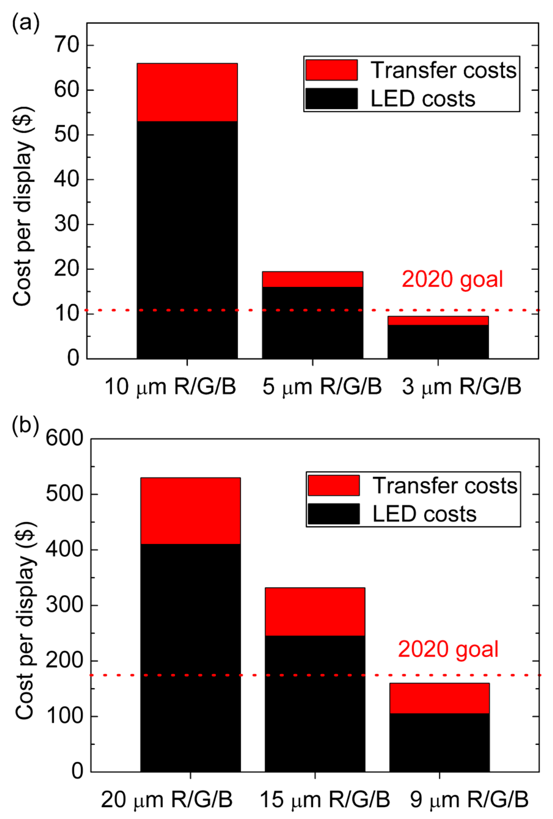
The cost remains to be a formidable obstacle. The success of micro-LED display insertion hinges on its cost competitiveness against the competing technologies such as the conventional LCD/OLED displays, but at the time of this writing cost competiveness is not yet realistic. The cost of micro-LED displays naturally encompasses wafer and chip processing cost, repair cost, post-processing cost, and transfer cost in the case of pick-and-place approach [69]. Figure 8 shows the calculated LED and mass transfer cost versus micro-LED size for a 5.8” 2560 × 1440 resolution quad high definition (QHD) smartphone display and 3840 × 2160 resolution 4K TV display by IHS Research and Veeco [21]. Based on the assumption of $400 per 6” processed epitaxy wafer and a LED gap of 2 μm, a size of 3 μm × 3 μm and 9 μm × 9 μm is needed for smartphone and TV, respectively, to meet the competitive cost targets with OLED. Continual technology advancements can be expected to provide the pathways to realize the cost expectation, but more time is needed to be in a position for us to select which of the strategies touched upon in this paper would get the technology of choice where it needs to be.
Despite the bottlenecks, developers, motivated by the great potential, remain quite optimistic about the potential of micro-LED displays. It is anticipated that high volume commercialization of micro-LED displays could become true in the coming years 2019–2020, with the first insertion being by small-size devices, such as head up displays (HUD), wearables and also low pixel per inch (PPI) displays such as video walls, according to the Yole Développement’s estimation [19].
Author Contributions
All the authors have participated in the literature review and in the correction and revision of the manuscript.
Conflicts of Interest
The authors declare no conflict of interest.
References
- Jiang, H.X.; Lin, J.Y. Nitride micro-LEDs and beyond—A decade progress review. Opt. Express 2013, 21, A475. [Google Scholar] [CrossRef] [PubMed]
- Fan, J.Y.; Lin, J.Y.; Jiang, H.X. III-nitride micro-emitter arrays: Development and applications. J. Phys. D Appl. Phys. 2008, 41, 094001. [Google Scholar] [CrossRef]
- Dupré, L.; Marra, M.; Verney, V.; Aventurier, B.; Henry, F.; Olivier, F.; Tirano, S.; Daami, A.; Templier, F. Processing and characterization of high resolution GaN/InGaN LED arrays at 10 micron pitch for micro display applications. In Proceedings of the SPIE, Warsaw, Poland, 4–8 July 2017; Volume 10104. [Google Scholar]
- Radauscher, E.J.; Meitl, M.; Prevatte, C.; Bonafede, S.; Rotzoll, R.; Gomez, D.; Moore, T.; Raymond, B.; Cok, R.; Fecioru, A. Miniaturized LEDs for flat-panel displays. In Proceedings of the SPIE, San Francisco, CA, USA, 30 January–1 February 2017; Volume 10124, p. 1012418. [Google Scholar]
- Olivier, F.; Daami, A.; Dupré, L.; Henry, F.; Aventurier, B.; Templier, F. 25-4: Investigation and improvement of 10 μm Pixelpitch GaN-based Micro-LED arrays with very high brightness. SID Int. Symp. Dig. Tech. Pap. 2017, 48, 353. [Google Scholar] [CrossRef]
- Poher, V.; Grossman, N.; Kennedy, G.T.; Nikolic, K.; Zhang, H.X.; Gong, Z.; Drakakis, E.M.; Gu, E.; Dawson, M.D.; French, P.M.W. Micro-LED arrays: A tool for two-dimensional neuron stimulation. J. Phys. D Appl. Phys. 2008, 41, 094014. [Google Scholar] [CrossRef]
- Grossman, N.; Poher, V.; Grubb, M.S.; Kennedy, G.T.; Nikolic, K.; McGovern, B.; Berlinguer Palmini, R.; Gong, Z.; Drakakis, E.M.; Neil, M.A.; et al. Multi-site optical excitation using ChR2 and micro-LED array. J. Neural Eng. 2010, 7, 016004. [Google Scholar] [CrossRef]
- Zarowna-Dabrowska, A.; Neale, S.L.; Massoubre, D.; McKendry, J.; Rae, B.R.; Henderson, R.K.; Rose, M.J.; Yin, H.; Cooper, J.M.; Gu, E. Miniaturized optoelectronic tweezers controlled by GaN micro-pixel light emitting diode arrays. Opt. Express 2011, 19, 2720. [Google Scholar] [CrossRef] [Green Version]
- Goßler, C.; Bierbrauer, C.; Moser, R.; Kunzer, M.; Holc, K.; Pletschen, W.; Köhler, K.; Wagner, J.; Schwaerzle, M.; Ruther, P. GaN-based micro-LED arrays on flexible substrates for optical cochlear implants. J. Phys. D Appl. Phys. 2014, 47, 205401. [Google Scholar] [CrossRef]
- Guilhabert, B.; Massoubre, D.; Richardson, E.; McKendry, J.J.D.; Valentine, G.; Henderson, R.K.; Watson, I.M.; Gu, E.; Dawson, M.D. Sub-micron lithography using InGaN micro-LEDs: mask-free fabrication of LED arrays. IEEE Photonics Technol. Lett. 2012, 24, 2221–2224. [Google Scholar] [CrossRef]
- Zhao, L.; Zhu, S.; Wu, C.; Yang, C.; Yu, Z.; Yang, H.; Liu, L. GaN-based LEDs for light communication. Sci. China Phys. Mech. Astron. 2016, 59, 107301. [Google Scholar] [CrossRef]
- Chun, H.; Rajbhandari, S.; Faulkner, G.; Tsonev, D.; Xie, E.; James, J.; McKendry, D.; Gu, E.; Dawson, M.D.; O’Brien, D.C.; et al. LED based wavelength division multiplexed 10 Gb/s visible light communications. Lightwave Technol. 2016, 34, 3047–3052. [Google Scholar] [CrossRef]
- McKendry, J.J.D.; Green, R.P.; Kelly, A.E.; Gong, Z.; Guilhabert, B.; Massoubre, D.; Gu, E.; Dawson, M.D. High-speed visible light communications using individual pixels in a micro light-emitting diode array. IEEE Photonics Technol. Lett. 2010, 22, 1346–1348. [Google Scholar] [CrossRef]
- Rajbhandari, S.; McKendry, J.J.D.; Herrnsdorf, J.; Chun, H.; Faulkner, G.; Haas, H.; Watson, I.M.; O’Brien, D.; Dawson, M.D. A review of gallium nitride LEDs for multi-gigabit-per-second visible light data communications. Semicon. Sci. Technol. 2017, 32, 023001. [Google Scholar] [CrossRef]
- Konoplev, S.S.; Bulashevich, K.A.; Karpov, S.Y. From Large-Size to Micro-LEDs: Scaling Trends Revealed by Modeling. Phys. Stat. Sol. A 2018, 215, 1700508. [Google Scholar] [CrossRef]
- Choi, H.W.; Jeon, C.W.; Dawson, M.D.; Edwards, P.R.; Martin, R.W.; Tripathy, S. Mechanism of enhanced light output efficiency in InGaN-based microlight emitting diodes. J. Appl. Phys. 2003, 93, 5978–5982. [Google Scholar] [CrossRef] [Green Version]
- Thibeault, B.; DenBaars, S. Enhanced light extraction through the use of micro-LED arrays. Patent No. 6,410,942, 25 June 2002. [Google Scholar]
- Adivarahan, V.; Wu, S.; Sun, W.H.; Mandavilli, V.; Shatalov, M.S.; Simin, G.; Yang, J.W.; Maruska, H.P.; Asif Khan, M. High-power deep ultraviolet light-emitting diodes basedon a micro-pixel design. Appl. Phys. Lett. 2004, 85, 1838–1840. [Google Scholar] [CrossRef]
- Virey, E.H.; Baron, N. Status and Prospects of microLED Displays. SID Int. Symp. Dig. Tech. Pap. 2018, 49, 593–596. [Google Scholar] [CrossRef]
- Beckers, A.; Fahle, D.; Mauder, C.; Kruecken, T.; Boyd, A.R.; Heuken, M. Enabling the Next Era of Display Technologies by Micro LED MOCVD Processing. SID Int. Symp. Dig. Tech. Pap. 2018, 49, 601–603. [Google Scholar] [CrossRef]
- Paranjpe, A.; Montgomery, J.; Lee, S.M.; Morath, C. Micro-LED Displays: Key Manufacturing Challenges and Solutions. SID Int. Symp. Dig. Tech. Pap. 2018, 49, 597–600. [Google Scholar] [CrossRef]
- Amour, E.; Lu, F.; Belousov, M.; Lee, D.; Quinn, W. LED growth compatibility between 2”, 4” and 6” sapphire. Semicond. Today 2009, 4, 82–86. [Google Scholar]
- Lu, F.; Lee, D.; Byrnes, D.; Armour, E.; Quinn, W. Blue LED growth from 2 inch to 8 inch. Sci. China Technol. Sci. 2011, 54, 33–37. [Google Scholar] [CrossRef]
- Aida, H.; Lee, D.S.; Belousov, M.; Sunakawa, K. Effect of Initial Bow of Sapphire Substrate on Substrate Curvature during InGaN Growth Stage of Light Emitting Diode Epitaxy. Jpn. J. Appl. Phys. 2012, 51, 012102. [Google Scholar] [CrossRef]
- Aida, H.; Aota, N.; Takeda, H.; Koyama, K. Control of initial bow of sapphire substrates for III-nitride epitaxy by internally focused laser processing. J. Cryst. Growth 2012, 361, 135–141. [Google Scholar] [CrossRef]
- Hoffmann, V.; Knauer, A.; Brunner, C.; Einfeldt, S.; Weyers, M.; Tränkle, G.; Haberland, K.; Zettler, J.T.; Kneissl, M. Uniformity of the wafer surface temperature during MOVPE growth of GaN-based laser diode structures on GaN and sapphire substrate. J. Cryst. Growth 2011, 315, 5–9. [Google Scholar] [CrossRef]
- Aida, H.; Takeda, H.; Aota, N.; Koyama, K. Reduction of bowing in GaN-on-sapphire and GaN-on-silicon substrates by stress implantation by internally focused laser processing. Jpn. J. Appl. Phys. 2011, 51, 016504. [Google Scholar] [CrossRef]
- Liu, Z.J.; Chong, W.C.; Wong, K.M.; Keung, C.W.; Lau, K.M. Investigation of Forward Voltage Uniformity in Monolithic Light-Emitting Diode Arrays. IEEE Photonics Technol. Lett. 2013, 25, 1290–1293. [Google Scholar] [CrossRef]
- Xie, E.; Stonehouse, M.; Ferreira, R.; Jonathan, J.; McKendry, D.; Herrnsdorf, J.; He, X.; Rajbhandari, S.; Chun, H.; Aravind, V.; et al. Design, Fabrication, and Application of GaN-Based Micro-LED Arrays With Individual Addressing by N-Electrodes. IEEE Photonics J. 2017, 9, 7907811. [Google Scholar] [CrossRef]
- Hwang, D.; Mughal, A.; Pynn, C.D.; Nakamura, S.; DenBaars, S.P. Sustained high external quantum efficiency in ultrasmall blue III–nitride micro-LEDs. Appl. Phys. Express 2017, 10, 032101. [Google Scholar] [CrossRef]
- Olivier, F.; Tirano, S.; Dupré, L.; Aventurier, B.; Largeron, C.; Templier, F. Influence of size-reduction on the performances of GaN-based micro-LEDs for display application. J. Lumin. 2017, 191, 112–116. [Google Scholar] [CrossRef]
- Chen, W.; Hu, G.; Lin, J.; Jiang, J.; Liu, M.; Yang, Y.; Hu, G.; Lin, Z.; Wu, Z.; Liu, Y. High-performance, single-pyramid micro light-emitting diode with leakage current confinement layer. Appl. Phys. Express 2015, 8, 032102. [Google Scholar] [CrossRef]
- Wong, M.S.; Hwang, D.; Alhassan, A.I.; Lee, C.; Ley, R.; Nakamura, S.; DenBaars, S.P. High efficiency of III-nitride micro-light-emitting diodes by sidewall passivation using atomic layer deposition. Opt. Express 2018, 26, 21324–21331. [Google Scholar] [CrossRef]
- Lee, V.W.; Twu, N.; Kymissis, I. Frontline technology micro-LED technologies and applications. Inf. Disp. 2016, 32, 16–23. [Google Scholar]
- Delaporte, P.; Alloncle, A.-P. Laser-induced forward transfer: A high resolution additive manufacturing technology. Opt. Laser Technol. 2016, 78, 33–41. [Google Scholar] [CrossRef]
- Marinov, V.R. Laser-Enabled Extremely-High Rate Technology for µLED Assembly. SID Int. Symp. Dig. Tech. Pap. 2018, 49, 692–695. [Google Scholar] [CrossRef]
- Yeh, H.-J.J.; Smith, J.S. Fluidic self-assembly for the integration of GaAs light-emitting diodes on Si substrates. IEEE Photonics Technol. Lett. 1994, 6, 706–708. [Google Scholar] [CrossRef]
- Saeedi, E.; Kim, S.S.; Parviz, B.A. Self-assembled inorganic micro-display on plastic. In Proceedings of the 2007 IEEE 20th International Conference on Micro Electro Mechanical Systems (MEMS), Hyogo, Japan, 21–25 January 2007. [Google Scholar]
- Schuele, P.J.; Sasaki, K.; Ulmer, K.; Lee, J.-J. Display with surface mount emissive elements. Patent No. 9,825,202, 11 May 2017. [Google Scholar]
- Bibl, A.; Higginson, J.A.; Hu, H.-H.; Law, H.-F.S. Method of transferring and bonding an array of micro devices. Patent No. 9,773,750, 26 September 2017. [Google Scholar]
- Meitl, M.A.; Zhu, Z.-T.; Kumar, V.; Lee, K.J.; Feng, X.; Huang, Y.Y.; Adesida, I.; Nuzzo, R.G.; Rogers, J.A. Transfer printing by kinetic control of adhesion to an elastomeric stamp. Nat. Mater. 2006, 5, 33. [Google Scholar] [CrossRef]
- Ahn, S.H.; Guo, L.J. Large-area roll-to-roll and roll-to-plate nanoimprint lithography: a step toward high-throughput application of continuous nanoimprinting. ACS Nano 2009, 3, 2304–2310. [Google Scholar] [CrossRef]
- Sharma, B.K.; Jang, B.; Lee, J.E.; Bae, S.-H.; Kim, T.W.; Lee, H.-J.; Kim, J.-H.; Ahn, J.-H. Load-Controlled Roll Transfer of Oxide Transistors for Stretchable Electronics. Adv. Funct. Mater. 2013, 23, 2024–2032. [Google Scholar] [CrossRef]
- Liu, Z.J.; Huang, T.; Ma, J.; Liu, C.; Lau, K.M. Monolithic integration of AlGaN/GaN HEMT on LED by MOCVD. IEEE Electron. Dev. Lett. 2014, 35, 330–332. [Google Scholar] [CrossRef]
- Lu, X.; Liu, C.; Jiang, H.; Zou, X.; Zhang, A.; Lau, K.M. Monolithic integration of enhancement-mode vertical driving transistorson a standard InGaN/GaN light emitting diode structure. Appl. Phys. Lett. 2016, 109, 053504. [Google Scholar] [CrossRef]
- Liu, C.; Cai, Y.; Zou, X.; Lau, K.M. Low-leakage high-breakdown laterally integrated HEMT-LED via n-GaN electrode. IEEE Photonics Technol. Lett. 2016, 28, 1130–1133. [Google Scholar] [CrossRef]
- Lee, Y.-J.; Yang, Z.-P.; Chen, P.-G.; Hsieh, Y.-A.; Yao, Y.-C.; Liao, M.-H.; Lee, M.-H.; Wang, M.-T.; Hwang, J.-M. Monolithic integration of GaN-based light-emitting diodes and metal-oxide-semiconductor field-effect transistors. Opt. Express 2014, 22, A1589–A1595. [Google Scholar] [CrossRef]
- Tsuchiyama, K.; Yamane, K.; Sekiguchi, H.; Okada, H.; Wakahara, A. Fabrication of Si/SiO2/GaN structure by surface-activated bonding for monolithic integration of optoelectronic devices. Jpn. J. Appl. Phys. 2016, 55, 05FL01. [Google Scholar] [CrossRef]
- Tsuchiyama, K.; Yamane, K.; Utsunomiya, S.; Sekiguchi, H.; Okada, H.; Wakahara, A. Monolithic integration of Si-MOSFET and GaN-LED using Si/SiO2/GaN-LED wafer. Appl. Phys. Express 2016, 9, 104101. [Google Scholar] [CrossRef]
- Lau, K.M.; Keung, C.W.; Liu, Z. Method for manufacturing a monolithic LED micro-display on an active matrix panel using flip-chip technology and display apparatus having the monolithic LED micro-display. Patent No. 8,557,616, 15 October 2013. [Google Scholar]
- Day, J.; Li, J.; Lie, D.Y.C.; Bradford, C.; Lin, J.Y.; Jiang, H.X. III-Nitride full-scale high-resolution microdisplays. Appl. Phys. Lett. 2011, 99, 031116. [Google Scholar] [CrossRef]
- Marion, F.; Bisotto, S.; Berger, F.; Gueugnot, A.; Mathieu, L.; Henry, D.; Templier, F.; Catelain, T. A room temperature flip-chip technology for high pixel count micro-displays and imaging arrays. In Proceedings of the IEEE 66th Electronic Components and Technology Conference (ECTC), Las Vegas, NV, USA, 31 May–3 June 2016. [Google Scholar]
- Templier, F.; Dupré, L.; Dupont, B.; Daami, A.; Aventurier, B.; Henry, F.; Sarrasin, D.; Renet, S.; Berger, F.; Olivier, F. High-resolution active-matrix 10-μm pixel-pitch GaN LED microdisplays for augmented reality applications. In Proceedings of the SPIE 10556, Strasbourg, France, 22–26 April 2018; p. 105560I. [Google Scholar]
- Even, A.; Laval, G.; Ledoux, O.; Ferret, P.; Sotta, D.; Guiot, E.; Levy, F.; Robin, I.C.; Dussaigne, A. Enhanced In incorporation in full InGaN heterostructure grown on relaxed InGaN pseudo-substrate. Appl. Phys. Lett. 2017, 110, 262103. [Google Scholar] [CrossRef]
- Even, A. In incorporation Improvement in InGaN Based Active Region Using InGaN Pseudo Substrate for Monolithic White LED Application; Université Grenoble Alpes: Saint-Martin-d’Hères, France, 2018. [Google Scholar]
- Han, H.-W.; Lin, H.-Y.; Lin, C.-C.; Chong, W.-C.; Li, J.-R.; Chen, K.-J.; Yu, P.; Chen, T.-M.; Chen, H.-M.; Lau, K.-M. Resonant-enhanced full-color emission of quantum-dot-based micro LED display technology. Opt. Express 2015, 23, 32504–32515. [Google Scholar] [CrossRef]
- Rudorfer, A.; Tscherner, M.; Palfinger, C.; Reil, F.; Hartmann, P.; Seferis, I.E.; Zych, E.; Wenzl, F.P. A study on Aerosol jet printing technology in LED module manufacturing. In Proceedings of the SPIE 9954, San Diego, CA, USA, 7 September 2016; p. 99540E. [Google Scholar]
- Singh, M.; Haverinen, H.M.; Dhagat, P.; Jabbour, G.E. Inkjet printing-process and its applications. Adv. Mater. 2010, 22, 673–685. [Google Scholar] [CrossRef]
- Chen, K.-J.; Chen, H.-C.; Tsai, K.-A.; Lin, C.-C.; Tsai, H.-H.; Chien, S.-H.; Cheng, B.-S.; Hsu, Y.-J.; Shih, M.-H.; Tsai, C.-H. Resonant-enhanced full-color emission of quantum-dot-based display technology using a pulsed spray method. Adv. Funct. Mater. 2012, 22, 5138–5143. [Google Scholar] [CrossRef]
- Han, J.K.; Choi, J.I.; Piquette, A.; Hannah, M.; Anc, M.; Galvez, M.; Talbot, J.B.; McKittrick, J. Phosphor development and integration for near-UV LED solid state lighting. ECS J. Solid State Sci. Technol. 2013, 2, R3138. [Google Scholar] [CrossRef]
- Chen, D.-C.; Liu, Z.-G.; Deng, Z.-H.; Wang, C.; Cao, J.-G.; Liu, Q.-L. Optimization of light efficacy and angular color uniformity by hybrid phosphor particle size for white light-emitting diode. Rare Met. 2014, 33, 348–352. [Google Scholar] [CrossRef]
- Xie, B.; Hu, R.; Luo, X.J. Quantum dots-converted light-emitting diodes packaging for lighting and display: status and perspectives. Electron. Packag. 2016, 138, 020803. [Google Scholar] [CrossRef]
- McKittrick, J.; Shea-Rohwer, L.E. Down conversion materials for solid-state lighting. J. Am. Ceram. Soc. 2014, 97, 1327–1352. [Google Scholar] [CrossRef]
- Lin, H.-Y.; Sher, C.-W.; Hsieh, D.-H.; Chen, X.-J.; Chen, H.-M.P.; Chen, T.-M.; Lau, K.-M.; Chen, C.-H.; Lin, C.-C.; Kuo, H.-C. Optical cross-talk reduction in a quantum-dot-based full-color micro-light-emitting-diode display by a lithographic-fabricated photoresist mold. Photonics Res. 2017, 5, 411–416. [Google Scholar] [CrossRef]
- Chen, G.-S.; Wei, B.-Y.; Lee, C.-T.; Lee, H.Y. Monolithic red/green/blue micro-LEDs with HBR and DBR structures. IEEE Photonics Technol. Lett. 2018, 30, 262–265. [Google Scholar] [CrossRef]
- Gou, F.; Hsiang, E.-L.; Tan, G.; Lan, Y.-F.; Tsai, C.-Y.; Wu, S.-T. Tripling the Optical Efficiency of Color-Converted Micro-LED Displays with Funnel-Tube Array. Crystals 2019, 9, 39. [Google Scholar] [CrossRef]
- An, C.-C.; Wu, M.-H.; Huang, Y.-W.; Chen, T.-H.; Chao, C.-H.; Yeh, W.-Y. Study on flip chip assembly of high density micro-LED array. In Proceedings of the 6th International Microsystems, Packaging, Assembly and Circuits Technology Conference (IMPACT), Taipei, Taiwan, 19–21 October 2011; pp. 336–338. [Google Scholar]
- Henry, W.; Percival, C. ILED Displays: Next Generation Display Technology. SID Int. Symp. Dig. Tech. Pap. 2016, 47, 747–750. [Google Scholar] [CrossRef]
- Chaji, R.; Fathi, E.; Zamani, A. Low-Cost Micro-LED Displays for All Applications. SID Int. Symp. Dig. Tech. Pap. 2017, 48, 264–267. [Google Scholar] [CrossRef]
Figure 1.
PL peak wavelength uniformity map for 2, 4, 6, and 8 inch wafers with zero edge exclusion. Their PL uniformity is very comparable, all around 2 nm in standard deviation except the eight inch wafer due to non-optimized wafer pocket design [23]. Reprinted by permission from Springer Nature, Copyright (2011).

Figure 2.
Effect of size-reduction on the maximum EQE of GaN-based micro-LEDs. Data compiled from reference [31].
Figure 2.
Effect of size-reduction on the maximum EQE of GaN-based micro-LEDs. Data compiled from reference [31].

Figure 3.
Schematic of laser-induced forward transfer (LIFT) process. Adapted from reference [35], Copyright 2016, with permission from Elsevier.
Figure 3.
Schematic of laser-induced forward transfer (LIFT) process. Adapted from reference [35], Copyright 2016, with permission from Elsevier.

Figure 4.
Schematic illustration of the generic process flow for elastomer stamp micro-assembly. (1) Prepare donor substrate; apply rubber stamp; (2) quickly peel-back stamp; grab objects off of donor; (3) apply inked stamp to receiving substrate; and (4) slowly peel-back stamp; print objects onto receiver. Reprinted/adapted by permission from Springer Nature: Nature materials, reference [41]. Copyright (2009).

Figure 5.
Schematics of (a) roll-to-roll nanoimprint lithography (R2RNIL) and (b) roll-to-roll nanoimprint lithography (R2PNIL) process. (c) Photograph of a six-inch-capable R2R/R2PNIL apparatus [38]. Copyright 2009 American Chemical Society.
Figure 5.
Schematics of (a) roll-to-roll nanoimprint lithography (R2RNIL) and (b) roll-to-roll nanoimprint lithography (R2PNIL) process. (c) Photograph of a six-inch-capable R2R/R2PNIL apparatus [38]. Copyright 2009 American Chemical Society.

Figure 6.
Optical micrograph of the monolithically integrated VMOSFET-LED device. Reprinted from reference [45], with the permission of AIP Publishing.
Figure 6.
Optical micrograph of the monolithically integrated VMOSFET-LED device. Reprinted from reference [45], with the permission of AIP Publishing.

Figure 7.
Process flow of a full-color microdisplay. (a) The structure of the micro-LED arrays. (b) Aligning the mold to the UV micro-LED array. (c–e) Consequently jetting the RGB QDs inside the mold window to form the full-color pixels. Reprinted from reference [64], with the permission of Chinese Laser Press.

Figure 8.
LED and mass transfer costs versus micro-LED size for 5.8” QHD smartphone (a) and 55” 4K TV (b) by IHS Research and Veeco [21]. Courtesy of Dr. Ajit Paranjpe of Veeco Instruments, Inc.
Figure 8.
LED and mass transfer costs versus micro-LED size for 5.8” QHD smartphone (a) and 55” 4K TV (b) by IHS Research and Veeco [21]. Courtesy of Dr. Ajit Paranjpe of Veeco Instruments, Inc.


Table 1.
Some mass transfer technologies.
| Methods | Company/Institute | Force/means | Transfer rate |
|---|---|---|---|
| Laser lift-off | Optovate/Uniqarta | Laser | 1000 per shot/100 million per hour |
| Fluidic assembly | Foxconn(eLux) | Gravity and capillary | 50 million per hour |
| Electrostatic array | Apple (LuxVue) | Electrostatic | (Not found) |
| elastomer stamp | X-Celeprint | van der Waals | 1 million per hour |
| Roll-to-roll | KIMM | Roll stamp | 10,000 per sec |
© 2019 by the authors. Licensee MDPI, Basel, Switzerland. This article is an open access article distributed under the terms and conditions of the Creative Commons Attribution (CC BY) license (http://creativecommons.org/licenses/by/4.0/).
Share and Cite
MDPI and ACS Style
Ding, K.; Avrutin, V.; Izyumskaya, N.; Özgür, Ü.; Morkoç, H. Micro-LEDs, a Manufacturability Perspective. Appl. Sci. 2019, 9, 1206. https://0-doi-org.brum.beds.ac.uk/10.3390/app9061206
AMA Style
Ding K, Avrutin V, Izyumskaya N, Özgür Ü, Morkoç H. Micro-LEDs, a Manufacturability Perspective. Applied Sciences. 2019; 9(6):1206. https://0-doi-org.brum.beds.ac.uk/10.3390/app9061206
Chicago/Turabian StyleDing, Kai, Vitaliy Avrutin, Natalia Izyumskaya, Ümit Özgür, and Hadis Morkoç. 2019. "Micro-LEDs, a Manufacturability Perspective" Applied Sciences 9, no. 6: 1206. https://0-doi-org.brum.beds.ac.uk/10.3390/app9061206
Note that from the first issue of 2016, this journal uses article numbers instead of page numbers. See further details here.