SVPWM Method for Multilevel Indirect Matrix Converter with Eliminate Common Mode Voltage


Faculty of Electrical and Electronics Engineering, Hochiminh City University of Technology, VNU-HCM, Hochiminh City 70000, Vietnam
*
Author to whom correspondence should be addressed.
Appl. Sci. 2019, 9(7), 1342; https://0-doi-org.brum.beds.ac.uk/10.3390/app9071342
Submission received: 26 February 2019
/
Revised: 19 March 2019
/
Accepted: 25 March 2019
/
Published: 30 March 2019
(This article belongs to the Special Issue Emerging Power Electronics Technologies)
Abstract
:The multilevel indirect matrix converter (IMC) is a merit of power converter for feeding a three-phase load from three-phase power supply because it has several attractive features such as: Sinusoidal input/output currents, bidirectional power flow, long lifetime due to the absence of bulky electrolytic capacitors. As compared to the conventional IMC, the multilevel IMC provides high output performance by increasing the level of output voltage. In this paper, the novel approach topology of multilevel IMC by using the combination of the cascaded rectifier and the three-level T-Type inverter is introduced. Furthermore, the new space vector pulse width modulation (SVPWM) method for the presented multilevel IMC that eliminate the common-mode voltage is proposed in this paper. The simulation study is carried out in PSIM software to verify the proposed modulation method. Then, an experimental system is built using a three-phase RL load, a multilevel IMC, a DSP controller board and other elements to verify the effectiveness of the proposed modulation method. Some simulation and experimental results are illustrated to confirm the theory analysis.
1. Introduction
Recently, the matrix converter (MC) has received considerable attention, especially in applications requiring bi-directional power flow. The MC provides direct AC/AC conversion and it is considered a competitive alternative to the conventional back-to-back converter. Compared to the back-to-back converter, the MC has several attractive features such as the simple and compact power circuit due to the lack of bulky electrolytic capacitors, sinusoidal input and output currents, controllable input power factor with any load, bidirectional power flow capability, long lifetime and high reliability [1,2,3]. Due to these advantages which the MC offers, it attracts many researchers to study and consider it for specialized applications in industry, such as adjustable speed drives, wind generation system, utility supply and ground power supply unit for aircraft servicing [4,5,6,7]. However, MC still has some limitations, e.g., the voltage transfer ratio constraint with a maximum value of 0.866, and a great sensitivity to the power source distortion due to the direct connection between input and output sides. With no intermediate power storage, the ride-through capability of MC is also under consideration of many researchers. And, the complicated commutation is also a shortcoming that makes the MC research more difficult. The MC topologies are divided into two types: Direct matrix converter (DMC) and the indirect matrix converter (IMC). In recent years, the IMC has received an increased amount of interest and has been studied intensely as an alternative to the DMC [8]. The concept of the IMC is to separate the AC/AC converter into two stages, namely, the rectifier stage and inverter stage, without a bulky capacitor. The rectifier stage is comprised of six bidirectional switches while the inverter stage consists of six unidirectional switches as shown in Figure 1.
With the limitation of voltage ratings of power switches and voltage transfer ratio, the conventional IMC is not considered for high-power applications. In last few years, there is growing interest in multilevel MC topologies to extend the application of power converters for higher voltage and power ratio. The multilevel MC can synthesize more than two-level output voltage to improve output performance in terms of reduced harmonic content. The development of multilevel MC is classified on two main topologies, i.e., multilevel direct MC (DMC) [9,10] and multilevel IMC [11,12]. The multilevel IMC provides some advantages which are not available in the DMC, e.g., simple commutation, possibility of reducing number of power switches, and possibility of reconstructing the direct AC/AC with multi three-phase output.
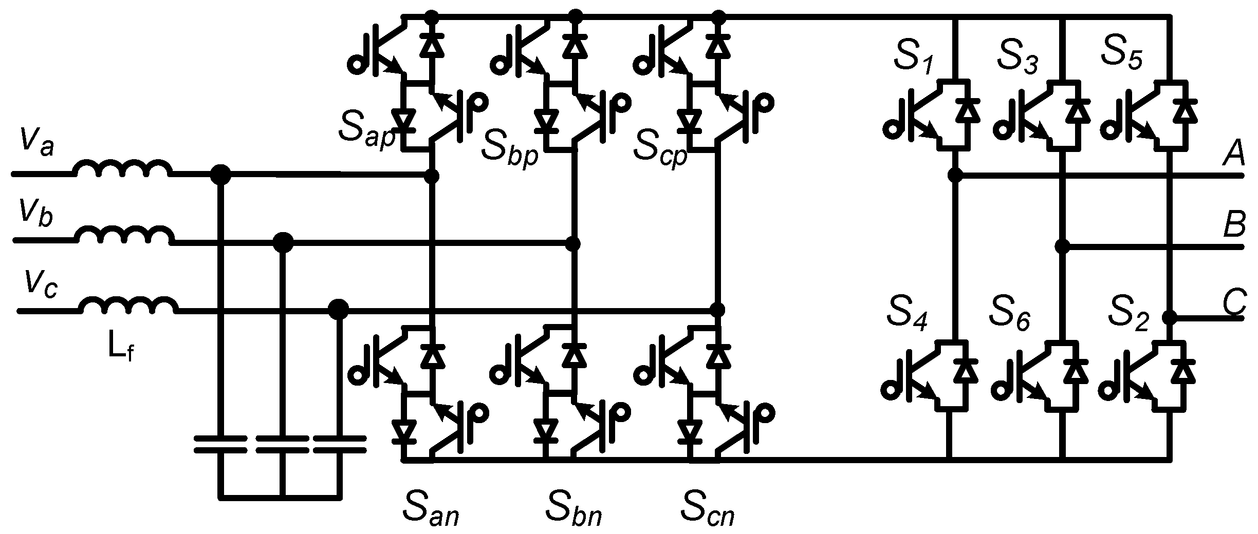
Over the past few years, there has been a significant effort towards addressing the technical challenges associated with the development of topology and control of the multilevel IMC. The conventional multilevel IMC topology was firstly introduced in [12], which is based on the traditional IMC, but with a rear-ends six-switch inverter replaced by a three-level neutral-point-clamped (NPC) inverter as shown in Figure 2. Then, the new multilevel IMC based on the combination of conventional NPC and cascaded-rectifier is presented in [13] in order to improve the voltage transfer ratio.
The common-mode voltage (CMV) is known as the main reason of the shaft voltage, leakage current, and bearing current damage, not only harms the motor lifetime, but also degrades the reliability of the electrical system. Thus, the techniques to reduce the CMV or to limit it within certain bounds are very important for the adjustable speed drive system which is fed by MC. The modulation strategies affect the CMV and several methods to reduce the CMV have been introduced in [3,14,15,16,17,18]. These SVPWM methods are suggested for conventional IMC and DMC to reduce the peak value of CMV by selecting the suitable zero switching states. The peak value of CMV in [14,18] is reduced to 42%. In [19,20], a new space vector modulation method to achieve zero CMV for DMC. However, the multi-step commutation and the limited of voltage transfer ratio are the advantages of the proposed method in [19,20]. Furthermore, in order to eliminate the CMV for DMC, only rotating vectors are used to synthesize the reference output voltage. Then, the output voltage performance is reduced.
Despite the multilevel IMC’s outstanding advantages, the common mode voltage (CMV) generated by PWM modulation is still problematic and it has received considerable attention to eliminate. In this paper, a novel approach of multilevel IMC topology is introduced. This topology is constructed based on the comprising of cascaded rectifier and the three-level T-Type NPC inverter. Furthermore, the SVPWM strategy is presented to eliminate the CMV with zero average value of neural-point current. The SVPWM modulation method with zero CMV (ZCMV) for the multilevel NPC inverter was first presented in [21]. This method uses the six active middle vectors and one zero vector due to their ability to create zero common mode voltage. However, the average value of the neutral-point current within one sampling period still exists, and it affects the neutral-point voltage. In this paper, the new SVPWM utilizes a group of four active vectors to produce the reference output voltage. These four active vectors consist of two active vectors closest to the reference vector and its two neighbor vectors. By apply four active vectors to synthesize the reference output voltage vector, the average value of neutral-point current is zero while the voltage transfer ratio was not affected. As compared to [3,14,15,16,17,18], the presented topology with proposed SVPWM method in this paper can provide the zero CMV.
The rest of this paper is organized as follows. Section 2 introduces the multilevel IMC topology and the SVPWM method to eliminate the CMV with canceling the neutral-point current. In Section 3, some simulation and experimental results are provided to illustrate the efficiency of the proposed method. Finally, conclusions are included in Section 4.
2. Multilevel Indirect Matrix Converter and the Proposed SVPWM Method
2.1. The Multilevel IMC Topology
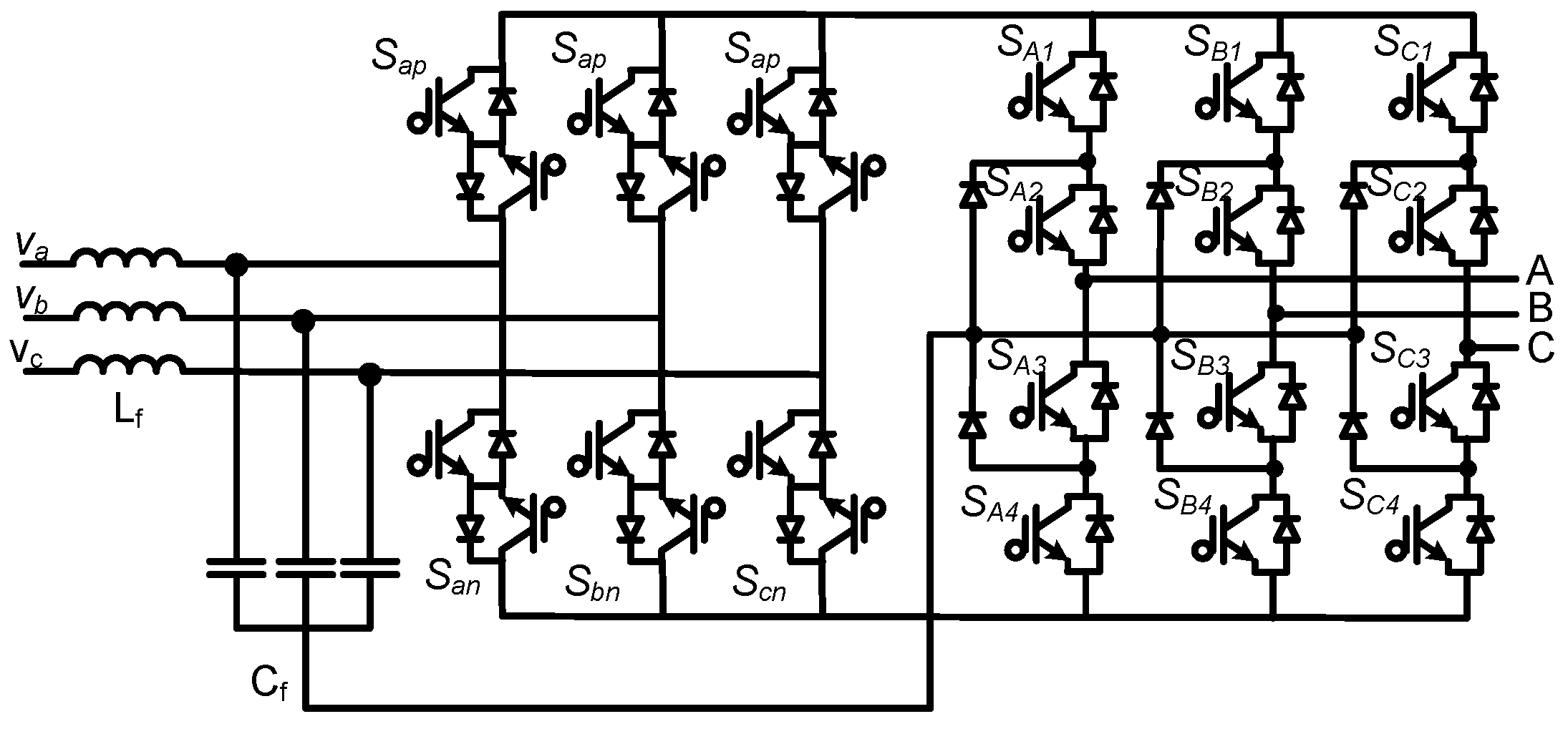
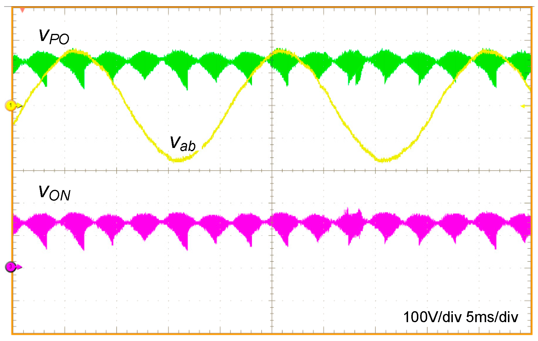
As shown in Figure 3, the multilevel IMC comprises of two stages: The rectifier stage and the three-level T-Type inverter stage. The function of the rectifier stage is to generate sinusoidal input currents as well as to maintain the maximum DC voltage at the DC-link. The expected output voltages with variable frequency are obtained by control at the inverter stage. The cascaded rectifier is built by two identical three-phase bidirectional front-end current source rectifier (CSR) modules connected in series [12]. Each CSR includes six bidirectional as shown in Figure 3 (Sap1, San1, Sbp1, Sbn1, Scp1, Scn1 for upper rectifier; and Sap2, San2, Sbp2, Sbn2, Scp2, Scn2 for lower rectifier), and they are connected at neutral-point “O”. The upper and lower rectifier stages generated the DC-link voltage: VPO and VON, respectively. The switching states at the rectifier stage and the DC-link voltage are shown in Table 1, where vab, vac, vbc, vba, vca, vcb are the line-to-line input voltage.
The three-level T-Type NPC inverter is the extension configuration of a traditional two-level three-phase inverter, by adding three bidirectional power switches that connect three-load output to the neutral point. Comparison with the traditional three-level NPC, the three-level T-Type NPC inverter have many advantages, e.g., less losses, less semiconductor components due to the absence of clamping diode [22,23]. From Figure 3, the switching state and load voltage of inverter stage are given in Table 2.
2.2. The SVPWM Method for Elimination the CMV
SVPWM techniques have been widely used for the power converter as a common industrial practice due to it has flexibility. The SVPWM is the general solution to the modulation problem of the IMC drive. This modulation can provide the possibility to obtain the highest voltage transfer ratio and to optimize the switching pattern by coordinate the switching state in the rectifier and inverter stages. The space vector approach for the multilevel IMC is based on the instantaneous space vector representation input current vector and output voltage vectors. The SVM produces a combination of vectors to synthesize the input current and output voltage vectors in the rectifier and inverter stages, respectively. Once the vectors and their duty cycles of each stage are determined, the switching pattern of the converter is obtained by combining the switching states from two stages in order to keep balance input and output currents. In this section, the novel SVPWM method is proposed to eliminate the CMV and to cancel the neutral-point current within the sampling period control.
2.2.1. Rectifier Stage Control
It is assumed that three-phase supply voltages va, vb, vc are given by:
where Vin is the amplitude of input phase voltage and ωin is the angular frequency of the input side.
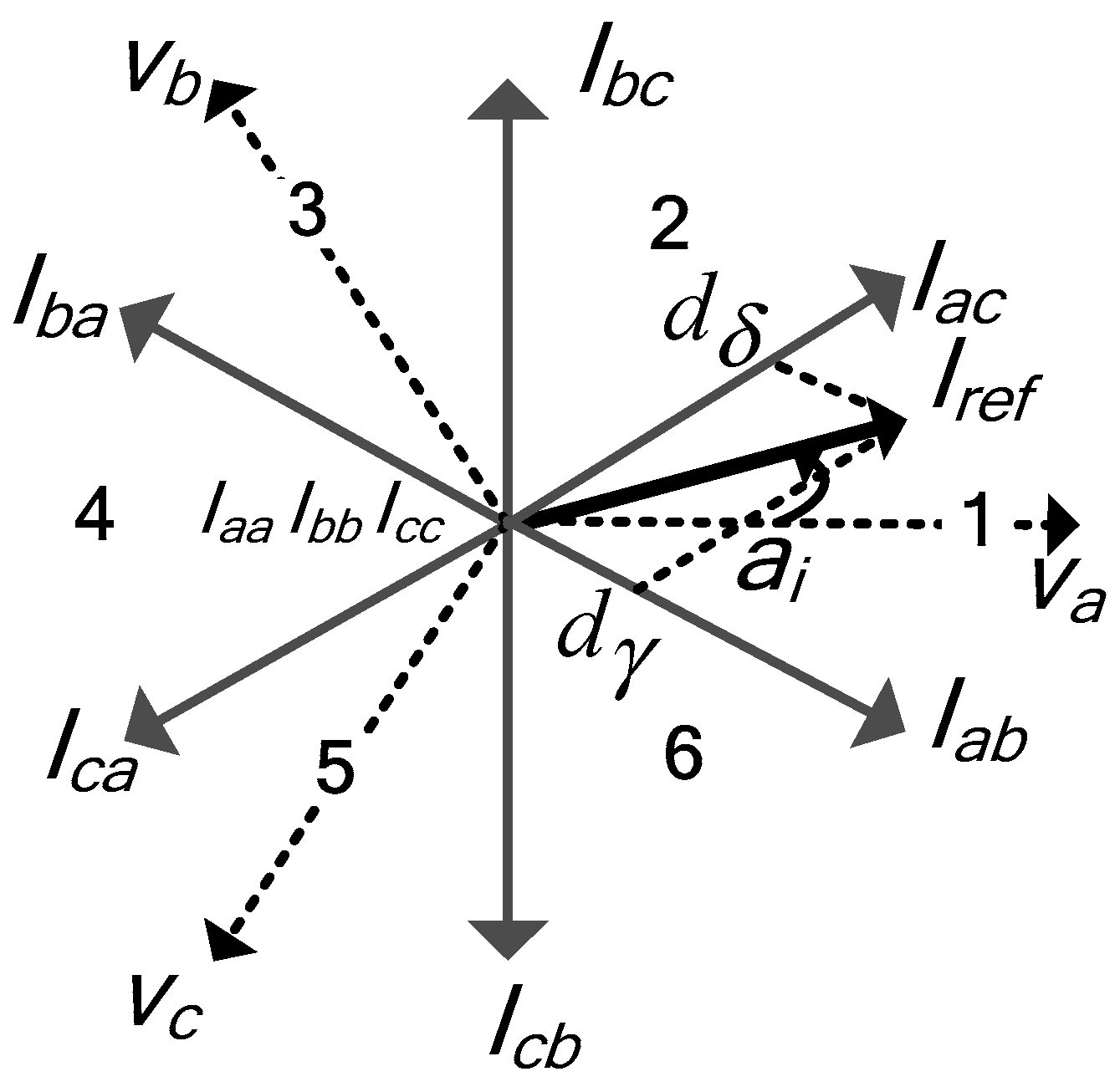
The current space vectors of the rectifier are illustrated in Figure 4. There are six active vectors with fixed direction and three zero vectors. Each active vector represents the connection of the input phase voltage to the positive, neutral or negative point of DC-link bus. In each sector, the reference current space vector is synthesized by two neighbor active vectors.
We assume that the reference current vector is located in sector 1 as shown in Figure 4. The duty cycles dγ, dδ of two active vectors Iab, Iac are given below:
where mi is the modulation index in the rectifier stage and αi is the phase angular of the reference input current.
Due to the elimination of zero vectors in the modulation of the rectifier stage to obtain the highest of DC-link voltage, the duty cycles of two active vectors is modified as following:
The local average value of DC-link voltage in one sampling period which is generated by the upper and lower rectifier can be written as:
Therefore, the average DC-link voltage is
Similarly, Table 3 summarizes the average of DC-link voltage, duty cycles of active vectors according to the input current sector.
2.2.2. Inverter Stage Control
Once the switching states of the rectifier stage have been decided, the SVPWM is applied to control the three-level T-Type NPC inverter. With the three-phase load, the system variables (voltages or currents) in abc coordinates can be transformed to αβ coordinates by using the transformation defined in (5).
where VA, VB, VC are three-phase output voltage and Vα, Vβ are corresponding voltage sequence in αβ plane given by Clark transform.
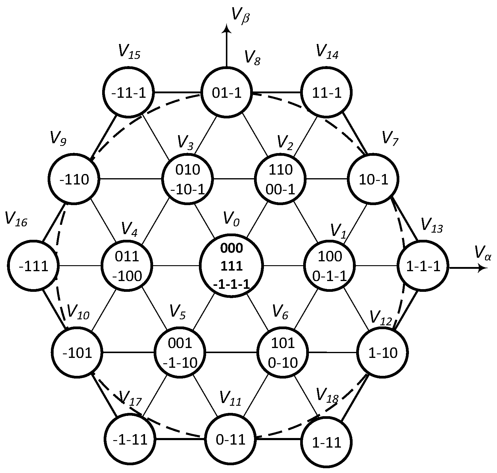
From (5), the size of each vector can be calculated and given in Table 4. The space vector diagram of the three-level T-type NPC inverter includes of 27 vectors which can be split into three categories: Zero, large, medium and small vectors. There are 6 large vectors, 6 medium vectors, 12 small vectors and 3 additional zero vectors as shown in Figure 5. On the plane vectors as shown in Figure 5, each vector indicates the connection of the output phase to the DC-link bus. For example, vector V13 (1-1-1) represents the connection of the output phase “A” to the positive pole “P”, output phase “B” and “C” to the negative pole “N” of DC-link bus.
There are three kinds of modulation strategies for three-level NPC inverter, i.e., carrier-based PWM, SVPWM and Selected Harmonics Elimination. Among three methods, the SVPWM has been a very popular PWM technique. In the space vector approach, over one PWM cycle, a specific number of voltage vectors are selected and used in a specific time length and sequence. The SVPWM with zero CMV was firstly presented in [21], but the neutral-point voltage imbalance stills exist due to the neutral-point current. In this paper, the novel SVPWM method is presented to obtain the zero CMV and to cancel the neutral-point current.
In the three-phase load, the CMV can be defined as a voltage between motor neutral point and ground point of power supply. The CMV can be described as follows:
where vCM is the common mode voltage; iA, iB, iC are three-phase output currents; R L are resistor and inductor of the load.
Under the assumption that the sum of output currents is equal to zero, iA + iB + iC = 0. The CMV can be obtained as follows:
From (7), Table 5 shows the CMV according to the state of the inverter stage.
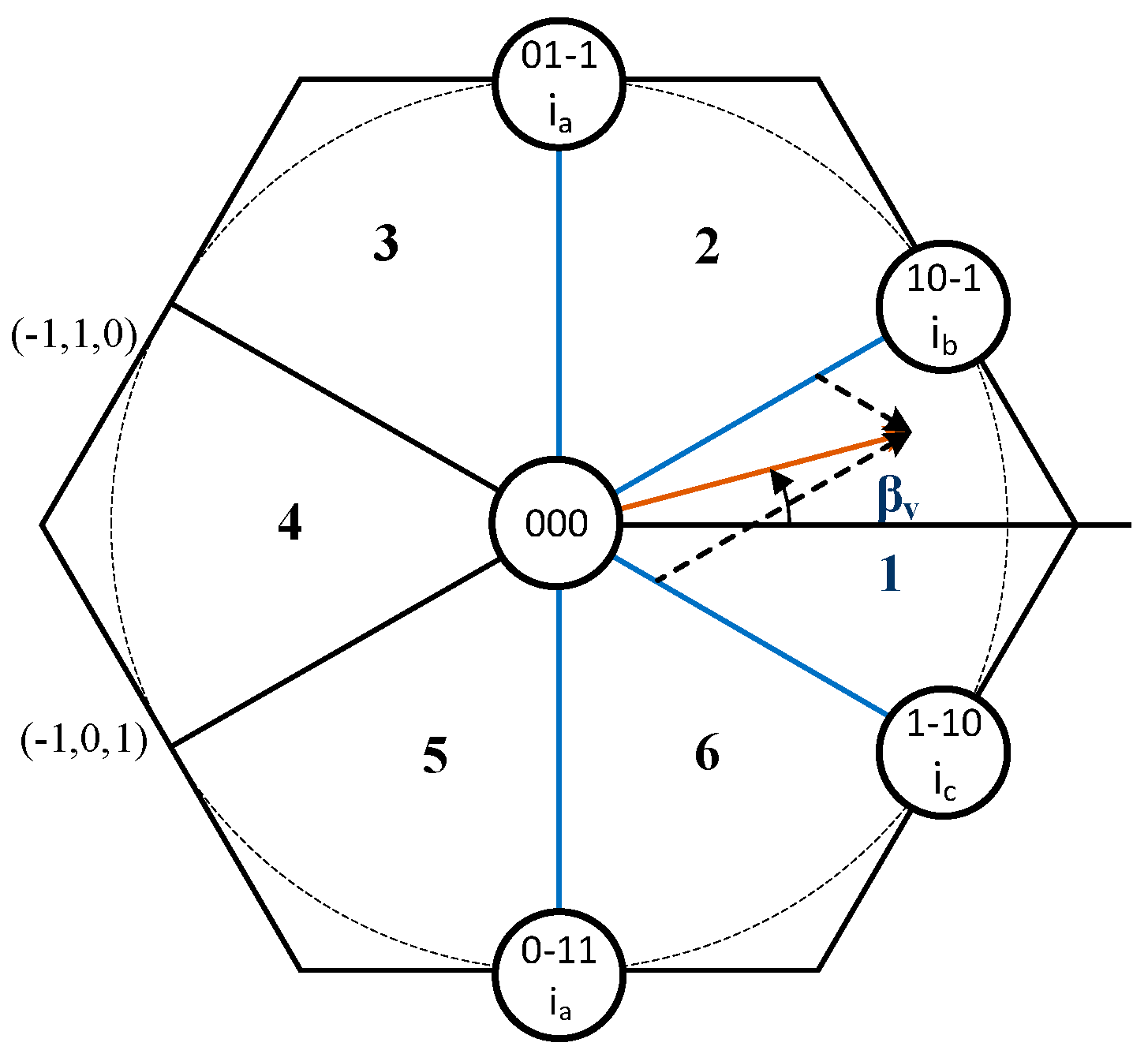
From Table 5, it can be easily seen that the magnitude of CMV has seven values: 0, ±VDC/6, ±VDC/3, ±VDC/2. In these 27 vectors, one zero and six medium vectors produce the ZCMV. The implementation of ZCMV modulation using an SVPWM approach is shown in Figure 6. It is assumed that the reference output voltage vector is in sector 1.
The reference voltage vector Vref can be obtained as:
where d01-1, d01-1, d1-10 and d0-11 are duty cycles of four active vectors V01-1, V10-1, V1-10 and V0-11, respectively.
When one phase leg is clamped to the neutral-point, its output current is injected to this point. Therefore, the average neutral-point current within sampling period is determined as:
The neutral-point current can be rewritten as:
where
To find the duty cycles of active vectors for obtaining the zero-average value of neutral-point current, the following two equations are used:
Substitute the (12), (13) to (8), we have:
From (10)–(14), the duty cycles of the active and zero vectors is calculated as following:
To complete one sampling period, the zero vector V000 is inserted and its duty cycle is calculated as:
where βv is a phase angle of reference output voltage vector (−π/6 ≤ βv ≤ π/6) and d000 are duty cycle of zero vector V000.
2.3. Maximum Voltage Transfer Ratio
If we define m as the voltage transfer ratio, which is the ratio between the output and input voltages, then:
From (4), the minimum values of the average DC-link voltage are:
All duty cycles must be positive and lower than unity, from (22) and (24), the maximum of reference output voltage is
From (8) and (20), the maximum voltage transfer ratio of the three-level T-Type NPC IMC is
2.4. Switching Sequence
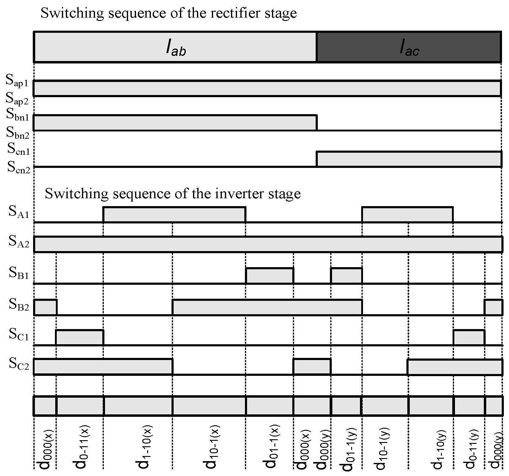
To obtain a balanced output currents and input currents, the PWM pattern of the multilevel IMC should produce all combinations between the switching states of the rectifier and the inverter stages. Figure 7 shows the switching sequence of the T-Type multilevel IMC in case of the reference input current and reference output voltage are located in sector 1 as shown in Figure 4; Figure 6, respectively. It is noted that the switching state of the rectifier and inverter stages are arranged to guarantee the zero DC-link current commutation at the rectifier stage, therefore the multi-step commutation is avoided.
The duty cycles for each voltage vector of the inverter stage can be determined using equations:
3. Simulation Results and Experimental Results
Simulations and experiments are carried out in order to verify the proposed method for multilevel IMC control. The simulation process is performed by using PSIM 9.1 software. The parameters of the system including power supply, load, sampling period control for simulation are given in Table 6.
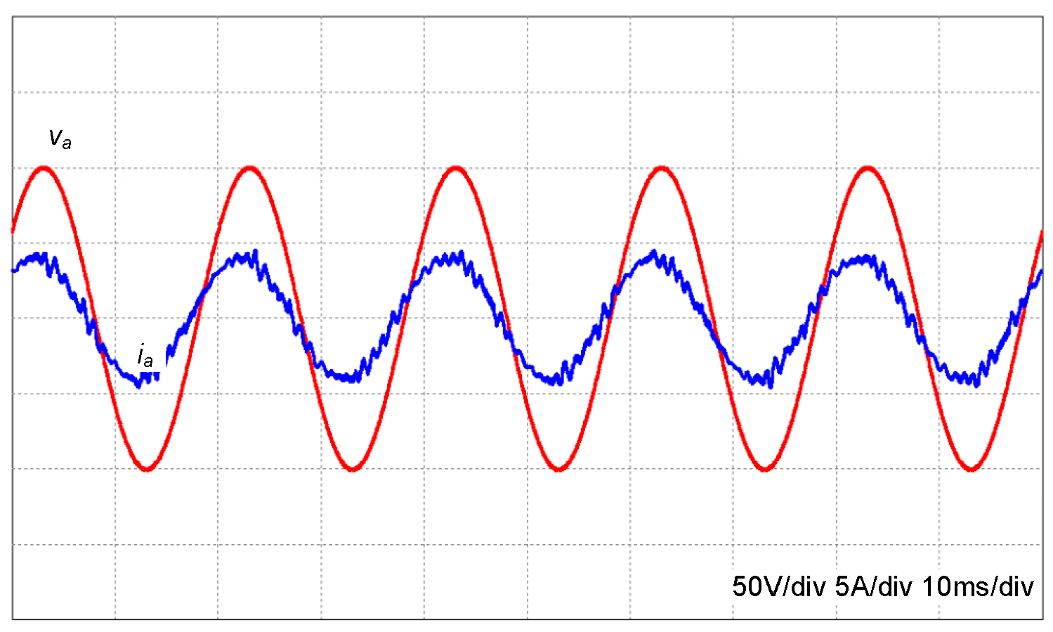
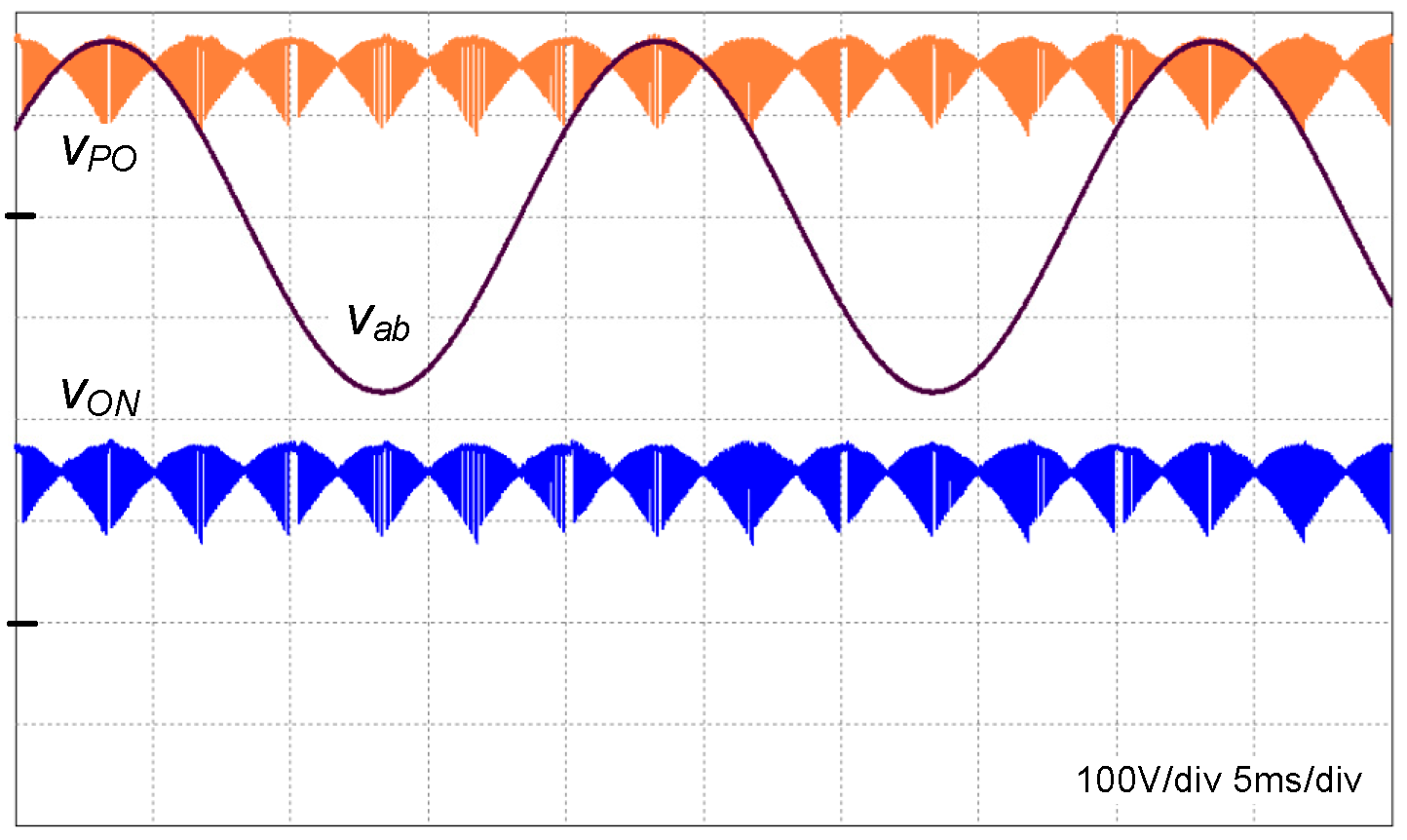
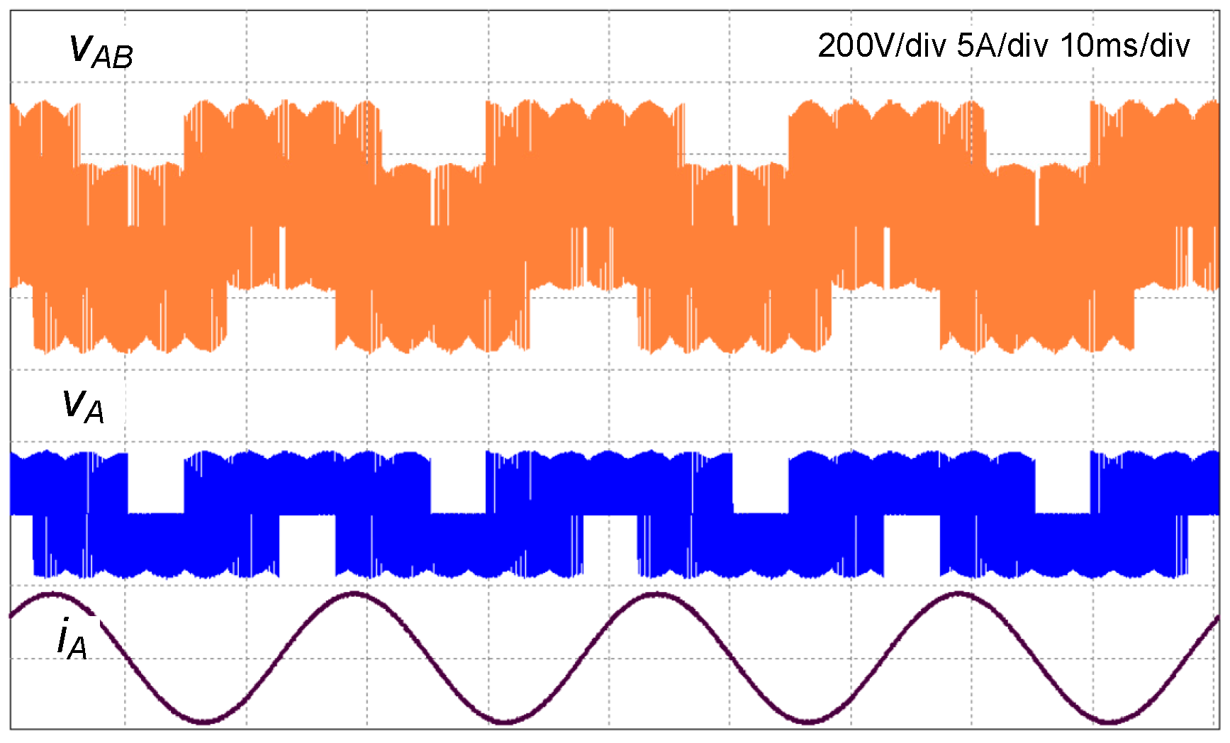
In Figure 8, the input phase voltage (va) and input phase current (ia) are shown. At the input side, the LC input filter is used to filter the switching frequency harmonic, therefore, the sinusoidal input current waveform is obtained. The input current and input voltage waveforms are almost in-phase. The dc-link voltage which is generated by the upper and lower rectifier stages is shown in Figure 9. It can be seen that the DC-link voltage does not consist of the zero voltage and it is modulated between the maximum and medium line-to-line input voltages. The shape of DC-link voltage is formed by the line-to-line input voltage and two dc-link voltages are the same value. The line-to-line output voltage (VAB), the phase output voltage (VA) and output current are shown in Figure 10; it is evident that output current is sinusoidal waveforms. In order to see the performance of the converter, the total harmonic distortion (THD) of the input current and the output voltage are shown in Table 7.
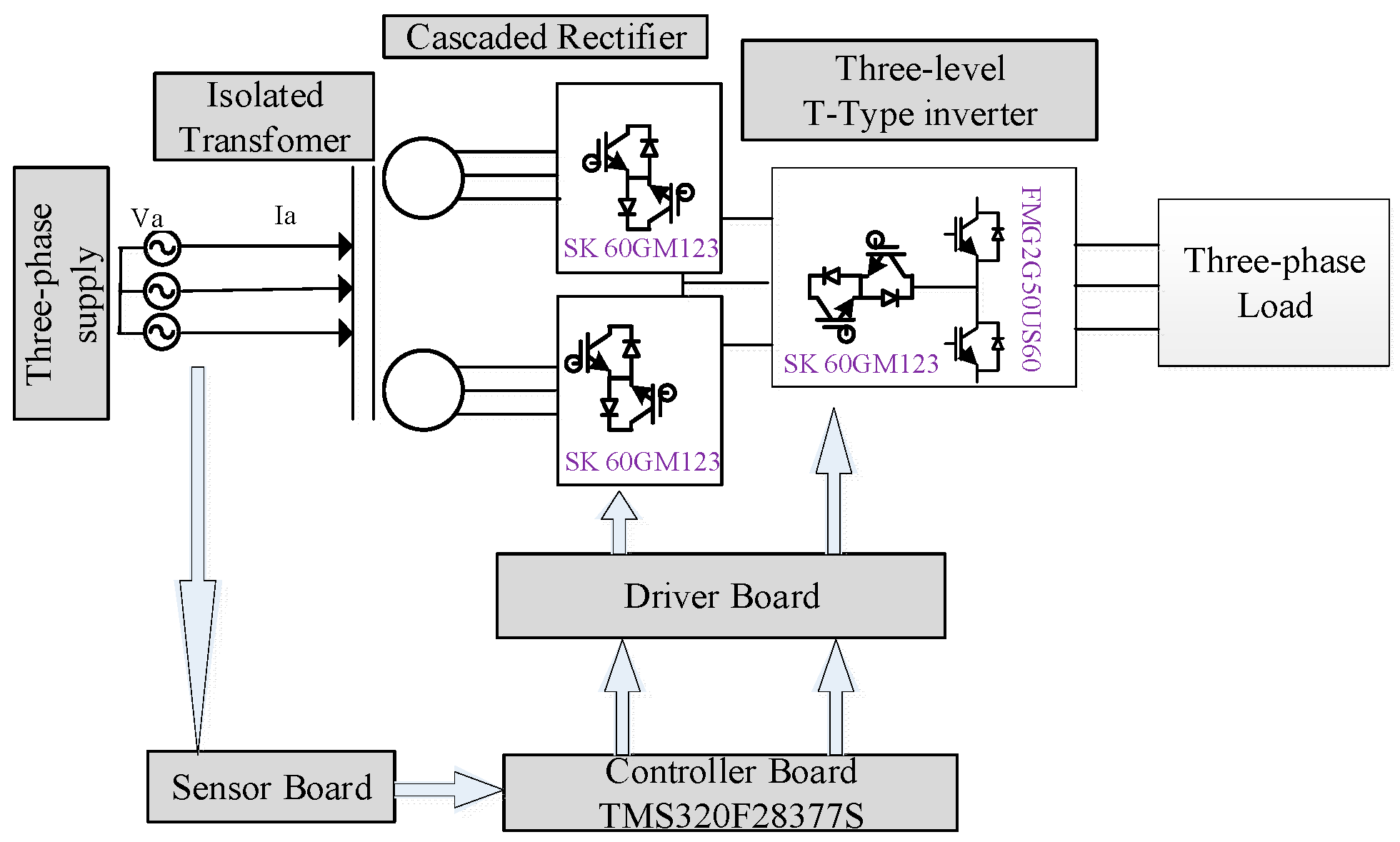
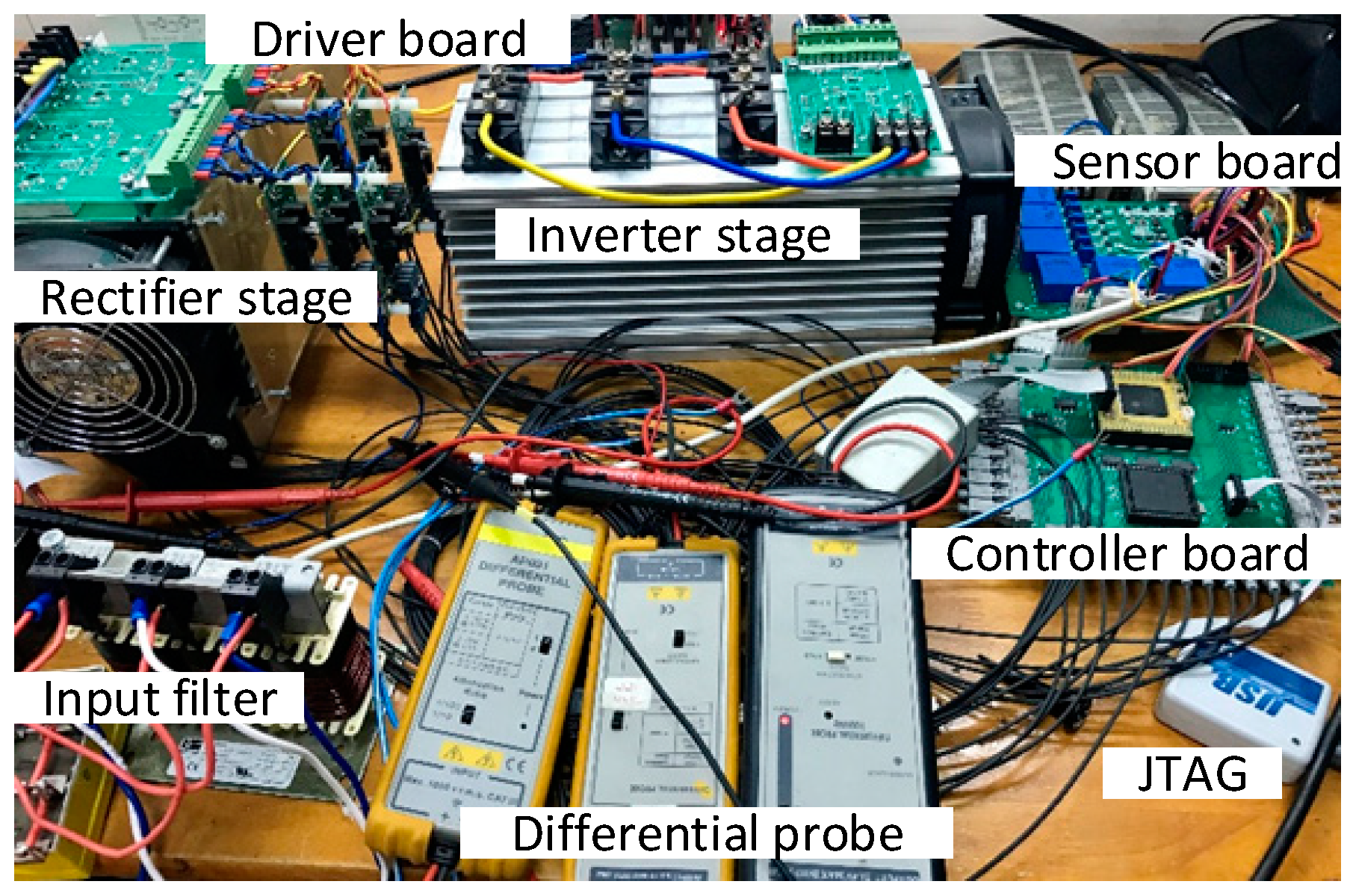
In order to confirm the propriety of the proposed topology, theory analysis and simulated results, an experiment for the proposed SVPWM method was built. The experimental parameters are identical to the simulation parameters. Figure 11 shows the block diagram of a multilevel IMC and Figure 12 indicates the photograph of the experimental setup. The system consists of a controller board, power board, sensor board and driver board. The controller board is developed with a high-performance DSP TMS320F28377S, which executes the A/D converter, the generating PWM signals for driver circuit. The sensor board uses the LV-25P of LEM. The power board was implemented by using IGBT SK 60GM123 for bidirectional switches and IGBT FMG2G50U60 for dual switch in the inverter stage. Table 8 lists the model name, manufacturer and the ratings of the power switches used in the power converter.
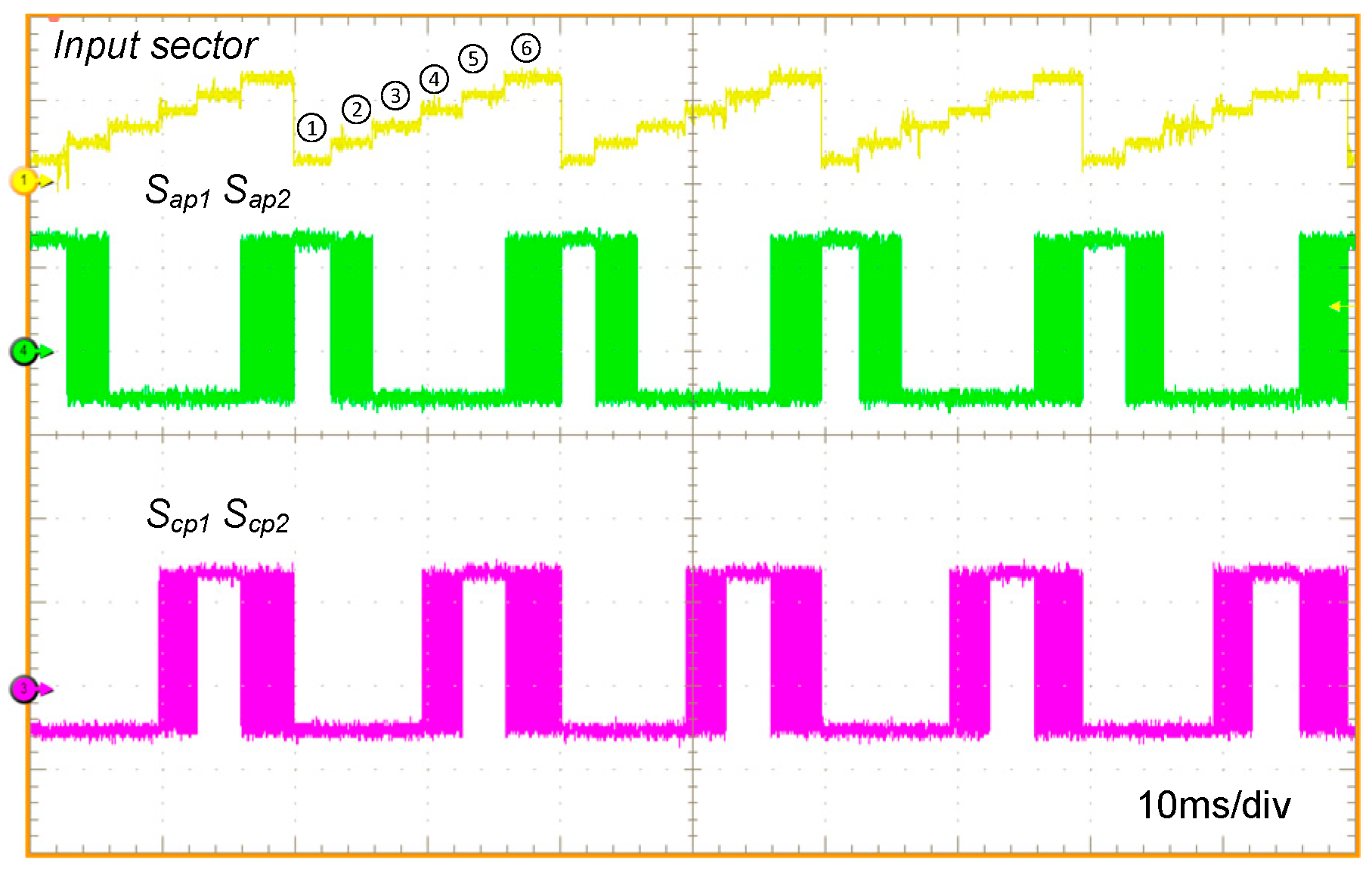
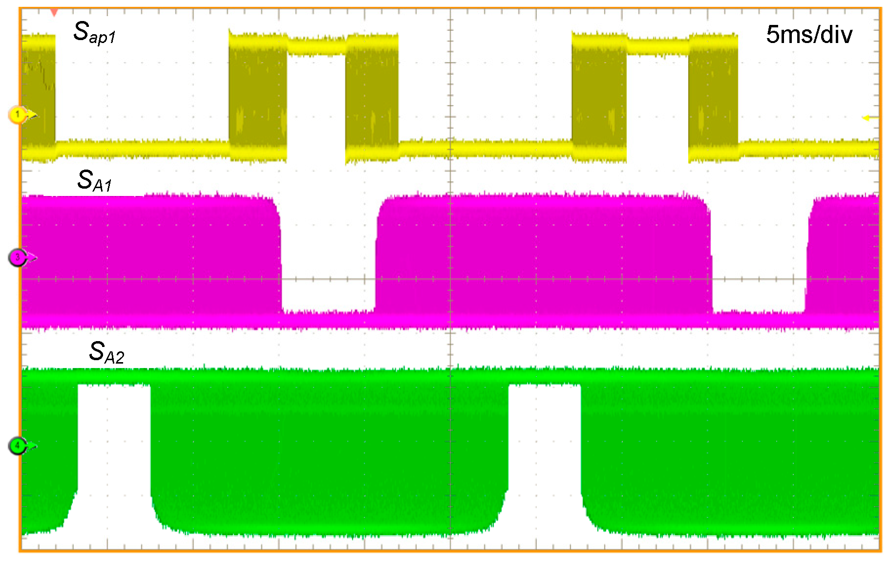
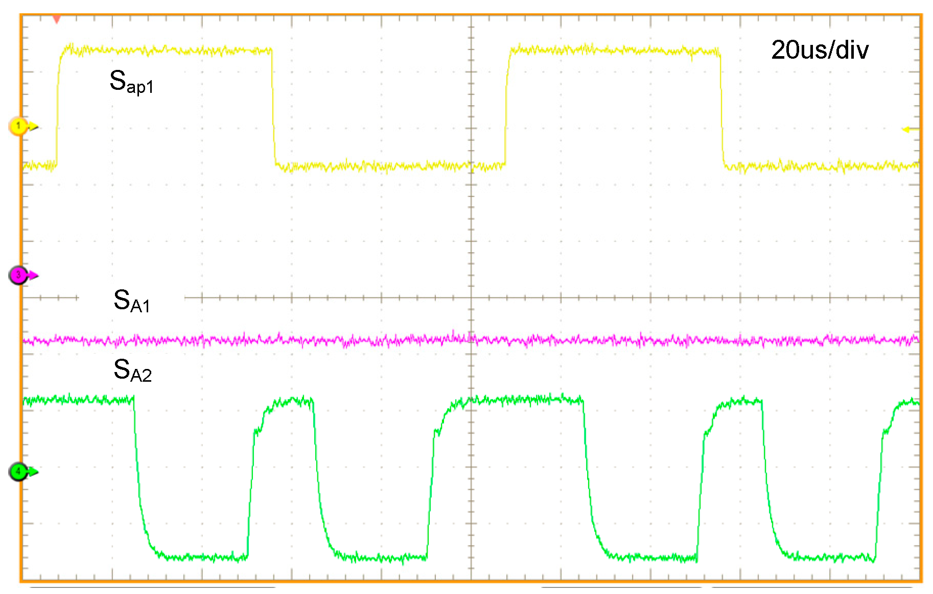
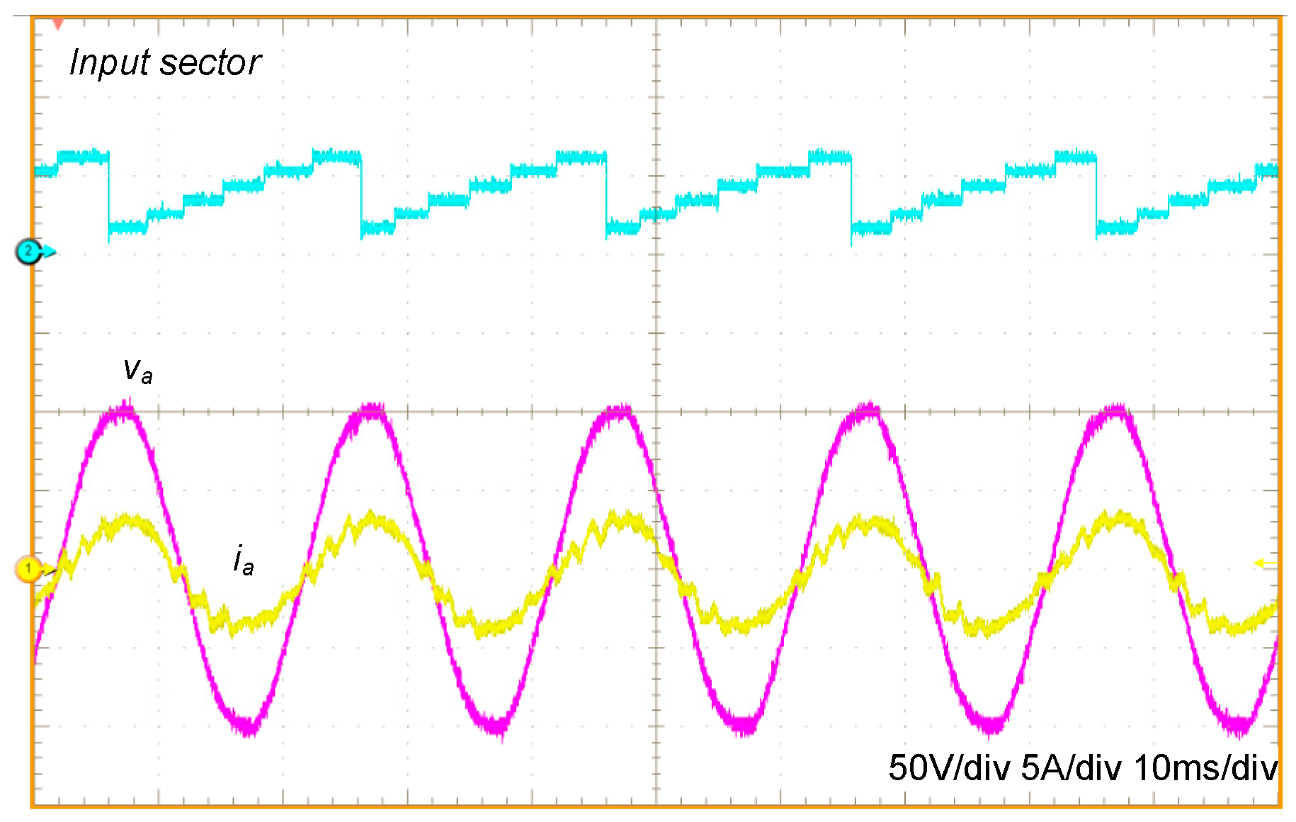
The pulse signals for the rectifier stage according to the input sector are shown in Figure 13. It can be seen that, the switch Sap1, Sap2 are always at ON state in sector 1, they are modulated in sector 2 and 6 and at OFF state in all remain sectors. Figure 14 shows the PWM signals for the rectifier and inverter stages, and the zoom in of these waveforms is shown in Figure 15. From Figure 15, the switch Sap1 of the rectifier stage changes the status from ON to OFF or OFF to ON during the time when the zero vector is applied in the inverter stage (SA1 is OFF state and SA2 is ON state). It means that the soft-switching is achieved in the rectifier stage.
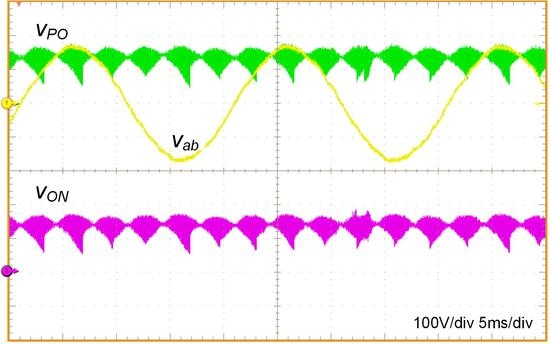
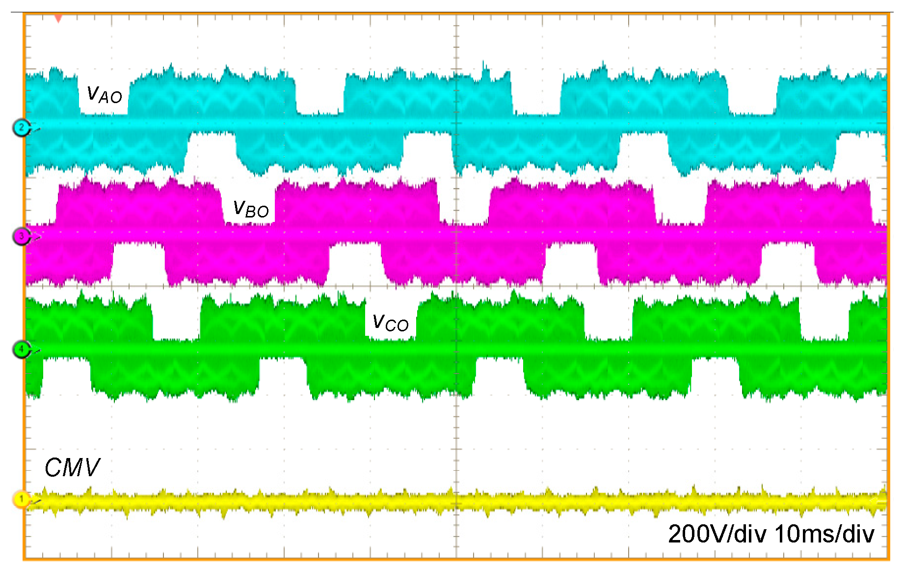
The experimental results of input side, DC-link voltage and output side are shown in Figure 16, Figure 17 and Figure 18, respectively. It can be seen that both of the input current and output current are sinusoidal waveforms. However, the input current contains some ripple due to the limitation of input LC filter. Furthermore, the level of output voltages of the multilevel IMC is higher than that of conventional two-level IMC. Figure 19 shows the phase-to-neutral point voltage and the common mode voltage. The zero common mode voltage is obtained with the proposed method.
4. Conclusions
We have introduced the novel approach of multilevel IMC and proposed SVPWM method with zero common mode voltage. The explanation of multilevel IMC operating and duty cycles calculating are provided. Both simulation and experimental results are shown to demonstrate the effectiveness of the proposed method. Besides the advantageous features of the conventional MC, i.e., compact design, sinusoidal input/output current, bidirectional power flow, we have figured out other features to compensate for the drawbacks of the IMC, i.e., used two cascaded-rectifier to improve the voltage transfer ratio, proposed new SVPWM method to obtain zero CMV with neutral-point voltage balancing.
Author Contributions
N.D.T. developed the idea of this paper, implemented the main research and validated in the real system. L.M.P. performed the analysis and simulation. All authors contributed to the writing of the manuscript, revised and approved the final manuscript.
Funding
This research is funded by Vietnam National Foundation for Science and Technology Development (NAFOSTED) under grant number 103.99-2015.102.
Conflicts of Interest
The authors declare no conflict of interest.
References
- Wheeler, P.; Rodriguez, J.; Clare, J.; Empringham, L.; Weinstein, A. Matrix converters: A technology review. IEEE Trans. Ind. Electron. 2002, 49, 276–288. [Google Scholar] [CrossRef]
- Kolar, J.W.; Friedli, T.; Rodriguez, J.; Wheeler, P.W. Review of Three-Phase PWM AC–AC Converter Topologies. IEEE Trans. Ind. Electron. 2011, 58, 4988–5006. [Google Scholar] [CrossRef]
- Nguyen, T.D.; Lee, H.-H. Modulation Strategies to Reduce Common-Mode Voltage for Indirect Matrix Converters. IEEE Trans. Ind. Electron. 2012, 59, 129–140. [Google Scholar] [CrossRef]
- Guo, Y.; Wang, X.; Guo, Y.; Deng, W. Speed-sensorless direct torque control scheme for matrix converter driven induction motor. J. Eng. 2018, 2018, 432–437. [Google Scholar] [CrossRef]
- Riedemann, J.; Andrade, I.; Peña, R.; Blasco-Gimenez, R.; Clare, J.; Melín, P.; Rivera, M. Modulation strategies for an open-end winding induction machine fed by a two-output indirect matrix converter. Math. Comput. Simul. 2016, 130, 95–111. [Google Scholar] [CrossRef] [Green Version]
- Arevalo, S.L.; Zanchetta, P.; Wheeler, P.W.; Trentin, A.; Empringham, L. Control and Implementation of a Matrix-Converter-Based AC Ground Power-Supply Unit for Aircraft Servicing. IEEE Trans. Ind. Electron. 2010, 57, 2076–2084. [Google Scholar] [CrossRef]
- Barakati, M.; Kazerani, M.; Aplevich, J. Maximum Power Tracking Control for a Wind Turbine System Including a Matrix Converter. IEEE Trans. Convers. 2009, 24, 705–713. [Google Scholar] [CrossRef]
- Wei, L.; Lipo, T.A. A novel matrix converter topology with simple commutation. In Proceedings of the Thirty-Sixth IAS Annual Meeting, Conference Record of the 2001 IEEE Industry Applications Conference, Chicago, IL, USA, 30 September–4 October 2001; Volume 3, pp. 1749–1754. [Google Scholar]
- Shi, Y.; Yang, X.; He, Q.; Wang, Z. Research on a Novel Capacitor Clamped Multilevel Matrix Converter. IEEE Trans. Electron. 2005, 20, 1055–1065. [Google Scholar] [CrossRef]
- Rmili, L.; Hamouda, M.; Rahmani, S.; Al-Haddad, K. Advanced topologies of multilevel matrix converter. In Proceedings of the 2015 16th International Conference on Sciences and Techniques of Automatic Control and Computer Engineering (STA), Monastir, Tunisia, 21–23 December 2015; pp. 599–604. [Google Scholar]
- Lee, M.Y.; Wheeler, P.; Klumpner, C. Space-Vector Modulated Multilevel Matrix Converter. IEEE Trans. Ind. Electron. 2010, 57, 3385–3394. [Google Scholar] [CrossRef]
- Loh, P.C.; Blaabjerg, F.; Gao, F.; Baby, A.; Tan, D.A.C. Pulsewidth Modulation of Neutral-Point-Clamped Indirect Matrix Converter. IEEE Trans. Ind. Appl. 2008, 44, 1805–1814. [Google Scholar] [CrossRef]
- Sun, Y.; Xiong, W.; Su, M.; Li, X.; Dan, H.; Yang, J. Topology and Modulation for a New Multilevel Diode-Clamped Matrix Converter. IEEE Trans. Electron. 2014, 29, 6352–6360. [Google Scholar] [CrossRef]
- Nguyen, T.D.; Lee, H.-H. A New SVM Method for an Indirect Matrix Converter With Common-Mode Voltage Reduction. IEEE Trans. Ind. Informat. 2014, 10, 61–72. [Google Scholar] [CrossRef]
- Padhee, V.; Sahoo, A.; Ned, M. Modulation Techniques for Enhanced Reduction in Common Mode Voltage and Output Voltage Distortion in Indirect Matrix Converters. IEEE Trans. Electron. 2017, 32, 1. [Google Scholar] [CrossRef]
- Rahman, K.; Al-Emadi, N.; Iqbal, A.; Rahman, S. Common mode voltage reduction technique in a three-to-three phase indirect matrix converter. IET Electr. Appl. 2018, 12, 254–263. [Google Scholar] [CrossRef]
- Cha, H.J.; Enjeti, P.N. An approach to reduce common mode voltage in matrix converter. IAS-02 2003, 1, 432–437. [Google Scholar]
- Guan, Q.; Wheeler, P.; Yang, P. Common-mode Voltage Reduction for Matrix Converters Using All Valid Switch States. IEEE Trans. Electron. 2016, 31, 1. [Google Scholar] [CrossRef]
- Nguyen, H.; Lee, H. A Modulation Scheme for Matrix Converters With Perfect Zero Common-Mode Voltage. IEEE Trans. Power Electron. 2016, 31, 5411–5422. [Google Scholar] [CrossRef]
- Nguyen, H.-N.; Lee, H.-H.; Huu-Nhan, N. A DSVM Method for Matrix Converters To Suppress Common-mode Voltage with Reduced Switching Losses. IEEE Trans. Electron. 2016, 31, 1. [Google Scholar] [CrossRef]
- Wang, F.; Wallace, A.; Dai, S.; Von Jouanne, A.; Zhang, H. Multilevel inverter modulation schemes to eliminate common-mode voltages. IEEE Trans. Ind. Appl. 2000, 36, 1645–1653. [Google Scholar] [CrossRef]
- Cailhol, S.; Vidal, P.; Rotella, F. A Generic Method of Pulse width Modulation Applied to Three-Phase Three-Level T-Type NPC Inverter. IEEE Trans. Ind. Appl. 2018, 54, 4515–4522. [Google Scholar] [CrossRef]
- Wang, Y.; Shi, W.W.; Xie, N.; Wang, C.M. Diode-Free T-Type Three-Level Neutral-Point-Clamped Inverter for Low-Voltage Renewable Energy System. IEEE Trans. Ind. Electron. 2014, 61, 6168–6174. [Google Scholar] [CrossRef]
Figure 1.
The conventional Indirect Matrix Converter topology.

Figure 2.
The conventional NPC multilevel Indirect Matrix Converter.

Figure 3.
The Three-level T-Type Indirect Matrix Converter Topology.

Figure 4.
The space vector diagram of the rectifier stage.

Figure 5.
The space vector diagram of the 3-level T-Type NPC inverter stage.

Figure 6.
Space vector diagram and the selected vectors for zero common voltage.

Figure 7.
The switching pattern of the multilevel IMC with the proposed SVPWM method.

Figure 8.
The simulation results of input current and input voltage.

Figure 9.
The simulation results of DC-link voltage VPO and VON, which are generated by the upper and lower rectifiers, respectively.
Figure 9.
The simulation results of DC-link voltage VPO and VON, which are generated by the upper and lower rectifiers, respectively.

Figure 10.
The simulation results of line-to-line output voltage, phase output voltage and output current.
Figure 10.
The simulation results of line-to-line output voltage, phase output voltage and output current.

Figure 11.
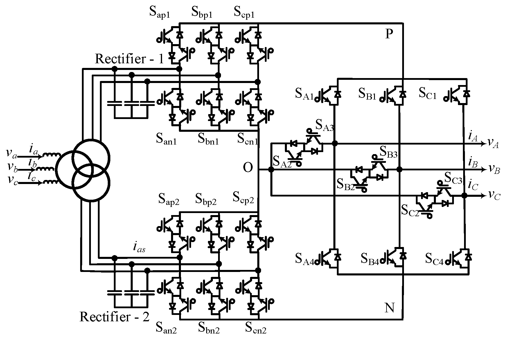
Block diagram of the multilevel IMC hardware experiment.

Figure 12.
Experimental setup.

Figure 13.
Input sector and the PWM signals of rectifier stages.

Figure 14.
The PWM signals of rectifier and inverter stages.

Figure 15.
The zoom-in of PWM signals of rectifier and inverter stages.

Figure 16.
Experimental results of input side.

Figure 17.
Experimental results of DC-link voltage.

Figure 18.
Experimental results of load side: line-to-line output voltage, phase output voltage and output current.
Figure 18.
Experimental results of load side: line-to-line output voltage, phase output voltage and output current.

Figure 19.
The phase to neutral voltage and the common mode voltage.


Table 1.
The switching states at rectifier stage and the DC-link voltage.
| Switching State | DC-Link Voltage | ||||||
|---|---|---|---|---|---|---|---|
| Sap1 | Sbp1 | Scp1 | San1 | Sbn1 | Scn1 | VPO | VON |
| Sap2 | Sbp2 | Scp2 | San2 | Sbn2 | Scn2 | ||
| 1 | 0 | 0 | 0 | 1 | 0 | vab | vab |
| 1 | 0 | 0 | 0 | 0 | 1 | vac | vac |
| 0 | 1 | 0 | 0 | 0 | 1 | vbc | vbc |
| 0 | 1 | 0 | 1 | 0 | 0 | vba | vba |
| 0 | 0 | 1 | 1 | 0 | 0 | vca | vca |
| 0 | 0 | 1 | 0 | 1 | 0 | vcb | vcb |
| 1 | 0 | 0 | 1 | 0 | 0 | 0 | 0 |
| 0 | 1 | 0 | 0 | 1 | 0 | 0 | 0 |
| 0 | 0 | 1 | 0 | 0 | 1 | 0 | 0 |
Table 2.
The state of inverter stage and the output voltage according to the switching state.
| Inverter Stage’s State | Switching State of Power Switches X = (A, B, C) | Output-Phase Voltage VXO X = (A, B, C) | |||
|---|---|---|---|---|---|
| SX1 | SX2 | SX3 | SX4 | ||
| 1 | 1 | 1 | 0 | 0 | VPO |
| 0 | 0 | 1 | 1 | 0 | 0 |
| −1 | 0 | 0 | 1 | 1 | −VON |
Table 3.
Switching state and average DC link voltage according to the input current sector.
| Input Voltage Phase ωint | Sector | ON Switch | Modulated Switches | Duty Ratios | Instantaneous Split DC-Link Voltages | Average DC-Link Voltage vPN |
|---|---|---|---|---|---|---|
| Upper Rectifier | (dx, dy) | VPO | ||||
| Lower Rectifier | (dx, dy) | VON | ||||
| −π/6 π/6 | I | Sap1 | (Sbn1, Scn1) | (−vb/va, −vc/va) | vab vac | |
| Sap2 | (Sbn2, Scn2) | |||||
| π/6 π/2 | II | Scn1 | (Sbp1, Sap1) | (−vb/vc, −va/vc) | vbc vac | |
| Scn2 | (Sbp2, Sap2) | |||||
| π/2.5π/6 | III | Sbp1 | (Scn1, San1) | (−vc/vb, −va/vb) | vbc vba | |
| Sbp2 | (Scn2, San2) | |||||
| 5π/6.7π/6 | IV | San1 | (Scp1, Sbp1) | (−vc/va, −vb/va) | vca vba | |
| San2 | (Scp2, Sbp2) | |||||
| 7π/6.9π/6 | V | Scp1 | (San1, Sbn1) | (−vb/vc, −vb/va) | vcb vca | |
| Scp2 | (San2, Sbn2) | |||||
| 9π/6.11π/6 | VI | Sbn1 | (Scp1, Sap1) | (−vc/vb, −va/vb) | vab vcb | |
| Sbn2 | (Scp2, Sap2) | (-vc/vb, −va/vb) | ||||
Table 4.
Space vectors, switching states and type of vectors.
| Space Vectors | Switching States | Type of Vector | Vector Magnitude | ||
|---|---|---|---|---|---|
| (−1,−1,−1) | 0 | 0 | Zero vector | 0 | |
| (0,0,0) | 0 | 0 | |||
| (1,1,1) | 0 | 0 | |||
| (1,0,0) | 0 | Small vector | |||
| (0,−1,−1) | 0 | ||||
| (1,1,0) | |||||
| (0,0,−1) | |||||
| (0,1,0) | |||||
| (−1,0,−1) | |||||
| (0,1,1) | 0 | ||||
| (−1,0,0) | 0 | ||||
| (0,0,1) | |||||
| (−1,−1,0) | |||||
| (1,0,1) | |||||
| (0,−1,0) | |||||
| (1,0,−1) | Medium Vector | ||||
| (0,1,−1) | 0 | ||||
| (−1,1,0) | |||||
| (−1,0,1) | |||||
| (0,−1,1) | 0 | ||||
| (1,−1,0) | |||||
| (1,−1,−1) | 0 | Large vector | |||
| (1,1,−1) | |||||
| (−1,1,−1) | |||||
| (−1,1,1) | 0 | ||||
| (−1,−1,1) | |||||
| (1,−1,1) |
Table 5.
The CMV of the 3-level T-Type NPC inverter.
| Inverter Stage’s Switching State | Common Mode Voltage |
|---|---|
| (0,0,0) | 0 |
| (−1,−1,−1) | −VDC/2 |
| (1,1,1) | VDC/2 |
| (1,0,0); (0,1,0); (0,0,1); (−1,1,1); (1,−1,1); (1,1,−1) | VDC/6 |
| (0,0,−1); (−1,0,0); (0,−1,0); (1,−1,−1); (−1,1,−1); (−1,−1,1) | −VDC/6 |
| (1,0,−1); (0,1,−1); (−1,1,0); (−1,0,1); (0,−1,1); (1,−1,0) | 0 |
| (1,1,0); (1,0,1); (0,1,1) | VDC/3 |
| (0,−1,−1); (−1,0,−1); (−1,−1,0) | −VDC/3 |
Table 6.
The parameter for simulation and experimental.
| Input voltage (Vin) | 100 V |
| Input frequency (fin) | 50 Hz |
| R load | 20 Ω |
| L load | 20 mH |
| Output frequency (fout) | 40 Hz |
| Sampling period (Ts) | 100 kHz |
| Voltage transfer ratio (m) | 1.2 |
Table 7.
The THD of input current and output voltage according to the voltage transfer ratio.
| Voltage Transfer Ratio (m) | THD of Input Current (%) | THD of Output Voltage |
|---|---|---|
| 0.2 | 0.42 | 6.48 |
| 0.4 | 1.52 | 4.57 |
| 0.6 | 2.62 | 3.48 |
| 0.8 | 3.80 | 2.76 |
| 1.0 | 4.55 | 2.30 |
| 1.2 | 6.20 | 1.94 |
| 1.4 | 6.82 | 1.60 |
Table 8.
Summary of IGBT Module for the converter.
| Model Name | Manufacturer | Rated Voltage | Rated Current | Power Switches in Figure 3 |
|---|---|---|---|---|
| SK 60GM123 | Semikron | 1200 V | 50 A | Sap1, San1, Sbp1, Sbn1, Scp1,Scn1 Sap2, San2, Sbp2, Sbn2, Scp2,Scn2 SA2, SA3, SB2, SB3, SC2, SC3 |
| FMG 2G 50US60 | Fairchild Semiconductor | 600 V | 50 A | SA1, SA4, SB1, SB4, SC1, SC4 |
© 2019 by the authors. Licensee MDPI, Basel, Switzerland. This article is an open access article distributed under the terms and conditions of the Creative Commons Attribution (CC BY) license (http://creativecommons.org/licenses/by/4.0/).
Share and Cite
MDPI and ACS Style
Dinh Tuyen, N.; Minh Phuong, L. SVPWM Method for Multilevel Indirect Matrix Converter with Eliminate Common Mode Voltage. Appl. Sci. 2019, 9, 1342. https://0-doi-org.brum.beds.ac.uk/10.3390/app9071342
AMA Style
Dinh Tuyen N, Minh Phuong L. SVPWM Method for Multilevel Indirect Matrix Converter with Eliminate Common Mode Voltage. Applied Sciences. 2019; 9(7):1342. https://0-doi-org.brum.beds.ac.uk/10.3390/app9071342
Chicago/Turabian StyleDinh Tuyen, Nguyen, and Le Minh Phuong. 2019. "SVPWM Method for Multilevel Indirect Matrix Converter with Eliminate Common Mode Voltage" Applied Sciences 9, no. 7: 1342. https://0-doi-org.brum.beds.ac.uk/10.3390/app9071342
Note that from the first issue of 2016, this journal uses article numbers instead of page numbers. See further details here.