Exceedingly High Performance Top-Gate P-Type SnO Thin Film Transistor with a Nanometer Scale Channel Layer


1
Department of Electronics Engineering, National Chiao Tung University, Hsinchu 300, Taiwan
2
Rzhanov Institute of Semiconductor Physics, Siberian Branch, Russian Academy of Sciences, Novosibirsk 630090, Russia
3
Novosibirsk State University, 2 Pirogov Street, Novosobirsk 630090, Russia
4
Novosibirsk State Technical University, 20 Marks Avenue, Novosibirsk 630073, Russia
*
Author to whom correspondence should be addressed.
Nanomaterials 2021, 11(1), 92; https://0-doi-org.brum.beds.ac.uk/10.3390/nano11010092
Submission received: 16 December 2020
/
Revised: 30 December 2020
/
Accepted: 30 December 2020
/
Published: 3 January 2021
(This article belongs to the Special Issue Nanoscience and Nanotechnology for Electronics)
Abstract
:Implementing high-performance n- and p-type thin-film transistors (TFTs) for monolithic three-dimensional (3D) integrated circuit (IC) and low-DC-power display is crucial. To achieve these goals, a top-gate transistor is preferred to a conventional bottom-gate structure. However, achieving high-performance top-gate p-TFT with good hole field-effect mobility (μFE) and large on-current/off-current (ION/IOFF) is challenging. In this report, coplanar top-gate nanosheet SnO p-TFT with high μFE of 4.4 cm2/Vs, large ION/IOFF of 1.2 × 10⁵, and sharp transistor’s turn-on subthreshold slopes (SS) of 526 mV/decade were achieved simultaneously. Secondary ion mass spectrometry analysis revealed that the excellent device integrity was strongly related to process temperature, because the HfO2/SnO interface and related μFE were degraded by Sn and Hf inter-diffusion at an elevated temperature due to weak Sn–O bond enthalpy. Oxygen content during process is also crucial because the hole-conductive p-type SnO channel is oxidized into oxygen-rich n-type SnO2 to demote the device performance. The hole μFE, ION/IOFF, and SS values obtained in this study are the best-reported data to date for top-gate p-TFT device, thus facilitating the development of monolithic 3D ICs on the backend dielectric of IC chips.
1. Introduction
Metal-oxide Thin film transistors (TFTs) [1,2,3,4,5,6,7,8,9,10,11,12,13,14,15,16,17,18,19,20,21,22,23,24,25,26,27,28,29,30,31,32,33,34,35] have drawn considerable attention due to their high mobility, low fabrication temperature, and simple fabrication process, making them suitable for advanced display [1,2,3,4,5,6] and monolithic three-dimensional (3D) integrated circuit (IC) [15,16,17,18,19,20,21] on amorphous inter-metal-dielectric (IMD) of a Si chip. To reach low DC power consumption, both high performance n- and p-type TFTs are necessary to form the complementary metal-oxide-semiconductor (CMOS) logic. Although high-performance n-TFTs with high field-effect mobility (μFE), sharp subthreshold swing (SS), and large on-current/off-current (ION/IOFF) values [12,13,14,15] have been reported, achieving reasonable performance p-TFTs is much more challenging [16,17,36,37]. Moreover, a top-gate structure is more suitable than a conventional bottom-gate device for high integration density and easy fabrication [24,25,26]. Previously, we have reported the bottom-gate SnO p-TFT, which has higher μFE than Cu2O p-TFT [16,17]. In the current study, we further used the SnO channel to fabricate top-gate coplanar nanosheet p-TFT. Because the gate insulator was deposited after the SnO layer, the deposition and post-annealing conditions are crucial to device performance. This is because the p-type SnO is highly sensitive to oxygen partial pressure (Opp) and annealing temperature, and can be easily oxidized into oxygen-rich Sn2O3, Sn3O4, or SnO2 [27,28,29]. Moreover, the weak Sn–O bond enthalpy [38] facilitates Sn diffusion into high-dielectric-constant (high-κ) HfO2 insulator at elevated temperature, thus degrading device performance. In this study, the above challenges were successfully overcome, and high-performance top-gate nanosheet SnO p-TFT was achieved with high μFE of 4.4 cm2/Vs, large ION/IOFF of 1.2 × 10⁵, and sharp SS of 526 mV/decade, indicating a high potential for future monolithic 3D and brain-mimicking IC applications [15,17,18,19,20,21].
2. Materials and Methods
The coplanar top-gate nanosheet SnO p-TFTs were fabricated on the Si wafer with a 500-nm-thick SiO2 IMD layer on Si wafer. The 7-nm-thick nanosheet SnO layer was deposited through reactive sputtering with 50 W DC power from a Sn target under Opp values of 14.2%, 25%, and 33.3% ambient, respectively. All the SnO p-TFT samples were annealed under 200 °C in N2 ambient for 45 min. Next, 40-nm high work-function Ni was deposited using an e-gun evaporator for the Schottky-barrier source and drain electrodes [39,40]. Subsequently, 50-nm HfO2 gate dielectric was deposited by e-beam evaporation with a rate of 0.2 Å/sec. HfO2 post-annealing was performed in N2 ambient at 100 °C and 200 °C. Finally, 50-nm gate electrode Al was deposited and patterned. The transistor’s length and width were 50 and 400 μm, respectively. The current-voltage characteristics of top-gate SnO p-TFT were measured through the HP4155B parameter analyzer and a probe station. The field-effect mobility values (μFE), subthreshold slope (SS) and on-current/off-current (ION/IOFF) values were extracted at a standard and small VDS = −0.1 V. The cross-sectional image of device structure was obtained from FEI Talos F200X high-resolution transmission electron microscope (TEM). The surface roughness of HfO2 films were obtained via Atomic Force Microscope (AFM) using DIMENSION 3100. The X-ray photoelectron spectroscopy (XPS) analyses of HfO2 films and SnO films were executed by Thermo Nexsa. The secondary ion mass spectrometry (SIMS) depth profiles of Sn, Hf and O atoms were obtained by CAMECA IMS-6fE7.
3. Results
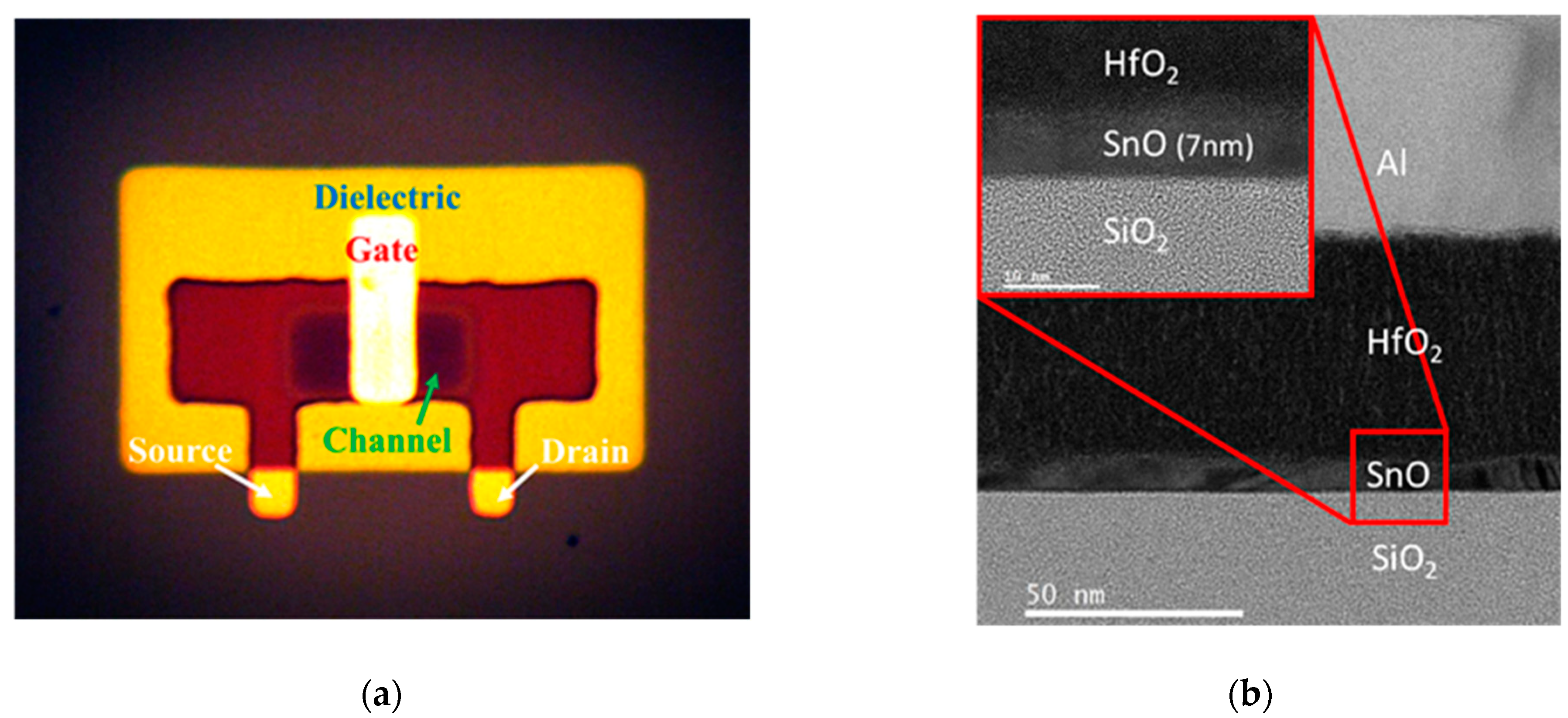
Figure 1a illustrates the top-view photograph of top-gate nanosheet SnO p-TFT, where the light-reflective Al metal-gate is on the top of the device. Figure 1b depicts the cross-sectional transmission electron microscope (TEM) image of the device structure with top Al-metal-gate, HfO2 gate-dielectric, and p-type channel SnO on SiO2 IMD. The thickness of Al, HfO2, and nanosheet SnO is 50, 50, and 7 nm, respectively.
The Opp is critical for top-gate nanosheet SnO p-TFT, where the SnO channel was made by sputtering from a metal Sn target under different Opp conditions. This is because the SnO can be oxidized into oxygen-rich SnO2 [16]. The Opp can be expressed as follows:
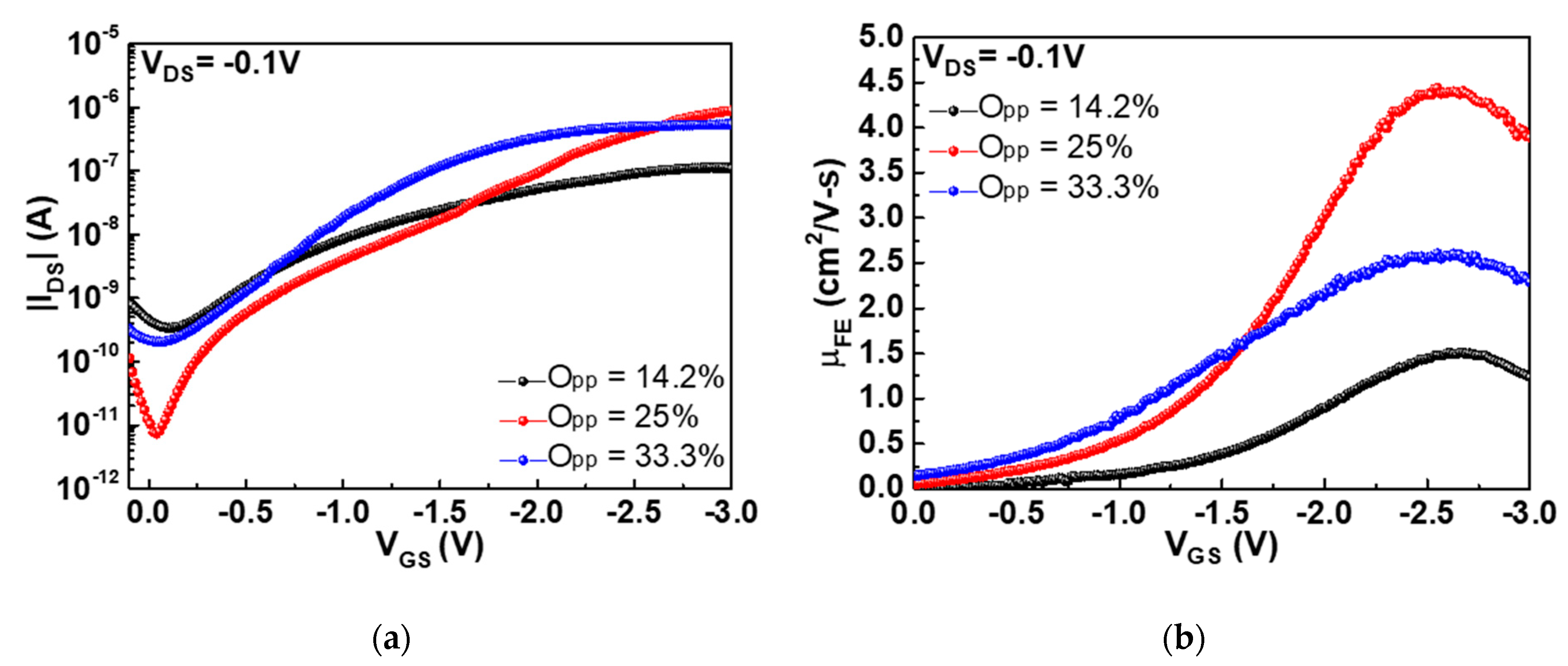
where and are the pressures of O2 and Ar in a sputtering system, respectively. For comparison, the Opp values were adjusted to 14.2%, 25% and 33.3% during sputtering. Figure 2a,b show the drain-source current versus gate-source voltage (|IDS|-VGS) and μFE-VGS characteristics of top-gate nanosheet SnO p-TFT devices, respectively, under different Opp values. The top-gate p-type SnO device exhibits the highest ION and the lowest leakage IOFF at the 25% Opp condition. The device with the best ION and IOFF is also consistent with the highest μFE. The μFE values were 1.5, 4.4 and 2.6 cm2/Vs at Opp of 14.2%, 25% and 33.3%, respectively. Here the μFE values were obtained at the standard and a small VDS of −0.1 V. Such abnormal μFE on Opp is ascribed to the following reasons. The device μFE increases with the increase in Opp from 14.2% to 25% due to the increased oxygen content in SnOx, with x ≤ 1, and device performance degrades at a high Opp of 33.3% owing to the formation of oxygen-rich SnOx, with x > 1. Under high Opp, SnOx becomes n-type electron-conductive SnO2 [12,13,14], which lowers the hole μFE under negative VGS.
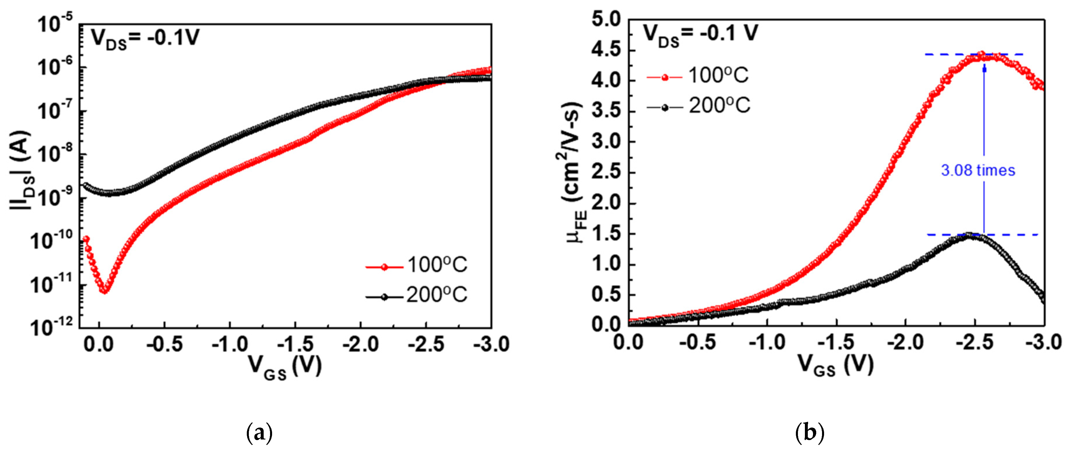
The device integrity in top-gate nanosheet SnO p-TFT is also dependent on HfO2 annealing temperature. To avoid plasma damage to the SnO channel layer, the high-κ HfO2 gate dielectric was deposited using an e-beam evaporator and subjected to post-annealing at 100 and 200 °C for 30 min under N2 ambient. Here the SnO layers were deposited under 25% Opp and annealed at 200 °C under N2 ambient. Subsequently, the HfO2 were deposited and annealed at 100 °C or 200 °C under the N2 ambient. The |IDS|-VGS and μFE-VGS characteristics of SnO p-TFTs with 100 and 200 °C post-annealing are shown in Figure 3a, b, respectively. The ION/IOFF and μFE values of the SnO p-TFT at 100 °C post-annealing are 1.2 × 10⁵ and 4.4 cm2/Vs, respectively, which are much better than those obtained at 200 °C: 4.6 × 10² and 1.44 cm2/Vs, respectively. The ION/IOFF is even better than previous bottom-gate SnO p-TFT [16] possibly due to the thinner SnO channel used in this study, which slightly degrades the μFE. A thin channel layer is needed to fully deplete the conductive oxide semiconductor SnO, similar to the low IOFF using ultra-thin body Si-on-Insulator (SOI) and Fin field-effect transistor (FinFET). However, the small sub-10 nm-scale channel thickness can increase the interface roughness scattering and decrease the mobility.
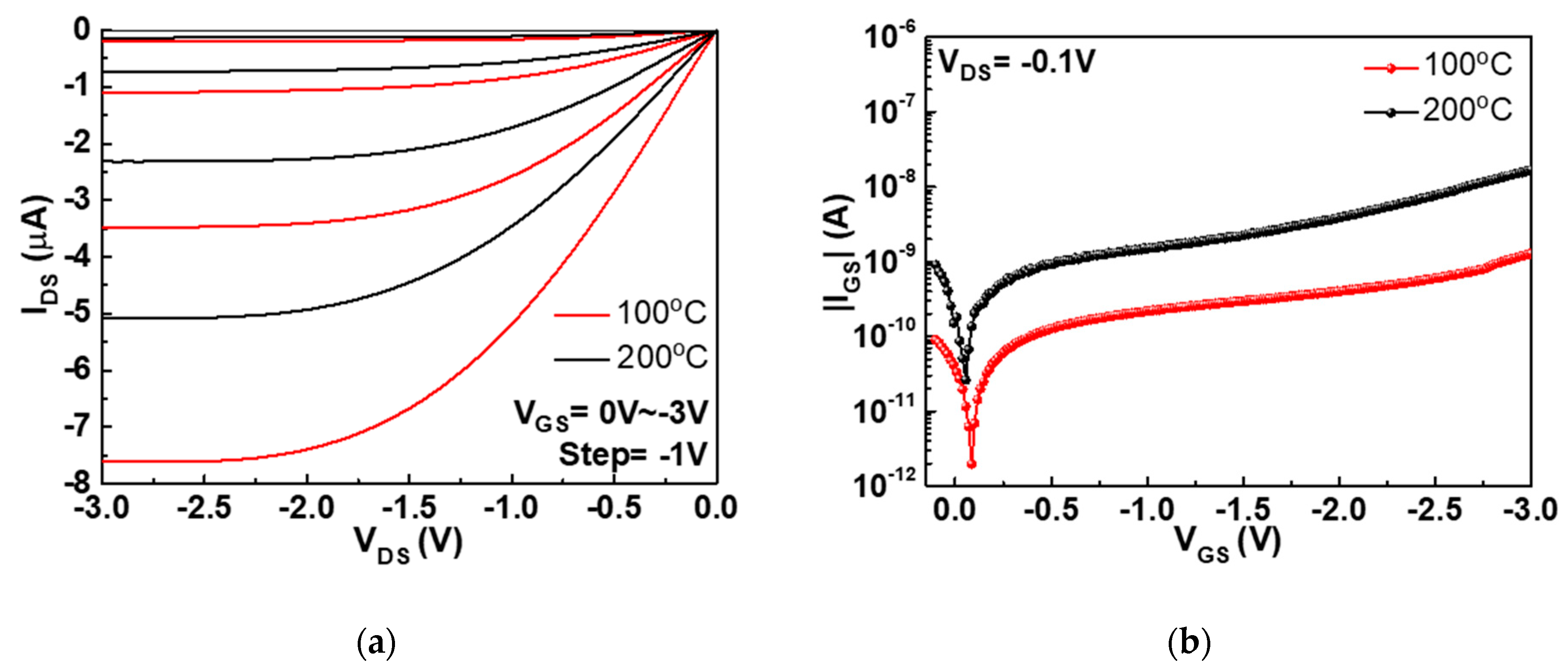
To investigate the mechanism of such annealing temperature dependence, Figure 4a,b plot the IDS versus drain-source voltage (IDS-VDS) and the gate-source current versus gate-source voltage (|IGS|-VGS) characteristics of top-gate SnO p-TFTs, respectively, at annealing temperatures of 100 and 200 °C. The p-TFT device at 100 °C annealing shows higher |IDS| than that at 200 °C annealing, corresponding to the higher μFE (Figure 3b). In normal case, a high post-annealing temperature of high-κ gate dielectric is necessary to reduce the gate leakage current and improve the device performance. However, the measured |IGS| of HfO2/SnO p-TFT annealed at 200 °C shows one order of magnitude higher gate leakage than that in the device annealed at 100 °C. The as-deposited HfO2 layer without annealing has too high gate leakage current due to defect conduction [41] and unsuitable for device application. To decrease the defect-conductive leakage current, even higher annealing temperature is required for metal-gate/high-κ/Si CMOS [39,42,43].
To further inspect the unusual annealing temperature dependence on device performance, material analysis of atomic force microscope (AFM), X-ray photoelectron spectroscopy (XPS), and secondary ion mass spectrometry (SIMS) were performed. In Figure S1, the surface roughness of the 50 nm HfO2 films annealed at 100 °C, 200 °C and 400 °C were analyzed through AFM. The root mean square values of surface roughness show slightly decrease along with the increasement of the annealing temperature. The HfO2 dielectric with different annealing temperatures were also analyzed by XPS. As shown in Figure S2, the binding energies of Hf-O and non-lattice O were 530 eV and 531.3 eV, respectively. The peak intensity of non-lattice O was related to the defects in HfO2 dielectric, which decreased with increasing post-annealing temperature. From the AFM and XPS analysis, the good device performance at 100 °C annealing is not related to the tiny difference of HfO2 layer.
To further investigate the Opp effect on chemical composition of the SnO layer, the XPS analyses on channel SnO were performed at the Opp of 14.2%, 25% and 33.3%. The HfO2 layer of HfO2/SnO stack were etched before the XPS analysis. The XPS data are depicted in Figure 5. The XPS spectra can be deconvolved into three curves from the Sn2+O, Sn4+O2 and Sn0 signals, with their corresponding energies of 486.8, 486 and 484.4 eV, respectively. The composition x values of SnOx deposited at Opp = 14.2%, 25% and 33.3% were 0.8, 0.95 and 1.3, respectively, which explains well the measured electrical data in Figure 2.
Figure 6a–c show the SIMS profiles of Hf, Sn and O atoms from the HfO2/SnO device structure annealed at 100, 200 and 400 °C, respectively. Increasing the annealing temperature from 100 to 400 °C led to significant Sn diffusion from SnO into HfO2. This is attributed to the weak Sn–O band enthalpy [38], even though it also leads to high hole mobility [15,16]:
SnO → Sn2+ + O2−
The charged Sn2+ can diffuse into HfO2, create vacancies at elevated temperatures, and, together with charged O2− ions, allow HfOx diffusion into the SnO layer at 200 °C annealing temperature. The inter-diffusion of Sn and Hf atoms and the formed vacancies and charged ions further degrade the HfO2 gate-dielectric and HfO2/SnO interface that cause poor |IGS|, μFE, ION, and IOFF. The amount of Hf diffusion into the SnO layer at 400 °C annealing temperature can be calculated by the area within SnO layer in Figure 6c, which is 1.15 times higher than the HfO2/SnO annealed at 200 °C. The Sn atoms diffused into HfO2 layer at 400 °C were 1.14 times more than the HfO2/SnO annealed at 200 °C. Thus, the higher post-annealing temperature will cause more inter-diffusion between HfO2 and SnO.
The diffused Sn2+ can behave as trap states in HfO2 gate dielectric, provide extra transport paths for the carriers, and lead to higher gate leakage current (Figure 4b). To understand the conduction mechanism of gate leakage current, the measured data were fitted with various mechanisms. As shown in Figure 7a, the measured |IGS|-VGS fits well with the hopping conduction [44,45,46,47], under an electric field (E) of <0.25 MV/cm, for 100 and 200 °C annealed top-gate SnO p-TFTs, where the slope of ln(|JGS|)-E is 5.72 and 4.91, respectively. The hopping conduction mechanism is expressed as [45]:
where J, q, a, n, ν, and Ea are the current density, electron charge, mean hopping distance, carrier concentration, thermal vibration frequency of carriers at trap states, and activation energy, respectively. The hopping distances of 100 and 200 °C annealed devices calculated from Equation (3) are 1.48 and 1.27 nm, respectively. The smaller hopping distance is ascribed to the Sn diffusion in HfO2, which increases the gate leakage JGS. The mechanism of poor gate leakage current and interface at high annealing temperature is depicted schematically in Figure 7b. The trap-induced hopping conduction causes high |IGS|. The degraded interface by Sn and Hf inter-diffusion and created vacancies increase the hole scattering from the source to drain, thus lowering the important ION and μFE. The created vacancies also increase the IOFF through defect conduction. The device performance can be further evaluated by the |IDS|-VGS hysteresis curves. The defect density formed by hysteresis curves, under forward and reverse sweep between 0 to −3 V, are 1.5 × 10¹² and 5.4 × 1012 cm−2 for device annealed at 100 and 200 °C, respectively. This result is consistent to our conclusion: the higher post-annealing temperature creates more defects in the HfO2/SnO gate capacitor, which leads to higher gate leakage current, lower hole mobility, and poorer hysteresis than the one annealed at lower 100 °C temperature.
The sub-threshold slope is related to interface trap, which can be calculated [48]:
where the Cdep, Cit and Cox are the depletion capacitance, interface trap capacitance and gate dielectric capacitance, respectively. The interface trap density (Dit) is 2.5 × 10¹³ eV−1cm−2 that is higher than the metal-gate/high-κ/Si CMOS. Therefore, the hump of sub-threshold |IDS|-VGS curve in Figure 2 is due to the charge modulation from the interface traps [49]. In comparison with SnO atomic density of 2.9 × 10²² atoms/cm3 or sheet atomic density of 9.4 × 10¹⁴ atoms/cm2, the Dit is only 2.7% of the sheet atoms of SnO. Thus, the electronic measurement is highly sensitive to defects compared with other measurements.
The μFE data increase to a peak value and decrease with increasing gate field. The detailed physical analysis in oxide semiconductor transistor is not reported yet. However, such hole mobility dependence is generally observed in SiO2/Si [50], high-κ/Si [51,52,53], SiO2/SiGe [54], high-κ/SiGe [55] and high-κ/Ge [56] p-MOSFETs. Because the Si, SiGe, Ge and SnO are all semiconductors and have the similar valance band structure, the decreased mobility at high electric field may be due to the similar mechanisms of phonon and interface roughness scatterings [57].
The La2O3 can achieve the excellent performance of low leakage current and high-κ value [55,58,59], but the moisture degradation is stronger than the HfO2 and ZrO2. The ZrO2 [60] has a higher κ value than HfO2 once crystallized, which is widely used for dynamic random-access memory (DRAM) capacitor. For gate dielectric application, orientation-independent amorphous material like conventional SiO2 is needed [61]. The TiO2 has the highest κ value but suffers from the small energy bandgap and high leakage current [62]. Thus, the TiO2 is generally added to other high-κ dielectric to increase the overall κ value [63]. The Al2O3 has been used for gate dielectric due to its excellent stability [40], but suffers from relatively lower κ value than HfO2. Therefore, the HfO2 is used for CMOS application and also for this work.
To inspect the stability of the top-gate SnO TFT devices, the devices were measured at as-fabricated and after retention in air ambient for two months, as depicted in Figure 8. In comparison with the conventional bottom-gate structure, such top-gate device shows huge stability improvement after retention in air [32], which is due to fully covered channel layer by metal-gate and gate-dielectric. Therefore, both the 100 and 200 °C annealed top-gate transistors show only slight degradation after exposure in air for two months. The top-gate HfO2/SnO p-TFT has slightly lower hole μFE of 4.4 cm2/Vs than our previously reported 7.6 cm2/Vs of bottom-gate HfO2/SnO device, which is attributed to the HfO2/SnO inter-diffusion. Because of the larger SS of top-gate device than the bottom-gate one with the same HfO2 and SnO, the HfO2/SnO interface degradation is confirmed from Equation (4).
Table 1 presents a comparison of the essential device characteristics of top-gate SnO p-TFTs [11,33,34,35] The merits of this work are the highest μFE of 4.4 cm2/Vs, largest ION/IOFF of 1.2 × 10⁵, and sharpest SS of 526 mV/decade reported to date at fabrication temperatures of only 100–200 °C. This device thus has high potential to be integrated into the IMD layer of Si chips for monolithic 3D and brain-mimicking IC applications.
4. Conclusions
While SnO has the advantage of high hole mobility, it also has low bond enthalpy. The key factor for good device integrity of top-gate HfO2/SnO p-TFT is to maintain the low process temperature, which can preserve good HfO2/SnO interface. Such a low-temperature fabrication (100–200 °C) and excellent device performance are crucial for monolithic 3D and brain-mimicking ICs made on the backend IMD layers of Si chips.
Supplementary Materials
The following are available online at https://0-www-mdpi-com.brum.beds.ac.uk/2079-4991/11/1/92/s1, Figure S1: The surface roughness analysis of HfO2 annealed at (a) 100 °C, (b) 200 °C and (c) 400 °C through AFM. Figure S2: The O1s spectra of HfO2 films annealed at (a) 100 °C, (b) 200 °C and (c) 400 °C.
Author Contributions
T.J.Y. did the experiments; A.C. is the principle investigator (PI) to monitor the project; V.G. is the co-PI for this work. All authors reviewed the manuscript. All authors have read and agreed to the published version of the manuscript.
Funding
This research was funded by Ministry of Science and Technology of Taiwan, project no. 107-2221-E-009-092-MY3.
Institutional Review Board Statement
Not applicable.
Informed Consent Statement
Not applicable.
Data Availability Statement
The data presented in this study are available on request from the corresponding author. The data are not publicly available due to privacy.
Acknowledgments
We would also like to thank Y. R. Wang for assisting the device fabrication during her master degree study.
Conflicts of Interest
The authors declare no conflict of interest.
References
- Fortunato, E.; Barquinha, P.; Martins, R. Oxide semiconductor thin-film transistors: A review of recent advances. Adv. Mater. 2012, 24, 2945–2986. [Google Scholar] [CrossRef] [PubMed]
- Nomura, K.; Ohta, H.; Takagi, A.; Kamiya, T.; Hirano, M.; Hosono, H. Room-temperature fabrication of transparent flexible thin-film transistors using amorphous oxide semiconductors. Nature 2004, 432, 488–492. [Google Scholar] [CrossRef] [PubMed]
- Su, N.C.; Wang, S.J.; Huang, C.C.; Chen, Y.H.; Huang, H.Y.; Chiang, C.K.; Chin, A. Low-voltage-driven flexible InGaZnO thin-film transistor with small subthreshold swing. IEEE Electron. Device Lett. 2010, 31, 680–682. [Google Scholar]
- Petti, L.; Munzenrieder, N.; Vogt, C.; Faber, H.; Buthe, L.; Cantarella, G.; Bottacchi, F.; Anthopoulos, T.D.; Troster, G. Metal oxide semiconductor thin-film transistors for flexible electronics. Appl. Phys. Rev. 2016, 3, 021303. [Google Scholar] [CrossRef] [Green Version]
- Shih, C.W.; Chin, A. Remarkably High mobility thin-film transistor on flexible substrate by novel passivation material. Sci. Rep. 2017, 7, 1147. [Google Scholar] [CrossRef] [PubMed] [Green Version]
- Yin, X.; Deng, S.; Li, G.; Zhong, W.; Chen, R.; Li, G.; Yeung, F.S.Y.; Wong, M.; Kwok, H.S. Low Leakage Current Vertical Thin-Film Transistors with InSnO-stabilized ZnO Channel. IEEE Electron. Device Lett. 2020, 41, 248–251. [Google Scholar] [CrossRef]
- Ohshima, H.; Morozumi, S. Future trends for TFT integrated circuits on glass substrates. In Proceedings of the International Technical Digest on Electron Devices Meeting, Washington, DC, USA, 3–6 December 1989. [Google Scholar]
- Liu, A.; Liu, G.; Zhu, H.; Song, H.; Shin, B.; Fortunato, E.; Martin, R.; Shan, F. Water-induced scandium oxide dielectric for low-operating voltage n- and p-type metal-oxide thin-film transistors. Adv. Funct. Mater. 2015, 25, 7180–7188. [Google Scholar] [CrossRef]
- Liang, L.Y.; Cao, H.T.; Chen, X.B.; Liu, Z.M.; Zhuge, F.; Luo, H.; Li, J.; Lu, Y.C.; Lu, W. Ambipolar inverters using SnO thin-film transistors with balanced electron and hole mobilities. Appl. Phys. Lett. 2012, 100, 263502. [Google Scholar] [CrossRef]
- Lee, C.H.; Sazonov, A.; Nathan, A. High mobility n-channel and p-channel nanocrystalline silicon thin-film transistors. In Proceedings of the IEEE International Electron Devices Meeting, IEDM Technical Digest, Washington, DC, USA, 5 December 2005. [Google Scholar]
- Nomura, K.; Kamiya, T.; Hosono, H. Ambipolar oxide thin-film transistor. Adv. Mater. 2011, 23, 3431–3434. [Google Scholar] [CrossRef]
- Shih, C.W.; Chin, A. New material transistor with record-high field-effect mobility among wide-band-gap semiconductors. ACS Appl. Mater. Interfaces 2016, 8, 19187–19191. [Google Scholar] [CrossRef] [Green Version]
- Shih, C.W.; Chin, A.; Lu, C.F.; Su, W.F. Remarkably high mobility ultra-thin-film metal-oxide transistor with strongly overlapped orbitals. Sci. Rep. 2016, 6, 19023. [Google Scholar] [CrossRef] [PubMed] [Green Version]
- Shih, C.W.; Yen, T.J.; Chin, A.; Lu, C.F.; Su, W.F. Low-temperature processed tin oxide transistor with ultraviolet irradiation. IEEE Electron. Device Lett. 2019, 40, 909–912. [Google Scholar] [CrossRef]
- Shih, C.W.; Chin, A.; Lu, C.F.; Yi, S.H. Extremely high mobility ultra-thin metal-oxide with ns2np2 configuration. In Proceedings of the 2015 IEEE International Electron Devices Meeting (IEDM), Washington, DC, USA, 7–9 December 2015; pp. 145–148. [Google Scholar]
- Shih, C.W.; Chin, A.; Lu, C.F.; Su, W.F. Remarkably high hole mobility metal-oxide thin-film transistors. Sci. Rep. 2018, 8, 889. [Google Scholar] [CrossRef] [PubMed] [Green Version]
- Chin, A.; Yen, T.J.; Shih, C.W.; Chen, Y.D. High mobility metal-oxide devices for display SoP and 3D brain-mimicking IC. Proc. Int. Disp. Workshops 2019, 26, 455–457. [Google Scholar] [CrossRef]
- Chin, A.; Chen, Y.D. Technologies toward three-dimensional brain-mimicking IC architecture. In Proceedings of the 2019 Electron Devices Technology and Manufacturing Conference (EDTM), Singapore, 12–15 March 2019; pp. 472–474. [Google Scholar]
- Kwon, J.; Takeda, Y.; Shiwaku, R.; Tokito, S.; Cho, K.; Jung, S. Three-dimensional monolithic integration in flexible printed organic transistors. Nat. Commun. 2019, 10, 54. [Google Scholar] [CrossRef] [Green Version]
- Sisman, Z.; Bolat, S.; Okyay, A.K. Atomic layer deposition for vertically integrated ZnO thin film transistors: Toward 3D High packing density thin film electronics. Phys. Status Solidi C 2017, 14, 1700128. [Google Scholar]
- Felfel, A.M.; Datta, K.; Dutt, A.; Veluri, H.; Zaky, A.; Thean, A.V.Y.; Aly, M.M.S. Quantifying the benefits of monolithic 3D computing systems enabled by TFT and RRAM. In Proceedings of the 2020 Design, Automation & Test in Europe Conference & Exhibition (DATE), Grenoble, France, 9–13 March 2020; pp. 43–48. [Google Scholar]
- Choi, S.H.; Jang, J.H.; Kim, J.J.; Han, M.K. Low-temperature organic (CYTOP) passivation for improvement of electric characteristics and reliability in IGZO TFTs. IEEE Electron. Device Lett. 2012, 33, 381–383. [Google Scholar] [CrossRef]
- Chowdhury, M.D.H.; Mativenga, M.; Um, J.G.; Mruthyunjaya, R.K.; Heiler, G.N.; Tredwell, T.J.; Jang, J. Effect of SiO2 and SiO2/SiNx passivation on the stability of amorphous indium–gallium zinc-oxide thin-film transistors under high humidity. IEEE Trans Electron. Devices 2015, 62, 869–874. [Google Scholar] [CrossRef]
- Park, J.; Song, I.; Kim, S.; Kim, S.; Kim, C.; Lee, J.; Lee, H.; Lee, E.; Yin, H.; Kim, K.K.; et al. Self-aligned top-gate amorphous gallium indium zinc oxide thin film transistors. Appl. Phys. Lett. 2008, 93, 053501. [Google Scholar] [CrossRef]
- King, T.J. Trends in polycrystalline-silicon thin-film transistor technology for AMLCD’s. In Proceedings of the Second International Workshop on Active Matrix Liquid Crystal Displays, Bethlehem, PA, USA, 25–26 September 1995; pp. 80–86. [Google Scholar]
- Wang, Z.; Nayak, P.K.; Caraveo-Frescas, J.A.; Alshareef, H.N. Recent developments in p-type oxide semiconductor materials and devices. Adv. Mater. 2016, 28, 3831–3892. [Google Scholar] [CrossRef] [Green Version]
- Caraveo-Frescas, J.A.; Nayak, P.K.; Al-Jawhari, H.A.; Granato, D.B.; Schwingenschlogl, U.; Alshareef, H.N. Record mobility in transparent p-type tin monoxide films and devices by phase engineering. ACS Nano 2013, 7, 5160–5167. [Google Scholar] [CrossRef] [PubMed]
- Batzill, M.; Diebold, U. The surface and materials science of tin oxide. Prog. Surf. Sci. 2005, 79, 47–154. [Google Scholar] [CrossRef]
- Fortunato, E.; Barros, R.; Barquinha, P.; Figueiredo, V.; Park, S.H.K.; Hwang, C.S.; Rodrigo, M. Transparent p-type SnOx thin film transistors produced by reactive rf magnetron sputtering followed by low temperature annealing. Appl. Phys. Lett. 2010, 97, 052103–052105. [Google Scholar] [CrossRef]
- Pham, H.P.; Nguyen, T.H.Y.; Nguyen, A.H.T.; Vo, N.T.; Thuy, T.G.L.; Nguyen, H.H.; Hoa, H.T.M.; Tran, Q.T. Effects of substrate temperature on characteristics of the p-type Ag-doped SnOx thin films prepared by reactive DC magnetron sputtering. J. Photoch. Photobio. A Chem. 2020, 388, 112157. [Google Scholar] [CrossRef]
- Li, Y.; Xin, Q.; Du, L.; Qu, Y.; Li, H.; Kong, X.; Wang, Q.; Song, A. Extremely sensitive dependence of SnOx film properties on sputtering power. Sci. Rep. 2016, 6, 36183. [Google Scholar] [CrossRef] [Green Version]
- Yen, T.J.; Chin, A.; Gritsenko, V. High performance top-gate thin film transistor with an ultra-thin channel layer. Nanometerials 2020, 10, 2145. [Google Scholar] [CrossRef]
- Ogo, Y.; Hiramatsu, H.; Nomura, K.; Yanagi, H.; Kamiya, T.; Masahiro, H.; Hosono, H. P-channel thin-film transistor using p-type oxide semiconductor, SnO. Appl. Phys. Lett. 2008, 93, 032113. [Google Scholar] [CrossRef]
- Cheng, I.C.; Hsu, S.M.; Lin, W.C.; Chen, J.Z. Influence of mechanical bending strain on bias-stress stability of flexible top-gate p-type SnO TFTs. Proc. SPIE 2020, 11304, 1–6. [Google Scholar]
- Khan, M.A.; Caraveo-Frescas, J.A.; Alshareef, H.N. Hybrid dual gate ferroelectric memory for multilevel information storage. Org. Electron. 2015, 16, 9–17. [Google Scholar] [CrossRef]
- Hautier, G.; Miglio, A.; Ceder, G.; Rignanese, G.-M.; Gonze, X. Identification and design principles of low hole effective mass p-type transparent conducting oxides. Nat. Commun. 2013, 4, 2292. [Google Scholar] [CrossRef] [Green Version]
- Nakano, Y.; Saeki, S.; Morikawa, T. Optical bandgap widening of p-type Cu2O films by nitrogen doping. Appl. Phys. Lett. 2009, 94, 022111. [Google Scholar] [CrossRef] [Green Version]
- Wu, C.H.; Hung, B.F.; Chin, A.; Wang, S.J.; Chen, W.J.; Wang, X.P.; Li, M.F.; Zhu, C.; Jin, Y.; Tao, H.J.; et al. High temperature stable [Ir3Si-TaN]/HfLaON CMOS with large work-function difference. In Proceedings of the 2006 International Electron Devices Meeting, San Francisco, CA, USA, 11–13 December 2006; pp. 617–620. [Google Scholar]
- Zhu, S.; Yu, H.Y.; Whang, S.J.; Chen, J.H.; Shen, C.; Zhu, C.; Lee, S.J.; Li, M.F.; Chan, D.S.H.; Yoo, W.J.; et al. Schottky-barrier S/D MOSFETs with high-κ gate dielectrics and metal gate electrode. IEEE Electron. Device Lett. 2004, 25, 268–270. [Google Scholar] [CrossRef]
- Zhu, S.; Li, R.; Lee, S.J.; Li, M.F.; Du, A.; Singh, J.; Zhu, C.; Chin, A.; Hwong, D.L. Germanium pMOSFETs with Schottky-barrier Germanide S/D, high-κ gate dielectric and metal gate. IEEE Electron. Device Lett. 2005, 26, 81–83. [Google Scholar]
- Islamov, D.R.; Gritsenko, V.A.; Rzhanov, A.V.; Cheng, C.H.; Chin, A. Bipolar conductivity in amorphous HfO2. Appl. Phys. Lett. 2001, 99, 072109. [Google Scholar] [CrossRef] [Green Version]
- Chin, A.; Liao, C.C.; Lu, C.H.; Chen, W.J.; Tsai, C. Device and reliability of high-κ Al2O3 gate dielectric with good mobility and low Dit. VLSI Symp. Tech. Digest. 1999, 135–136. [Google Scholar] [CrossRef]
- Cheng, C.F.; Wu, C.H.; Su, N.C.; Wang, S.J.; McAlister, S.P.; Chin, A. Very low Vt [Ir-Hf]/HfLaO CMOS using novel self-aligned low temperature shallow junctions. In Proceedings of the 2007 IEEE International Electron Devices Meeting, Washington, DC, USA, 10–12 December 2007; pp. 333–336. [Google Scholar]
- Wang, Z.; Yu, H.; Tran, X.A.; Fang, Z.; Wang, J.; Su, H. Transport properties of HfO2-x based resistive-switching memories. Phys. Rev. B 2012, 85, 195322. [Google Scholar] [CrossRef]
- Chiu, F. A review on conduction mechanisms in dielectric films. Adv. Mater. Sci. Eng. 2014, 2014, 578168. [Google Scholar] [CrossRef] [Green Version]
- Shaposhnikov, A.V.; Perevalov, T.V.; Gritsenko, V.A.; Cheng, C.H.; Chin, A. Mechanism of GeO2 resistive switching based on the multi-phonon assisted tunneling between traps. Appl. Phys. Lett. 2012, 100, 243506. [Google Scholar] [CrossRef] [Green Version]
- Yen, T.J.; Chin, A.; Gritsenko, V. High performance all nonmetal SiNx resistive random access memory with strong process dependence. Sci. Rep. 2020, 10, 2807. [Google Scholar] [CrossRef] [Green Version]
- Chang, M.F.; Lee, P.T.; McAlister, S.P.; Chin, A. Low sub-threshold swing HfLaO/Pentacene oganic thin film transistors. IEEE Electron. Device Lett. 2008, 29, 215–217. [Google Scholar] [CrossRef]
- Lee, H.J.; Abe, K.; Noh, H.Y.; Kim, J.S.; Lee, H.; Lee, M.L. Analysis of the hump phenomenon and needle defect states formed by driving stress in the oxide semiconductor. Sci. Rep. 2019, 9, 11977. [Google Scholar] [CrossRef] [PubMed]
- Yu, D.S.; Wu, C.H.; Huang, H.C.; Chin, A.; Chen, W.J.; Zhu, C.X.; Li, M.F.; Kwong, D.L. Fully silicided NiSi and germanided NiGe dual gates on SiO2 n- and p-MOSFETs. IEEE Electron. Device Lett. 2003, 24, 739–741. [Google Scholar] [CrossRef]
- Wu, C.H.; Hung, B.F.; Chin, A.; Wang, S.J.; Wang, X.P.; Li, M.F.; Zhu, C.; Yen, F.Y.; Hou, Y.T.; Jin, Y.; et al. High-temperature stable HfLaON p-MOSFETs with high-work-function Ir3Si gate. IEEE Electron. Device Lett. 2007, 28, 292–294. [Google Scholar] [CrossRef]
- Lin, S.H.; Cheng, C.H.; Chen, W.B.; Yeh, F.S.; Chin, A. Low-threshold-voltage TaN/Ir/LaTiO p-MOSFETs incorporating low-temperature-formed shallow junctions. IEEE Electron. Device Lett. 2009, 30, 681–683. [Google Scholar] [CrossRef]
- Chang, M.F.; Lee, P.T.; Chin, A. Low-threshold-voltage MoN/HfAlO/SiON p-MOSFETs with 0.85-nm EOT. IEEE Electron. Device Lett. 2009, 30, 861–863. [Google Scholar] [CrossRef]
- Wu, Y.H.; Chin, A. High temperature formed SiGe p-MOSFETs with good device characteristics. IEEE Electron. Device Lett. 2000, 21, 350–352. [Google Scholar] [CrossRef] [Green Version]
- Huang, C.H.; Chen, S.B.; Chin, A. La2O3/Si0.3Ge0.7 p-MOSFETs with high hole mobility and good device characteristics. IEEE Electron. Device Lett. 2002, 23, 710–712. [Google Scholar] [CrossRef]
- Yu, D.S.; Huang, C.H.; Chin, A.; Zhu, C.; Li, M.F.; Cho, B.J.; Kwong, D.L. Al2O3/Ge-On-Insulator n- and p-MOSFETs with Fully NiSi and NiGe Dual Gates. IEEE Electron. Device Lett. 2004, 25, 138–140. [Google Scholar] [CrossRef]
- Takagi, S.; Toriumi, A.; Iwase, M.; Tango, H. On the universality of inversion layer mobility in Si MOSFET’s: Part I-effects of substrate impurity concentration. IEEE Trans. Electron. Device 1994, 41, 2357–2362. [Google Scholar] [CrossRef]
- Lin, C.Y.; Yu, D.S.; Chin, A.; Zhu, C.; Li, M.F.; Kwong, D.L. Fully silicided NiSi gate on La2O3 MOSFETs. IEEE Electron. Device Lett. 2003, 24, 348–350. [Google Scholar] [CrossRef]
- Wu, Y.H.; Yang, M.Y.; Chin, A.; Chen, W.J. Electrical characteristics of high quality La2O3 dielectric with equivalent oxide thickness of 5Å. IEEE Electron. Device Lett. 2000, 21, 341–343. [Google Scholar] [CrossRef] [Green Version]
- Tsai, C.Y.; Chiang, K.C.; Lin, S.H.; Hsu, K.C.; Chi, C.C.; Chin, A. Improved capacitance density and reliability of High-κ Ni/ZrO2/TiN MIM capacitors using laser annealing technique. IEEE Electron. Device Lett. 2010, 31, 749–752. [Google Scholar] [CrossRef]
- Chin, A.; Lin, B.C.; Chen, W.J.; Lin, Y.B.; Tsai, C. The effect of native oxide on thin gate oxide integrity. IEEE Electron. Device Lett. 1998, 19, 426–428. [Google Scholar] [CrossRef] [Green Version]
- Chiang, K.C.; Chin, A.; Lai, C.H.; Chen, W.J.; Cheng, C.F.; Hung, B.F.; Liao, C.C. Very high κ and high density TiTaO MIM capacitors for analog and RF applications. In Proceedings of the Digest of Technical Papers 2005 Symposium on VLSI Technology, Kyoto, Japan, 14–16 June 2005; pp. 62–63. [Google Scholar]
- Lin, S.H.; Chiang, K.C.; Chin, A.; Yeh, F.S. High density and low leakage current MIM capacitor using stacked TiO2/ZrO2 insulators. IEEE Electron. Device Lett. 2009, 30, 715–717. [Google Scholar] [CrossRef]
Figure 1.
(a) top-view photograph and (b) cross-sectional TEM image of the top-gate nanosheet SnO p-TFT device. The “white”-color gate on top of the device is due to the light-reflective Al metal.
Figure 1.
(a) top-view photograph and (b) cross-sectional TEM image of the top-gate nanosheet SnO p-TFT device. The “white”-color gate on top of the device is due to the light-reflective Al metal.

Figure 2.
(a) |IDS|-VGS and (b) μFE-VGS characteristics of top-gate nanosheet SnO p-TFTs with SnO channel deposited at different Opp conditions. The SnO layer was annealed at 200 °C and HfO2 layer was annealed at 100 °C.
Figure 2.
(a) |IDS|-VGS and (b) μFE-VGS characteristics of top-gate nanosheet SnO p-TFTs with SnO channel deposited at different Opp conditions. The SnO layer was annealed at 200 °C and HfO2 layer was annealed at 100 °C.

Figure 3.
(a) |IDS|-VGS and (b) μFE-VGS characteristics of top-gate nanosheet SnO TFT annealed at 100 °C N2 ambient and 200 °C N2 ambient.
Figure 3.
(a) |IDS|-VGS and (b) μFE-VGS characteristics of top-gate nanosheet SnO TFT annealed at 100 °C N2 ambient and 200 °C N2 ambient.

Figure 4.
(a) IDS-VDS and (b) |IGS|-VGS characteristics of top-gate nanosheet SnO TFTs annealed at 100 and 200 °C.
Figure 4.
(a) IDS-VDS and (b) |IGS|-VGS characteristics of top-gate nanosheet SnO TFTs annealed at 100 and 200 °C.

Figure 5.
The Sn 3d5/2 spectra of SnO films deposited at Opp of (a) 14.2%, (b) 25% and (c) 33.3%.

Figure 6.
SIMS depth profiles of HfO2/SnO stack annealed at (a) 100, (b) 200 and (c) 400 °C N2 ambient.
Figure 6.
SIMS depth profiles of HfO2/SnO stack annealed at (a) 100, (b) 200 and (c) 400 °C N2 ambient.

Figure 7.
(a) |IGS|-VGS characteristics of top-gate nanosheet HfO2/SnO p-TFTs annealed at 100 and 200 °C. (b) Schematic diagram to show gate leakage and inter-diffusion of top-gate SnO TFT device annealed at 200 °C.
Figure 7.
(a) |IGS|-VGS characteristics of top-gate nanosheet HfO2/SnO p-TFTs annealed at 100 and 200 °C. (b) Schematic diagram to show gate leakage and inter-diffusion of top-gate SnO TFT device annealed at 200 °C.

Figure 8.
The |IDS|-VGS characteristics of the top-gate nanosheet SnO TFT devices with (a) SnO deposited at Opp = 14.2% and HfO2 annealed at 100 °C, (b) SnO deposited at Opp = 25% and HfO2 annealed at 100 °C, (c) SnO deposited at Opp = 33.3% and HfO2 annealed at 100 °C, and (d) SnO deposited at Opp = 25% and HfO2 annealed at 200 °C. The devices were measured at as-fabricated and after 2 months’ exposure to air ambient.


Table 1.
The device performances of various top-gate SnO p-TFTs.
| Reference | SnO Thickness (nm) | Gate Insulator Materials | μFE (cm2/V·s) @VDS (V) | ION/IOFF | SS (mV/Decade) | Process Temp. (°C) |
|---|---|---|---|---|---|---|
| 11 | 15.4 | Y2O3 | 0.05 @-1 | 102 | - | 250 |
| 33 | 20 | Al2O3 | 1.3 @-2 | 102 | 7 | 575 |
| 34 | 15 | HfO2 | 0.71 @-1 | 1.6 × 10³ | 1.6 | 200 |
| 35 | 30 | P(VDF-TrFE) | 2.7 @-1 | 2.2 × 10² | 4 | 200 |
| This work | 7 | HfO2 | 4.4 @-0.1 | 2 × 10⁵ | 0.526 | 200 |
Publisher’s Note: MDPI stays neutral with regard to jurisdictional claims in published maps and institutional affiliations. |
© 2021 by the authors. Licensee MDPI, Basel, Switzerland. This article is an open access article distributed under the terms and conditions of the Creative Commons Attribution (CC BY) license (http://creativecommons.org/licenses/by/4.0/).
Share and Cite
MDPI and ACS Style
Yen, T.J.; Chin, A.; Gritsenko, V. Exceedingly High Performance Top-Gate P-Type SnO Thin Film Transistor with a Nanometer Scale Channel Layer. Nanomaterials 2021, 11, 92. https://0-doi-org.brum.beds.ac.uk/10.3390/nano11010092
AMA Style
Yen TJ, Chin A, Gritsenko V. Exceedingly High Performance Top-Gate P-Type SnO Thin Film Transistor with a Nanometer Scale Channel Layer. Nanomaterials. 2021; 11(1):92. https://0-doi-org.brum.beds.ac.uk/10.3390/nano11010092
Chicago/Turabian StyleYen, Te Jui, Albert Chin, and Vladimir Gritsenko. 2021. "Exceedingly High Performance Top-Gate P-Type SnO Thin Film Transistor with a Nanometer Scale Channel Layer" Nanomaterials 11, no. 1: 92. https://0-doi-org.brum.beds.ac.uk/10.3390/nano11010092
Note that from the first issue of 2016, this journal uses article numbers instead of page numbers. See further details here.