1. Introduction
The γ-phase of copper iodide (CuI) with a direct bandgap (
Eg) of ≈3.1 eV has been attracting increased attention as an emergent transparent
p-type semiconductor with a high hole mobility (
μh); for example, the
μh value reaches up to ≈44 cm
2V
−1s
−1 in a single crystal, thereby being higher than that of any other conventional
p-type oxides [
1]. Even in a thin film form, CuI exhibits a relatively high
μh of typically 6–7 cm
2V
−1s
−1 at a hole concentration (
p) of ≈10
19 cm
−3 [
2]. Moreover, with the additional heat treatment such as ex situ thermal annealing [
3] or in situ thermal annealing during deposition [
4],
μh values of those films are further enhanced more up to ≈26 cm
2V
−1s
−1. Such thermal annealing processes are known to suppress not only Cu vacancy (
VCu), which is the main source of acceptor in the CuI system, but also structural defects such as pinholes or grain boundaries. In this respect, the CuI thin films with proper heat treatment can play an important role of being a transparent
p-type layer in various optoelectronic devices such as solar cells [
5], a light-emitting diode [
6], a field-effect transistor [
7], and a UV photodetector [
8,
9].
In order to realize a transparent
pn diode based on the CuI, we have been investigating various heterojunction diodes made of
p-CuI and
n-type semiconductors [
2,
8,
9,
10,
11]; in our previous work, we have reported a transparent diode made of
p-CuI/
n-BaSnO
3−δ (BSO) films and its carrier transport behavior [
12]. The realized
p-CuI/
n-BSO diode exhibited a high current rectification ratio (
IF/
IR) of 6.75 × 10
5 at an external voltage bias of ±2 V. On the other hand, a high-quality BSO film often requires an epitaxial growth on a proper substrate such as SrTiO
3 (001), and its ideal growth temperature is rather high (≈800 °C). Therefore, for the applications in e.g., flexible UV photodetectors, it is desirable to test a heterojunction diode made of an alternative
n-type film that can be grown at a relatively low-temperature condition comparable to that of the CuI film and without the constraint of epitaxy.
Along this line of reasoning, Yamada et al. have recently reported that a heterojunction diode made of
p-CuI film and the well-known
n-type amorphous semiconductor InGaZnO (IGZO) film exhibits a high rectification ratio of ≈10
9 [
8]. Independent of this promising approach, we have been focusing on a new
n-type amorphous semiconductor SiZnSnO (SZTO) film that exhibits a high optical gap
Eg larger than 3.7 eV [
13] and a field-effect mobility of ≈38 cm
2V
−1s
−1 [
14]. It has been found that the
n-type SZTO film maintains enhanced electrical stability as compared to the IGZO film [
13], which is possibly due to reduced oxygen vacancies as controlled by Si concentration via strong Si–O bonding [
15]. In addition, the
n-type SZTO film has another advantage of being composed of non-toxic and abundant elements of Si and Sn. Therefore, we decided to adopt the SZTO as a transparent
n-type layer to realize a new heterojunction diode with the
p-CuI film.
Another potential merit of the
p-CuI/
n-SZTO diode lies in the capability of tuning the electronic energy diagram of the
n-type amorphous ZnSnO layer by the control of Si concentration. Such a capability might provide an opportunity for improving the efficiency of a potential optoelectronic device such as a light-emitting diode. As an example, Baek et al. [
6] have shown that the performance of the light-emitting diode made of
p-CuI/
n-Mg
xZn
1−xO quantum dot (
x = 0, 2.7, and 6 at %) has improved when the energy level difference between
n-Mg
xZn
1−xO and Al electrode is adjusted via the control of
x. The imbalance between the injected hole and electron carriers at the interface of a light-emitting diode can potentially lead to the decreased device performance. Thus, the control of electron and hole injection ratios via a proper tuning of energy band diagram can be an effective way to improve performance of the given light-emitting diode.
Yet another promising application direction of the
p-CuI/
n-SZTO diode is a self-powered UV photodetector [
16]. Recently, the photo-response of various
pn diode structures made of
p-CuI films (or nanoparticles) and various
n-type materials are widely being tested; those
n-type materials include IGZO films [
8], CsPbBr
3 crystals [
9], ZnO:Au films [
17], and ZnO films [
18], and β-Ga
2O
3 single crystals [
19]. Once realized, those photodetectors made of the
pn diode are expected to have self-powered characteristics and reliable responsivity under UV light illumination [
8,
9,
17,
18]. Thus, the diode made of
p-CuI and
n-SZTO can be another promising platform for realizing a flexible, transparent UV photodetector with a capability of tuning electronic band diagram in the SZTO layer. To realize such a device, quantitative understandings on the diode performance and energy band alignment at the interface should be prerequisite.
With the above motivations, we here report the realization of transparent heterojunction diodes made of novel transparent polycrystalline p-CuI film and amorphous n-SZTO film that has resulted in a high rectification ratio IF/IR of ≈107. To investigate the diode characteristics, various diode parameters, such as ideality factor, reverse saturation current, and series resistance, etc., are estimated from the diode curve fitting based on the Shockley diode equation. We propose an energy band diagram of the p-CuI/n-SZTO diode exhibiting type-II heterojunction and attribute the high rectification ratio to the improved transport properties of the CuI film, resulting from reduced ionized impurity scattering of Cu vacancies and enhanced diode interface via reduced structural defects. Our results show that the diode made of p-CuI/n-SZTO films exhibits an excellent electrical performance as a transparent pn diode with potential tunability of the energy band diagram, which can be useful for realizing flexible, cost-effective optoelectronic devices such as UV photodetectors and light-emitting diodes.
3. Results and Discussion
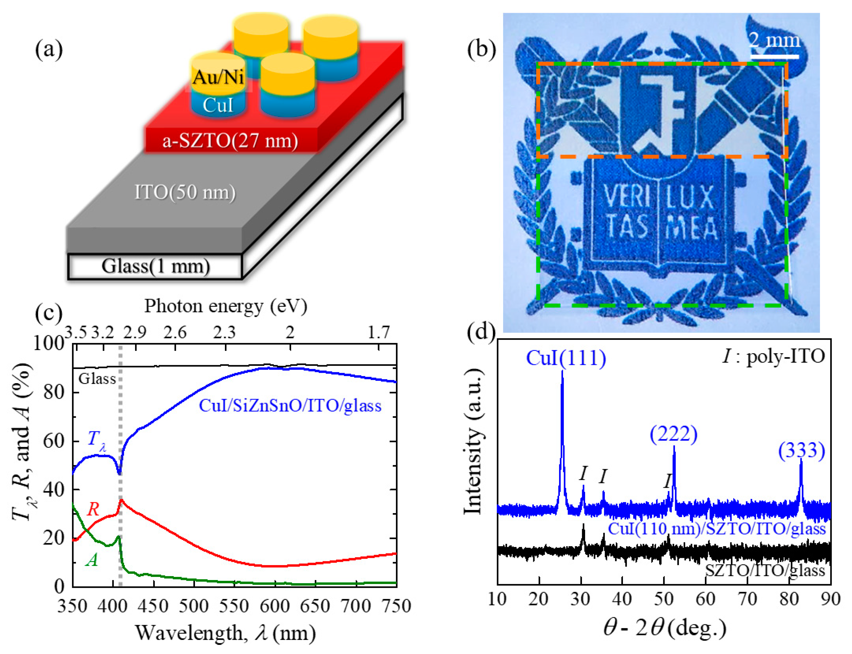
Figure 1a shows a schematic structure of the fabricated
p-CuI/
n-SZTO diode for electrical measurements, in which the SZTO film is grown on the ITO/glass, followed by the subsequent deposition of the circular CuI film and the metallic (Au/Ni) electrode.
Figure 1b is an actual photograph of the CuI/SZTO/ITO/glass film without the Au/Ni layer, demonstrating that all the layers are transparent in the visible spectral range. The CuI/SZTO films (the orange dashed line) were deposited with a lateral size of 10 × 4 mm
2 on the ITO/glass substrate (the green dashed line); the thicknesses of the CuI, the SZTO, and the ITO films are 110, 27, and 50 nm, respectively. Hereafter, we denote the term CuI (
x nm) as
x nm-thick CuI film where
x represents the thickness of the CuI film (
tCuI).
Figure 1c exhibits the optical transmittance (
Tλ), reflectance (
R), and absorption (
A) spectra as a function of wavelength
λ for the CuI/SZTO/ITO/glass (
Figure 1b), and a black solid line represents
Tλ of a bare glass substrate. The absorbance is obtained from the relationship of
A = 100−
Tλ−
R, exhibiting small values less than 5% at
λ ≥ 450 nm. The maximum
Tλ of the CuI/SZTO/ITO/glass is indeed found to be as high as ≈90% and is always larger than ≈80% in the visible spectral region (500–750 nm). In addition, the transmittance of the glass substrate
Tλ,glass is a nearly constant of ≈0.9 (the black solid line). According to the relationship of
Tλ,film =
Tλ,measured/
Tλ,glass,
Tλ,film of the remaining films (CuI/SZTO/ITO) is then likely to be higher than ≈88% in the visible spectral region. All these results quantitatively demonstrate why the fabricated diode structure (CuI/SZTO/ITO/glass) maintains optical transparency, as shown in
Figure 1b.
In addition, it is noteworthy that an exciton absorption peak is found at 407 nm (3.05 eV) (a gray dotted line in
Figure 1c), as frequently observed in the CuI film [
2,
4,
10,
12]. Then,
Eg of the CuI film is estimated as ≈3.1 eV from the relationship of
Eg =
EZ1,2 +
Eex where
EZ1,2 is an exciton absorption energy of CuI and
Eex is an exciton binding energy of 62 meV [
20]. The obtained
Eg value is similar to our previous result (≈3.08 eV) [
12] and other reports [
2,
3,
4]. Based on the observation of the similar optical bandgap, the optical spectra are likely to be expected as high enough regardless of
tCuI, as confirmed in the previous report [
12]. Furthermore, the observation of such a sharp exciton absorption peak supports that the as-grown CuI film is of high quality.
The crystallinity of the as-grown films (CuI/SZTO/ITO/glass substrate) has been investigated by the X-ray
θ-2
θ scan in
Figure 1d. The CuI film exhibits a preferred orientation along the (111) plane, similar to the CuI/glass sample case (see,
Figure S2 for the X-ray result). Since the nearest bottom layer is composed of an amorphous material, i.e., SZTO film or glass substrate, this (111) peak is unlikely to originate from the epitaxial CuI film [
12]. It is well-known that the CuI system exhibits randomly oriented in-plane domains within the CuI (111) plane due to the low surface stability energy of the (111) plane [
2]. The SZTO film cannot be identified in
Figure 1d due to its amorphous nature, as confirmed by our previous transmission electron microscopy and X-ray photoelectron spectroscopy studies [
21,
22]. The extra peaks are the polycrystalline ITO film denoted as a symbol of
I in
Figure 1d.
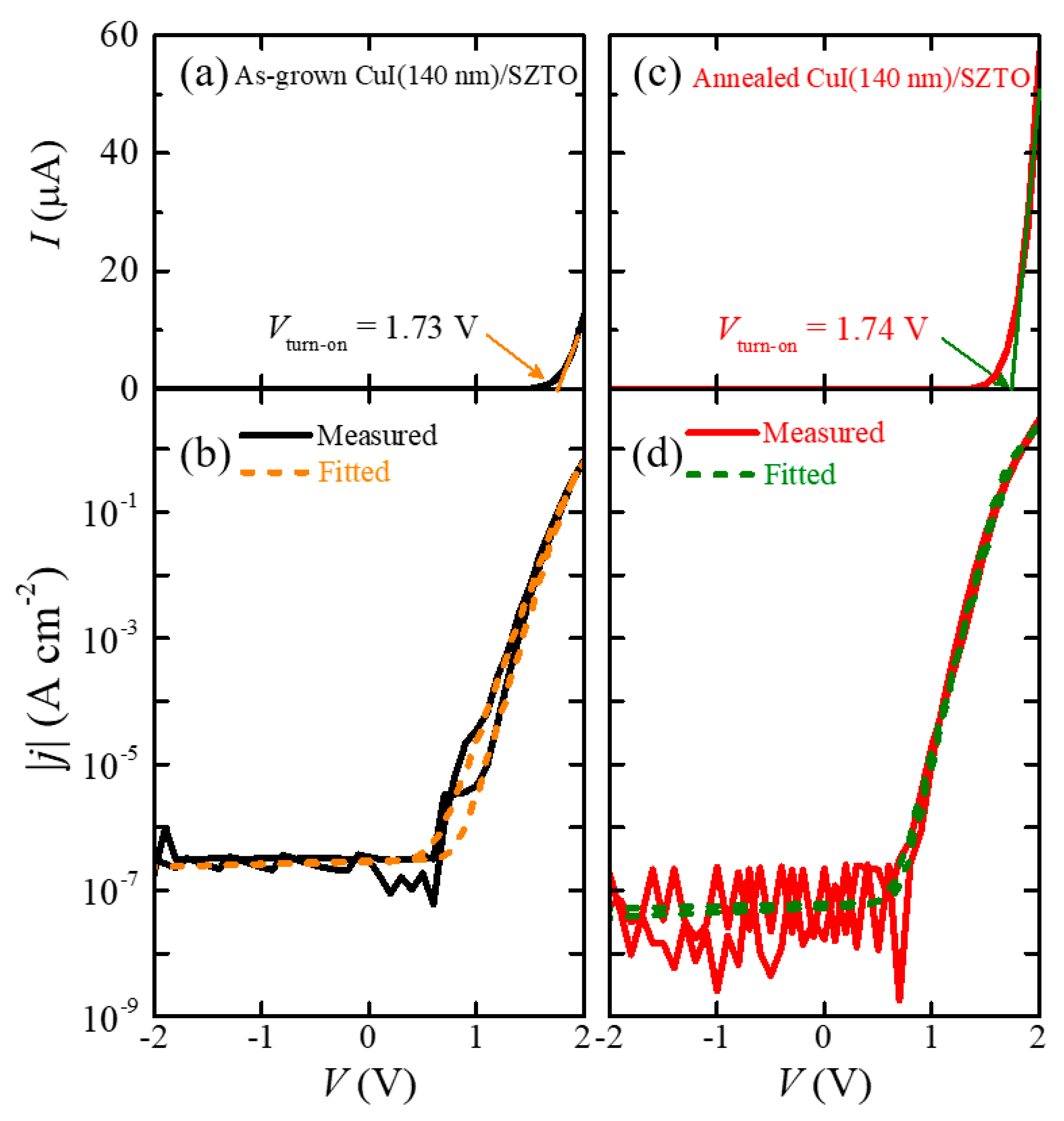
To investigate the electrical transport of the diodes before and after the N
2 annealing, we measured the
I-
V curves of the diodes, which have the structure shown in
Figure 1a using a two-point contact method. In this configuration, the two probe tips are connected to Au/Ni and ITO films for
p-CuI and
n-SZTO layers, respectively.
Figure 2a shows the
I-
V curve (black solid line) of the as-grown CuI (140 nm)/SZTO diode in a linear scale. A turn-on voltage (
Vturn-on), which is the on-set voltage for a large increase in the current level, has been determined from a linear extrapolation of the
I-
V curve in
Figure 2a. The estimated
Vturn-on of the as-grown diode was 1.73 V.
Figure 2b presents the corresponding |
j|-
V curve in a semi-log scale. To extract the quantitative information on the diode parameters, we have tried to fit the data with the Shockley diode equation in the full range from −2 V to +2 V:
where
Is is the reverse saturation current,
η is the ideality factor,
kB is the Boltzmann constant,
T is the absolute temperature,
Io is the offset current,
Rs is the series resistance, and
Rp is the parallel resistance [
11]. The orange lines in
Figure 2b represent the curve fitting results, which indeed well explain the measured data except for the irreversible charge trap effect near 0.8 V. We will discuss the resultant parameters in
Figure 3.
Similarly, the measured
I-
V and |
j|-
V curves in the annealed CuI (140 nm)/SZTO diode are plotted as red solid lines in
Figure 2c,d, respectively. The green dashed line of the |
j|-
V curve represents the curve fitting result. What is most conspicuous in the behavior of the annealed diode is the decrease (increase) of the current level in the negative (positive) bias region. This immediately points out that the current rectification ratio
IF/
IR, where
IF is the current value at +2 V and
IR is the current at −2 V, is enhanced after the annealing. As the SZTO layer is expected to be stable at the annealing condition (50 °C, 125 h), to understand the enhancement of
IF/
IR, one should understand first how the annealing process will affect the properties of CuI film. It is known that in the as-grown CuI film,
VCu is likely to exist, behaving as a dominant acceptor source and also as an ionized impurity scattering source. Upon the ex situ thermal annealing at 50 °C being performed for 125 h, iodine vacancies (
VI) can be additionally created, thereby compensating the native
VCu. In addition to
VCu compensation by
VI, thermal energy can provide extra energy for rendering the migration of existing Cu vacancies from the inside of the CuI film to the outside of the surface or grain boundary [
3]. Therefore, the optimal thermal annealing can lead to suppression of ionized impurity scattering via the compensation of
VCu by
VI and also by the reduction of
VCu inside the CuI film. At the same time, a reduction of structural defects near the grain boundaries of the CuI film is also expected, which in turn can form a smooth and uniform interface to improve the
pn diode performance. Reduced grain boundaries after annealing can be verified in the AFM image of the CuI film/glass in
Figure S3.
Several pieces of evidence supporting improved diode performance after annealing can be found in the
I-
V (or |
j|-
V) characteristics in
Figure 2c,d; the hysteresis of the |
j|-
V curve between the forward and reverse sweeping directions decreases,
Vturn-on slightly increases from 1.73 to 1.74 V, the offset current
Io decreases in the flat range from −2 to +0.7 V, and the |
j|-
V curve produces significant noise in the flat region. To better understand microscopically how the diode performance improves, we discuss here the supporting evidence in more detail. First, it should be reminded that irreversible charge traps mainly cause the diode hysteresis because the charged trap sites, such as
VCu, act as a slowly responding component under external voltage bias. Thus, the decreased hysteresis in the |
j|-
V curve demonstrates that the charged trap sites have been greatly reduced.
Second, the slight increase of
Vturn-on from 1.73 to 1.74 V also supports the improved diode performance. A threshold voltage (
Vth), which is an ideal voltage to begin the current flow, is expected to become fairly high in this diode; it is expressed by
Vth-p =
Vbi + |∆
EV/
e| for a
p-type carrier and by
Vth-n =
Vbi + |∆
EC/
e| for an
n-type carrier, where
Vbi is the built-in potential of a diode, ∆
EV is the valence band offset, and ∆
EC is the conduction band offset between two semiconductors [
2]. Based on the band diagram of the CuI/SZTO diode (vide infra, Figure 5), it turns out to be
Vbi = 0.99 V, |∆
EV/
e| = 2.55 V, and |∆
EC/
e| = 1.90 V, resulting in
Vth-p = 3.54 V for the injection of holes from
p-CuI to
n-SZTO and
Vth-n = 2.89 V for the injection of electrons from
n-SZTO to
p-CuI. Thus, it is likely that electron injection is more probable than hole injection because the absolute conduction band offset |∆
EC/
e| is 0.66 V less than |∆
EV/
e|. The obtained
Vturn-on = 1.74 V in
Figure 2c for the annealed diode is obviously smaller than the predicted
Vth-n = 2.89 V. Since the
VCu creates an intermediate state that can form an additional current path at the diode interface, the actual
Vturn-on should be lower than
Vth in general. Therefore, in turn, the increased
Vturn-on after annealing indicates reduced extra leakage current paths by the decrease of
VCu or by the compensation of
VCu.
Finally, the reduced
Io after annealing also supports the improved diode performance.
Io can be generated by other leakage sources irrelevant to the bias voltage such as instrumental effects or pinholes that can exist across two electrodes. Once
Io was formed at a diode, it appears as a constant current in the flat region of the |
j|-
V curve; for instance, the
Io level is ≈5.9 pA in the bias range from −2 to +0.7 V in
Figure 2b. Therefore, the reduced
Io level from 5.9 to 1.1 pA after the annealing in
Figure 2d indicates that such a side effect has been mitigated by the annealing, too. As the
Io decreased after annealing, the current noise in the negative bias range concurrently increased. It implies that the actual current is small enough to reach the resolution limit of the instrument (Keithley 4200-SCS, ±1 pA).
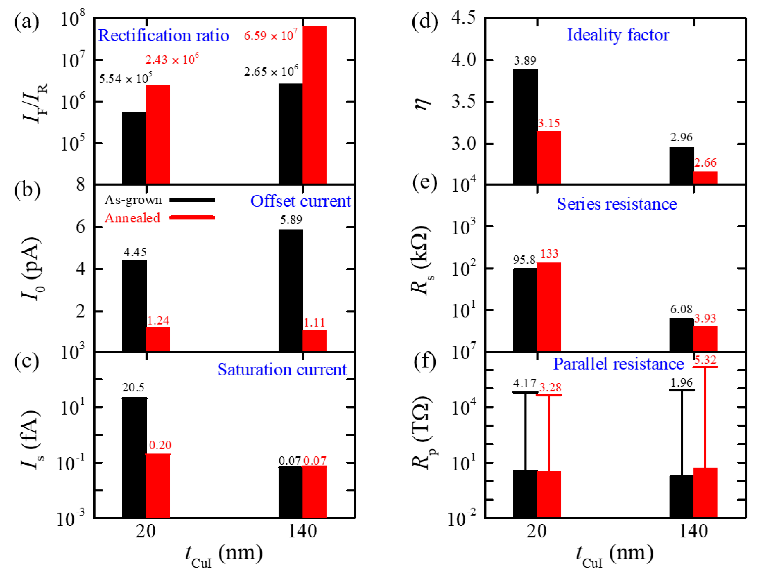
Figure 3 compares all the obtained diode parameters for both CuI (20 nm)/SZTO and CuI (140 nm)/SZTO diodes before and after annealing. Here, we remind the physical meaning of each diode parameter except for
IF/
IR and
Io already explained above.
Is represents the reverse saturation current, which occurs by the minority carriers located at the depletion region of a
pn diode.
η describes a diode transport model;
η is known to change by diffusion (
η = 1), recombination (
η = 2), and numerous defects region (
η > 2).
Rs is determined by the contact resistance of several junctions between two films and between the electrode/film, and
Rp represents the parasitic parallel resistance formed by an additional leakage path. In the case of the CuI (140 nm)/SZTO diode, the annealing process results in the increase of
IF/
IR from 2.7 × 10
6 to 6.6 × 10
7 by ≈25 times, the decrease of
Io from 5.9 to 1.1 pA, the nearly same
Is being a quite low level of ≈0.07 fA, the decrease of
η from 2.96 to 2.66, the decrease of
Rs from 6.1 to 3.9 kΩ, and the slight increase of
Rp from ≈2 to ≈5 TΩ shown in
Figure 3.
The thermal annealing process, as explained in
Figure 2, is likely to induce several physical processes; (1) the decrease of charged trap sites by
VCu, (2) a reduction of grain boundaries from the out-diffusion of
VCu, and (3) a reduced ionized impurity scattering with reduced
p-type carriers (see,
Figure S5 for the CuI/glass Hall effect results). All the processes (1)–(3) can result in a decreasing tendency, as observed in the parameters
Io and
Rs. The decrease of
Io implies that other leakage sources such as the pinholes across two electrodes are reduced as a result of reduced vacancies,
p-type carriers, and grain boundaries. Furthermore, with reduced grain boundaries, the contract resistance
Rs between the CuI and the Au/Ni film is likely reduced, too. In addition, the
η = 2.96 before annealing (
Figure 3d) suggests the presence of numerous defects at the diode depletion region. Thus, the decrease of
η from 2.96 to 2.66 after thermal annealing suggests reduced
VCu and improved diode interface to become more homogeneous. The increase of
Rp by ≈3 TΩ, albeit having a large least square fitting error close to the instrumental measurement limit, is also consistent with the reduced
VCu. The thermal annealing did not affect the saturation current, producing the nearly same value of
Is = ≈0.07 fA, which is close to the instrumental resolution limit. This implies that
Is = ≈0.07 fA is indeed close to an ideal value expected in this diode configuration. All the positive effects reflected in those parameters in
Figure 3b–f after the annealing process coherently explains why
IF/
IR has been improved by ≈25 times from 2.7 × 10
6 to 6.6 × 10
7 in the CuI (140 nm)/SZTO diode (
Figure 3a).
To compare how the annealing can affect the characteristics of the diode made of a thinner CuI film, we have similarly studied the electrical properties of the CuI (20 nm)/SZTO diode before and after applying the same thermal annealing conditions, of which
I-
V (|
j|-
V) curves are provided in
Figure S6. All the parameters obtained from the curve fitting results based on Equation (1) are also summarized in
Figure 3; in the CuI (20 nm)/SZTO diode, the thermal annealing results in the decrease of
Io from ≈4.5 to 1.2 pA, the decrease of
Is from 20.5 fA to 0.20 fA, the decrease of
η from 3.89 to 3.15, and the nearly same of
Rp of ≈4 TΩ. The initial values of
Is and
η after the growth seem to be all larger than the corresponding values in the CuI (140 nm)/SZTO diode, while
Io and
Rp are comparable. This indicates that the contribution of
VCu and related grain boundaries are larger in the thin (20 nm) films to cause the numerous defect regime in the diode, i.e.,
η = 3.89. After annealing, all the parameters of
Io,
Is, and
η exhibit improvement, as similarly observed in the thick diode. Therefore, the thermal annealing seems to be also effective in improving the physical properties of the CuI (20 nm) film by reducing
VCu, grain boundaries, and ionized impurity scattering.
The most notable difference between the CuI (20 nm) and the CuI (140 nm) diode is found in the variation of
Rs and
IF/
IR; after annealing,
Rs increases from 95.8 to 133 kΩ, while
IF/
IR exhibits a slight increase from 5.5 × 10
5 to 2.4 × 10
6. Note that
IF(+2V)/
IR(−2V) was calculated from the fitting curves in this case to avoid the noise-induced errors in the estimation of
IR(−2V). In general,
Rs is a main limiting factor for
IF, as the forward bias voltage dropped by the interface contact resistance;
IF is supposed to decrease, being roughly proportional to
Rs. Therefore, the moderate increase of
IF/
IR by a factor of ≈4 in the CuI (20 nm) diode, as compared with the factor of ≈25 increase in the CuI (140 nm) diode should be mainly attributed to the unexpected increase of
Rs. Without the deterioration of
Rs, the improvements of the other parameters
Io,
Is, and
η should have produced much more enhanced
IF/
IR. The undesirable increase of
Rs upon annealing indicates that the CuI (20 nm) film just starts to degrade due to the formation of a large amount of
VI. The thermal degradation of the CuI has been known in the thin films with
tCuI < 100 nm [
3] and even in a crystal [
23]. If the CuI is subject to excessive thermal annealing, out-diffusion of
VCu and the excessive formation of
VI can give rise to degradation in the physical properties of CuI; it becomes porous, exhibits yellowish-brown colors, and eventually develops many cracks [
3]. Therefore, for a very thin film limit of
tCuI < 100 nm, it is expected that a shorter time or a lower temperature for annealing might be suitable to achieve a higher
IF/
IR. Thus, our results indicate that an optimal annealing condition should be carefully searched for each thin film with a different thickness.
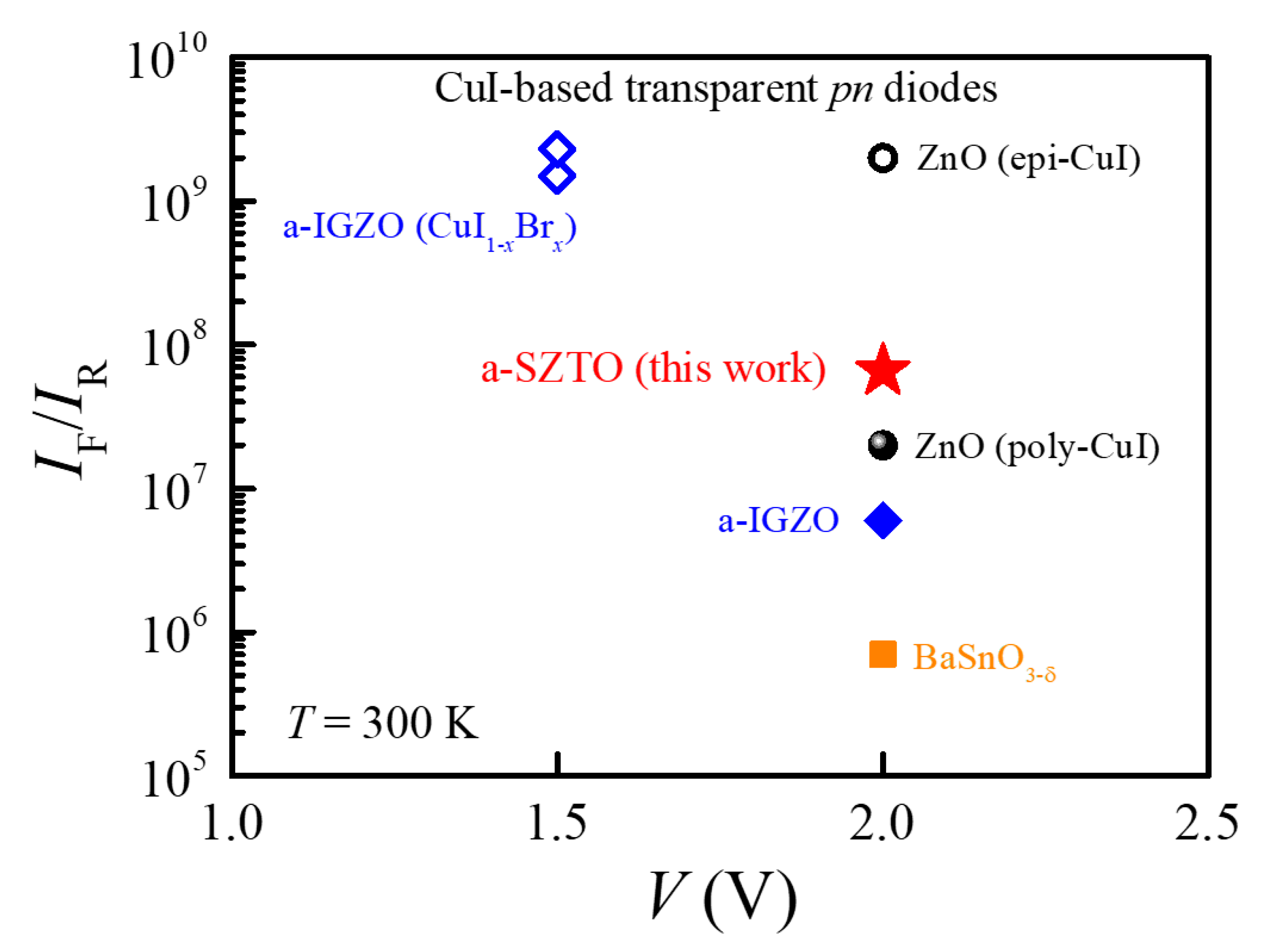
It is emphasized that
IF/
IR = 6.6 × 10
7 is quite a high value among the heterojunction diodes consisting of the
p-CuI film.
Figure 4 compares
IF/
IR of the
p-CuI/
n-SZTO diodes with those of other CuI-based transparent heterojunction diodes that have a high
IF/
IR > ≈10
5; 2 × 10
7 at ±2 V for
p-CuI/
n-ZnO (a polycrystalline CuI film) [
2], 2 × 10
9 at ±2 V for
p-CuI/
n-ZnO (an epitaxial CuI film) [
11], 7 × 10
5 at ±2 V for
p-CuI/
n-BaSnO
3−δ [
12], 6 × 10
6 at ±2 V for
p-CuI/
n-IGZO [
3], and ≈10
9 at ±1.5 V for
p-CuI
1−xBr
x/
n-IGZO (
x = 0.0 − 1.0) [
10]. Albeit the highest value of
IF/
IR = ≈2 × 10
9 realized in the
p-CuI/
n-ZnO diode is higher than that of the present
p-CuI/
n-SZTO diode by ≈30 times, to realize such a diode requires a special growth condition, i.e., an epitaxial growth of the CuI film on top of an epitaxial ZnO film. This implies that such a high
IF/
IR is hard to achieve in a flexible device. Although the
IF/
IR = ≈1 × 10
9 in the
p-CuI/
n-IGZO diodes looks also higher than that of the
p-CuI/
n-SZTO diode, a proper comparison of
IF/
IR might be required as the work used the measured
IF and the fitted
Is [
10].
To quantitatively compare the performance of various diodes made of the
p-type CuI and
n-type materials, several diode parameters and photo-response results are also summarized in
Table 1. The main parameter that characterizes the one-way electrical transport of a diode is
IF/
IR. Most of the diode exhibit
IF/
IR larger than ≈7 × 10
5 except recent two devices with rather large interface areas as they focus on the increase of photocurrent in the
pn diode [
9,
19]. The ideality factor
η seems to be lower than 2 when the
n-type materials are epi-films of ZnO or amorphous IGZO film while the
η of the
p-CuI/
n-SZTO is as large as 2.7–3.0, indicating that disorder effects in the CuI film can be further reduced by better annealing or growth conditions. The
Is of the
p-CuI/
n-SZTO diode is much lower than those of the
p-CuI/
n-ZnO and the
p-CuI
1−xBr
x/
n-IGZO diodes due to the inclusion of offset current in the fitting process. The
Rs value of the
p-CuI/
n-SZTO is still higher than those of other diodes, leaving rooms for improvement by reducing interface resistance at the
pn junction and
p- or
n-type films/electrodes. Therefore, if the
Rs and the
η can be further improved in the
p-CuI/
n-SZTO, the
IF/
IR is likely to be enhanced more. Finally, in
Table 1, to illustrate a direction of future applications, we have also listed several recent cases where the photo responsivity has been tested in the transparent
pn diode made of the
p-CuI. Based on these recent related studies, it is expected that flexible, optically transparent, cheap UV photodetectors can be fabricated by the
p-CuI/
n-SZTO diode.
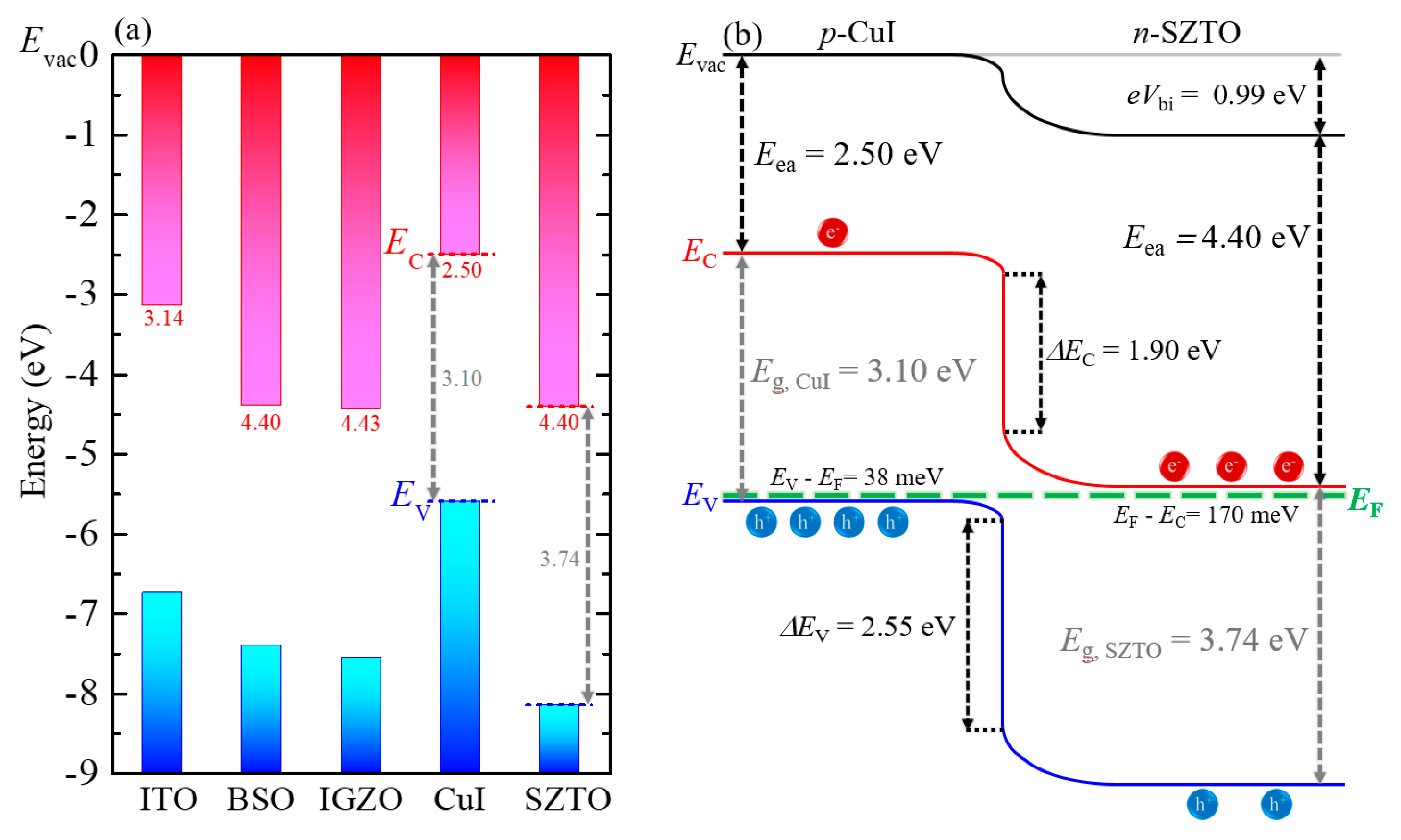
Figure 5a compares the energy band alignment of several wide bandgap materials, including CuI [
2,
12], SZTO [
13,
22], IGZO [
8,
24], BaSnO
3 [
12,
25], and ITO [
26]. Based on the experimental results from previous reports, the band energies of those materials are aligned at the vacuum energy level
Evac = 0. The top (red) and bottom (blue) columns present conduction and valance bands, respectively. In order to investigate the energy band diagram of the annealed CuI (140 nm)/SZTO diode shown in
Figure 5b, first of all, several energies such as
Evac, valance band maximum (
EV), and conduction band minimum (
EC) are determined from
Figure 5a. Subsequently, the Fermi energy level (
EF) is calculated from the Anderson diode model for heterojunction [
27]; various input parameters of valance band maximum
EV, conduction band minimum
EC [
2,
13], dielectric constant [
2,
22], and effective masses [
22,
28] of both CuI and SZTO are adopted from the literature.
Eg and
n of SZTO are estimated from our previous work [
13], while
Eg and
p of CuI are obtained in this work. Basic parameters and related references are summarized in
Table 2.
The resultant band diagram is consistent with the type-II band alignment (or staggered gap type), in which
EC of the
n-type material is located at the energy window between
EC and
EV of the
p-type material. The predicted
eVbi, the depletion width of CuI, and the depletion width of SZTO are found as 0.99 eV, 0.03 nm, and 37.1 nm, respectively. The present CuI/SZTO diode is indeed the one-side abrupt junction, of which the depletion region is mostly formed at, in this case, the SZTO layer. It is noted that the
n-type depletion width of 37.1 nm is larger than the thickness of the SZTO film itself (27 nm). In this condition, an effective negative bias might be formed at the interface, and consequently, a finite forward bias should be required to reduce the electric field and to start the current flow across the
pn diode. Consistent with this scenario, relatively high voltages for the current onset in the |
j|-
V curves have been indeed found at ≈0.7 V in
Figure 2b,d.


