
Combined Structural and Voltage Control of Giant Nonlinearities in Semiconductor Superlattices


1
Department of Physics, Khalifa University of Science and Technology, Abu Dhabi 127788, United Arab Emirates
2
Institute of Physics, Czech Academy of Sciences, 18221 Prague, Czech Republic
*
Author to whom correspondence should be addressed.
Nanomaterials 2021, 11(5), 1287; https://0-doi-org.brum.beds.ac.uk/10.3390/nano11051287
Submission received: 26 March 2021
/
Revised: 3 May 2021
/
Accepted: 11 May 2021
/
Published: 13 May 2021
(This article belongs to the Special Issue Materials for Sources and Detectors in the GIGA-TERA-MIR and NIR-IR Ranges)
Abstract
:Recent studies have predicted a strong increase in high harmonic emission in unbiased semiconductor superlattices due to asymmetric current flow. In parallel, an external static bias has led to orders of magnitude control of high harmonics. Here, we study how this control can affect the operation of superlattice multipliers in a range of input frequencies and powers delivered by commercially available GHz sources. We show that the strongly nonlinear behavior can lead to a very complex scenario. Furthermore, it is natural to ask what happens when we combine both asymmetry and voltage control effects. This question is answered by the simulations presented in this study. The efficiency of high-order even harmonics is increased by the combined effects. Furthermore, the development of ‘petals’ in high-order emission is shown to be more easily achieved, opening the possibility to very interesting fundamental physics studies and more efficient devices for the GHz–THz range.
1. Introduction
Semiconductor superlattices (SSLs) are nanomaterials constructed atom-by-atom by means of epitaxial growth techniques, and they make in many ways, the ideal system to study quantum transport and optics controlling both structural parameters and applied fields [1,2,3]. The experimental detection of coherent Bloch oscillations and Stark ladders [4] was the first step for the development of SSL multipliers (SSLMs) as sources and heterodyne detectors, generating higher order harmonics well within the far-infrared (54th at 37 μm) [5,6]. Compact sources operating at room temperature, such as superlattice electron devices (SLEDs), can deliver so far a 4.2 mW power output at an input frequency of 145 GHz [7]. These SLED structures can in principle be synchronized with the potential to become input sources with a much higher output power [8], which can be combined with SSLMs to create hand-held devices for a large number of state of the art gigahertz–terahertz spectroscopic techniques. This scenario can become even more interesting with quantum dot and graphene superlattices [9,10,11,12,13]. At present, quantum cascade lasers (QCLs) demonstrate high output power in the THz and mid-infrared (MIR) regions [14,15,16], which like the SSLMs are epitaxially grown and multilayered at nanoscale and can also be predictably simulated by a combination of Nonequilibrium Green’s functions, density matrix and Boltzmann equation methods [17,18,19,20,21,22,23,24,25,26,27,28]. QCL emission stems from intersubband optical transitions, in contrast with the mechanisms underlying high-order harmonic generation (HHG) in SSLMs, which we briefly summarize next. When an SSLM is biased, an input oscillating field can modulate the Bloch oscillations giving rise to HHG [29,30,31,32]. This nonlinear emission from the SSLM can be strongly affected by the involvement of electric field domains [33,34]. Strong excitonic effects can also play a role under well-defined conditions [35,36,37]. All these processed can be somehow be combined to enhance HHG in SSLMs; however, in this paper we focus on the combined effect of a uniform bias and current–voltage asymmetry on the Bloch oscillations modulation, which has successfully predicted giant voltage control of HHG in unbiased SSLMs [28,38,39,40,41,42].
2. Materials and Methods
The simulations presented in this paper are based on the optical response of a strongly coupled semiconductor superlattice excited by combined static and oscillating fields. Next we summarize a semiclassical approach, in which the electromagnetic field is treated classically, and the materials by quantum mechanics. The semiclassical approach can be adapted to other nonlinear voltage current cases; however, note that the equations used here are specific for superlattices. The derivation starts from Maxwell’s equations. Assuming linear polarization along , we do not need a vector notation. If there are no bound charges and no magnetization in the medium, we obtain the following wave equation:
where the speed of light is . Simplifying the Boltzmann equation for carrier transport with relaxation approximation, one can show that if the superlattice is illuminated with combined static and monochromatic fields [1,28,38,39,40,41,42],
the nonlinear generation of harmonics and current rectification, with the current I, related to the current density by j = I/A, is described by the following:
The strong nonlinear behavior is dictated mathematically by the Bessel functions of order and first kind, , ruled by , which controls the modulation of Bloch oscillations. In addition, denotes shifted potential drops by an integer number of photon quanta. The charge of an electron, superlattice period and Plank’s constant are given respectively by .
The functions and read as follows:
The global dephasing is given by . It characterizes the region of negative differential resistance and denotes current maximum at . Asymmetric flow in the voltage–current is described by an Ansatz solution introduced in Ref. [28],
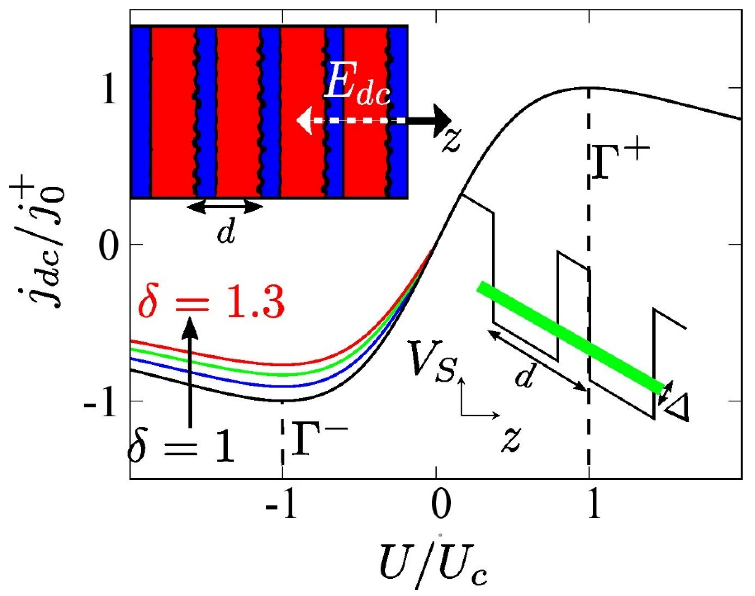
Our calculations are performed for a strongly coupled superlattice consisting of alternating GaAs and AlAs semiconducting layers depicted by red and blue regions, respectively, in the left inset of Figure 1. Therefore, the tight-binding dispersion relation can describe the kinetic energy of the electron in the first SSL miniband, where is the quasimomentum and is the miniband width [1]. Note that typically the interfaces of GaAs over AlAs do not have the same quality as those of AlAs over GaAs. To characterize the quality of interfaces in the superlattice we employ the asymmetry parameter , which effectively depends on the different interface roughness self-energies [39,41]. Therefore, as increases the peak of the current–voltage characteristic for positive bias practically remains the same, whereas for negative bias the peak is significantly reduced. The main input parameters of Equations (3)–(5) taken from Ref. [28] are as follows: , = 21 meV, resulting from Nonequilibrium Green’s functions (NEGF) calculations and nm corresponding to an SSL with 18 lattice periods () of 6.23 nm each, i.e., eighteen monolayers GaAs and four monolayers AlAs homogeneously doped with electron density .
We assume next a slowly varying propagation, so that it is uniform throughout the active region (z-direction). Harmonic electromagnetic fields, current densities and polarizations will build up from zero and we can use a complex representation for plane waves inside a waveguide between x = 0 and x = L. In general,
The equations connecting electric field, vector potential, current and the macroscopic polarization lead to the relations.
where we subsequently insert Equation (7) into (wave) Equation (1).
or equivalently,
thus,
Introducing the complex wavenumber , ,
At this point we introduce a propagation factor The slowly varying amplitude approximation (SVEA), , simplifies the wave equation for the vector potential. Note that we are interested in harmonics.
The harmonic fields and vector potential build up from zero at x = 0, thus,
In semiconductors, the real part of the linear wavenumber is typically much larger than its imaginary part. Thus (for ) we introduce the Ansatz ,
For , we have the following:
The real and imaginary components of are given by , , and typically . Introducing the contact area , the (averaged) power emitted by the order harmonic reads,
where we have approximated the refractive index by the background refractive index . Note that in our calculations we consider a contact area 50 μm2 corresponding to a typical SSL mesa structure with a diameter 8 μm.
3. Results
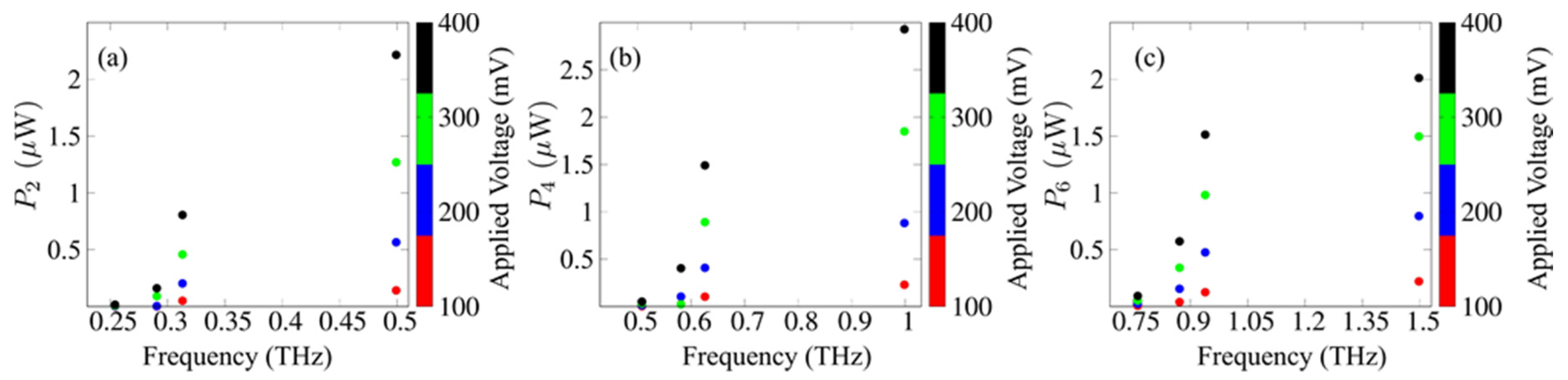
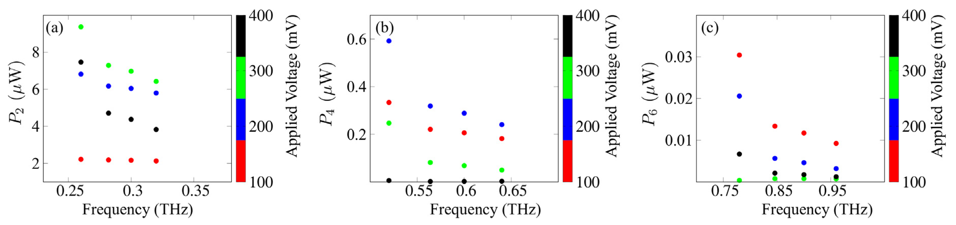
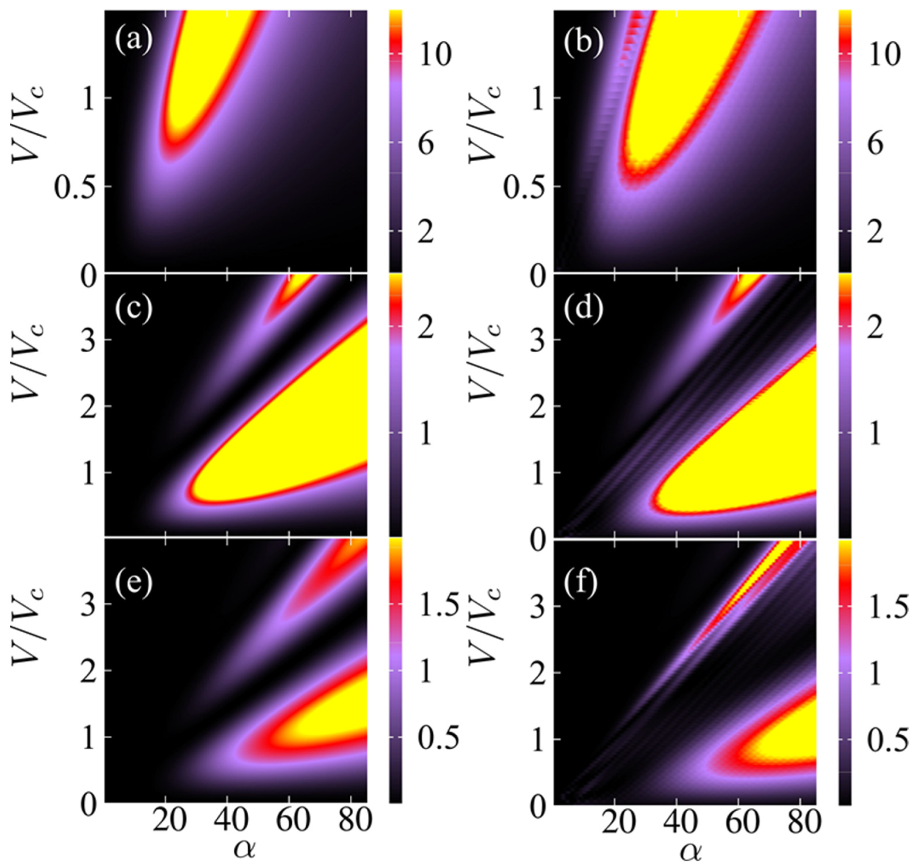
Figure 2 shows the output powers for the second, fourth and sixth harmonics of the SSLMs excited by well-defined SLED input powers and frequencies extracted from experiments [7] that were used for the comparison with different input device powers [4]. Figure 3 shows the corresponding analysis for backward wave oscillators (BWOs) [4,40]. Figure 3 shows the harmonics output power (arb. Units) in a superlattice with period d, as a function of , the applied voltage and the asymmetry parameter . The input parameters are connected by the relation . The black areas designate the set of values (, , δ) for which demonstrates a weak or zero output (see Figure 4a,b). On the other hand, the colored areas reveal discrete ‘islands’ of enhanced harmonic response. Finally, in Figure 5 we fix the level of current asymmetry δ and look at details of the second, fourth and sixth harmonics. In this case, the colored areas indicate ‘petals’ of significant harmonic response as a function only of the voltage, , and the parameter , which is directly proportional to the amplitude of the oscillating field. The high harmonic ‘petals’ are separated by black areas which again are defined by the set of values (, ) for which shows a small harmonic response.
4. Discussion
Figure 2 is based on specific frequencies and input powers delivered by available SLED sources [7,40]. It shows a monotonic increase in the output power with applied voltage. However, the scenario in Figure 3 for powers and frequencies typically delivered by BWOs [28,40] is far more complex. The maximum output for even harmonics occurs in a well-defined region of the input parameters, not necessarily at the largest applied voltage. This is consistent with the predictions and measurements in Ref. [42]. We also expect that current flow asymmetry improves the even harmonics, as predicted in Ref. [41]. Thus, the natural question to ask is, what happens when we combine both, controlling the output with both . Figure 4 and Figure 5 answer this question. We see that the asymmetry allows for strong emission at a lower voltage. This may make the observation of high harmonic ‘petals’ easier, since the available samples, such as those used in the experiments described in Ref. [42], cannot sustain high voltages without permanent sample damage. This can also lead to devices with a more uniform higher power output at high-order even harmonic, leading to a wide range of useful frequencies in the GHz–THz range.
In conclusion, this paper describes the consequence of the combined intrinsic voltage flow asymmetry with an externally applied voltage, predicting an increase in efficiency for even harmonics and the possibility to more easily observe the development of ‘petals’ in high harmonic emission. This unusual nonlinear effect should open new possibilities for applications and fundamental physics studies.
Author Contributions
Conceptualization, methodology, preparation, review and editing, supervision, project administration, funding acquisition: M.F.P.; formal analysis, writing—original draft, simulations and graphics: M.F.P. and A.A. All authors have read and agreed to the published version of the manuscript.
Funding
This publication is based upon work supported by the EU H2020-Europe’s resilience to crises and disasters program (H2020-grant agreement no. 832876, aqua3S)) and by the Czech Science Foundation (GAČR) through grant no. 19-03765S.
Data Availability Statement
The data presented in this study are available on request from the corresponding author.
Conflicts of Interest
The authors declare no conflict of interest.
References
- Wacker, A. Semiconductor superlattices: A model system for nonlinear transport. Phys. Rep. 2002, 357, 1–111. [Google Scholar] [CrossRef] [Green Version]
- Alfadhli, S.A.; Savel’ev, S.E.; Kusmartsev, F.V. Dirac-Weyl points’ manipulation using linear polarized laser field in Floquet crystals for various Graphene superlattices. J. Phys. Conf. Ser. 2018, 961, 012012. [Google Scholar] [CrossRef]
- Pereira, M. Analytical Expressions for Numerical Characterization of Semiconductors per Comparison with Luminescence. Materials 2018, 11, 2. [Google Scholar] [CrossRef] [Green Version]
- Waschke, C.; Roskos, H.G.; Schwedler, R.; Leo, K.; Kurz, H.; Köhler, K. Coherent Submillimeter-Wave Emission from Bloch Oscillations in a Semiconductor Superlattice. Phys. Rev. Lett. 1993, 70, 3319–3322. [Google Scholar] [CrossRef] [PubMed]
- Vaks, V. High-Precise Spectrometry of the Terahertz Frequency Range: The Methods, Approaches and Applications. J. Infrared Milli. Terahz. Waves 2012, 33, 43–53. [Google Scholar] [CrossRef]
- Pavelyev, D.G.; Skryl, A.S.; Bakunov, M.I. High-resolution broadband terahertz spectroscopy via electronic heterodyne detection of photonically generated terahertz frequency comb. Opt. Lett. 2014, 39, 5669–5672. [Google Scholar] [CrossRef] [PubMed]
- Eisele, H.; Li, L.; Linfield, E.H. High-performance GaAs/AlAs superlattice electronic devices in oscillators at frequencies 100–320 GHz. Appl. Phys. Lett. 2018, 112, 172103. [Google Scholar] [CrossRef] [Green Version]
- Gaifullin, M.B.; Alexeeva, N.V.; Hramov, A.E.; Makarov, V.V.; Maksimenko, V.A.; Koronovskii, A.A.; Greenaway, M.T.; Fromhold, T.M.; Patané, A.; Mellor, C.J.; et al. Balanov, Microwave Generation in Synchronized Semiconductor Superlattices. Phys. Rev. Appl. 2017, 7, 044024. [Google Scholar] [CrossRef] [Green Version]
- Dhillon, S.S.; Vitiello, M.S.; Linfield, E.H.; Davies, A.G.; Hoffmann, M.C.; Booske, J.; Paoloni, C.; Gensch, M.; Weightman, P.; Williams, G.P.; et al. The 2017 terahertz science and technology roadmap. J. Phys. D Appl. Phys. 2017, 50, 043001. [Google Scholar] [CrossRef]
- Mittelstädt, A.; Greif, L.A.T.; Jagsch, S.T.; Schliwa, A. Terahertz lasing at room temperature: A numerical study of a vertical-emitting quantum cascade laser based on a quantum dot superlattice. Phys. Rev. B 2021, 103, 115301. [Google Scholar] [CrossRef]
- Ferrari, A.C. Science and technology roadmap for graphene, related two-dimensional crystals, and hybrid systems. Nanoscale 2015, 7, 4598–4810. [Google Scholar] [CrossRef] [Green Version]
- Pereira, M.F.; Shulika, O. Terahertz and Mid Infrared Radiation: Detection of Explosives and CBRN (Using Terahertz). In NATO Science for Peace and Security Series B: Physics and Biophysics; Springer: Dordrecht, The Netherlands, 2014; ISBN 978-94-017-8571-6. [Google Scholar]
- Pereira, M.F.; Shulika, O. Terahertz and Mid Infrared Radiation: Generation, Detection and Applications. In NATO Science for Peace and Security Series B: Physics and Biophysics; Springer Science & Business Media B.V.: Berlin, Germany, 2011; ISBN 978-94-007-0768-9. [Google Scholar]
- Faist, J.; Capasso, F.; Sivco, D.L.; Sirtori, C.; Hutchinson, A.L.; Cho, A.Y. Quantum Cascade Laser. Science 1994, 264, 553–556. [Google Scholar] [CrossRef]
- Köhler, R.; Tredicucci, A.; Beltram, F.; Beere, H.E.; Linfield, E.H.; Davies, A.G.; Ritchie, D.A.; Iotti, R.C.; Rossi, F. Terahertz semiconductor-heterostructure laser. Nature 2002, 417, 156–159. [Google Scholar] [CrossRef]
- Razeghi, M.; Lu, Q.Y.; Bandyopadhyay, N.; Zhou, W.; Heydari, D.; Bai, Y.; Slivken, S. Quantum cascade lasers: From tool to product. Opt. Express 2015, 23, 8462–8475. [Google Scholar] [CrossRef]
- Schmielau, T.; Pereira, M.F. Nonequilibrium many body theory for quantum transport in terahertz quantum cascade lasers. Appl. Phys. Lett. 2009, 95, 231111. [Google Scholar] [CrossRef]
- Pereira, M.F.; Lee, S.-C.; Wacker, A. Controlling many-body effects in the midinfrared gain and terahertz absorption of quantum cascade laser structures. Phys. Rev. B 2004, 69, 205310. [Google Scholar] [CrossRef] [Green Version]
- Pereira, M.F.; Wenzel, H. Interplay of Coulomb and nonparabolicity effects in the intersubband absorption of electrons and holes in quantum wells. Phys. Rev. B 2004, 70, 205331. [Google Scholar] [CrossRef]
- Pereira, M.F. Intervalence transverse-electric mode terahertz lasing without population inversion. Phys. Rev. B 2008, 78, 245305. [Google Scholar] [CrossRef]
- Pereira, M.F.; Tomić, S. Intersubband gain without global inversion through dilute nitride band engineering. Appl. Phys. Lett. 2011, 98, 061101. [Google Scholar] [CrossRef] [Green Version]
- Pereira, M.F. The Linewidth Enhancement Factor of Intersubband Lasers: From a Two-Level Limit to Gain without Inversion Conditions. Appl. Phys. Lett. 2016, 109, 222102. [Google Scholar] [CrossRef] [Green Version]
- Winge, D.O.; Franckie, M.; Verdozzi, C.; Wacker, A.; Pereira, M.F. Simple electron-electron scattering in non-equilibrium Green’s function simulations. J. Phys. Conf. Ser. 2016, 696, 012013. [Google Scholar] [CrossRef] [Green Version]
- Wacker, A.; Lindskog, M.; Winge, D.O. Nonequilibrium Green’s Function Model for Simulation of Quantum Cascade Laser Devices Under Operating Conditions. IEEE J. Sel. Top. Quantum Electron. 2013, 19, 1200611. [Google Scholar] [CrossRef]
- Franckié, M.; Faist, J. Bayesian optimization of terahertz quantum cascade lasers. Phys. Rev. Appl. 2020, 13, 034025. [Google Scholar] [CrossRef] [Green Version]
- Gajić, A.; Radovanović, J.; Vuković, N.; Milanović, V.; Boiko, D.L. Theoretical approach to quantum cascade micro-laser broadband multimode emission in strong magnetic fields. Phys. Lett. A 2021, 387, 127007. [Google Scholar] [CrossRef]
- Vukovic, N.; Radovanovic, J.; Milanovic, V.; Boiko, D.L. Numerical study of Risken–Nummedal–Graham–Haken instability in mid-infrared Fabry–Pérot quantum cascade lasers. Opt. Quantum Electron. 2020, 52, 91. [Google Scholar] [CrossRef]
- Pereira, M.F.; Winge, D.; Wacker, A.; Zubelli, J.P.; Rodrigues, A.S.; Anfertev, V.; Vaks, V. Theory and Measurements of Harmonic Generation in Semiconductor Superlattices with Applications in the 100 GHz to 1 THz Range. Phys. Rev. B 2017, 96, 045306. [Google Scholar] [CrossRef] [Green Version]
- Winnerl, S.; Schomburg, E.; Brandl, S.; Kus, O.; Renk, K.F.; Wanke, M.C.; Allen, S.J.; Ignatov, A.A.; Ustinov, V.; Zhukov, A.; et al. Frequency doubling and tripling of terahertz radiation in a GaAs/AlAs superlattice due to frequency modulation of bloch oscillations. Appl. Phys. Lett. 2000, 77, 1259. [Google Scholar] [CrossRef]
- Schomburg, E.; Grenzer, J.; Hofbeck, K.; Dummer, C.; Winnerl, S.; Ignatov, A.; Renk, K.; Pavel’Ev, D.; Koschurinov, J.; Melzer, B.; et al. Superlattice frequency multiplier for generation of submillimeter waves. IEEE J. Sel. Top. Quantum Electron. 1996, 2, 724. [Google Scholar] [CrossRef]
- Ignatov, A.A.; Schomburg, E.; Grenzer, J.; Renk, K.F.; Dodin, E.P. THz-field induced nonlinear transport and dc voltage generation in a semiconductor superlattice due to bloch oscillations. Z. Phys. 1995, 98, 187–195. [Google Scholar] [CrossRef]
- Romanov, Y.A.; Romanova, Y.Y. Bloch oscillations in superlattices: The problem of a terahertz oscillator. Semiconductors 2005, 39, 147. [Google Scholar] [CrossRef]
- Le Person, H.; Minot, C.; Boni, L.; Palmier, J.F.; Mollot, F. Gunn oscillations up to 20 GHz optically induced in GaAs/AlAs superlattice. Appl. Phys. Lett. 1992, 60, 2397. [Google Scholar] [CrossRef]
- Schomburg, E. Current oscillation in superlattices with different miniband widths. Phys. Rev. B 1998, 58, 4035. [Google Scholar] [CrossRef]
- Meier, T.; Von Plessen, G.; Thomas, P.; Koch, S.W. Coherent electric-field effects in semiconductors. Phys. Rev. Lett. 1994, 73, 902. [Google Scholar] [CrossRef]
- Dignam, M. Excitonic bloch oscillations in a terahertz field. Phys. Rev. B 1999, 59, 5770. [Google Scholar] [CrossRef]
- Wang, D.; Zhang, A.; Yang, L.; Dignam, M.M. Tunable terahertz amplification in optically excited biased semiconductor superlattices: Influence of excited excitonic states. Phys. Rev. B 2008, 77, 115307. [Google Scholar] [CrossRef]
- Pereira, M.F.; Anfertev, V.; Zubelli, J.P.; Vaks, V. THz Generation by GHz Multiplication in Superlattices. J. Nanophotonics 2017, 11, 046022. [Google Scholar] [CrossRef]
- Apostolakis, A.; Pereira, M.F. Controlling the harmonic conversion efficiency in semiconductor superlattices by interface roughness design. AIP Adv. 2019, 9, 015022. [Google Scholar] [CrossRef] [Green Version]
- Apostolakis, A.; Pereira, M.F. Potential and limits of superlattice multipliers coupled to different input power sources. J. Nanophotonics 2019, 13, 036017. [Google Scholar] [CrossRef]
- Apostolakis, A.; Pereira, M.F. Superlattice nonlinearities for Gigahertz-Terahertz generation in harmonic multipliers. Nanophotonics 2020, 9, 3941–3952. [Google Scholar] [CrossRef]
- Pereira, M.F.; Anfertev, V.; Shevchenko, Y.; Vaks, V. Giant controllable gigahertz to terahertz nonlinearities in superlattices. Sci. Rep. 2020, 10, 15950. [Google Scholar] [CrossRef]
Figure 1.
The current–voltage characteristics, in the absence of an oscillating field for different values of the asymmetry parameter, from bottom (black) to top (red) as follows: . The left inset is a schematic representation of the semiconductor superlattice with a superlattice period, d, which results in the asymmetric current flow. The SSL is biased by a static electric field antiparallel to the growth axis (−z) of the superlattice structure. The right inset corresponds to the tilted superlattice potential due to the application of the electric field. The shaded green region indicates the first miniband with width .

Figure 2.
(a) Second, (b) fourth and (c) sixth harmonics output powers for SSL multipliers under the influence of a biased oscillating field for different input SLED devices over frequency ranges 250–1500 GHz for a perfectly symmetric current–voltage curve. The input frequencies and powers given respectively by 127.1, 145.3, 156.5, 249.6 GHz and 14, 4.2, 1.7, 0.92 mW.

Figure 3.
(a) Second, (b) fourth and (c) sixth harmonics output powers for SSL multipliers under the influence of a biased oscillating field for different input BWO devices over frequency ranges 250–950 GHz for a perfectly symmetric current–voltage curve. The input frequencies and powers given respectively by 130, 141, 150, 160 GHz and 61.6, 47, 45.2, 42.2 μW.

Figure 4.
(a) Third harmonic (a) second and (b) third harmonics output powers (arb. units) in a superlattice with period , as a function of , V (voltage) and δ (asymmetry parameter). This parameter is directly proportional to the input electromagnetic field oscillating at ν = 249 GHz. The control voltage, is given as a ratio with respect to the critical voltage , which characterizes negative differential resistance . The idea is to focus on the voltage, field and asymmetry control.

Figure 5.
(a,b) Second, (c,d) fourth and (e,f) sixth harmonics output powers (arb. units) in a superlattice with period d, for δ = 1 (a,c,e) and δ = 1.3 (b,d,f), as a function of , V (voltage) and δ (asymmetry parameter). The input electromagnetic field oscillates at ν = 249 GHz. The control voltage, is given as a ratio with respect to the critical voltage , which characterizes negative differential resistance.

Publisher’s Note: MDPI stays neutral with regard to jurisdictional claims in published maps and institutional affiliations. |
© 2021 by the authors. Licensee MDPI, Basel, Switzerland. This article is an open access article distributed under the terms and conditions of the Creative Commons Attribution (CC BY) license (https://creativecommons.org/licenses/by/4.0/).
Share and Cite
MDPI and ACS Style
Pereira, M.F.; Apostolakis, A. Combined Structural and Voltage Control of Giant Nonlinearities in Semiconductor Superlattices. Nanomaterials 2021, 11, 1287. https://0-doi-org.brum.beds.ac.uk/10.3390/nano11051287
AMA Style
Pereira MF, Apostolakis A. Combined Structural and Voltage Control of Giant Nonlinearities in Semiconductor Superlattices. Nanomaterials. 2021; 11(5):1287. https://0-doi-org.brum.beds.ac.uk/10.3390/nano11051287
Chicago/Turabian StylePereira, Mauro Fernandes, and Apostolos Apostolakis. 2021. "Combined Structural and Voltage Control of Giant Nonlinearities in Semiconductor Superlattices" Nanomaterials 11, no. 5: 1287. https://0-doi-org.brum.beds.ac.uk/10.3390/nano11051287
Note that from the first issue of 2016, this journal uses article numbers instead of page numbers. See further details here.