1. Introduction
In an effort to reduce the power consumption of battery-powered devices, analog signal processing is being reinvestigated to supplement and/or replace digital systems for making early decisions regarding incoming sensor information. However, analog systems are extremely sensitive to biasing conditions and, thus, need accurate control over their parameters to achieve the desired performance. Particularly in systems consisting of arrays of analog elements, such as field-programmable analog arrays [
1,
2,
3] and other programmable analog arrays [
4,
5,
6], a large number of analog parameters must be precisely established to achieve the desired performance.
Floating-gate (FG) transistors can serve as key enabling devices for such low-power analog systems. An FG transistor is a MOSFET that has no resistive connection to its gate; instead, a “control gate” couples capacitively onto the transistor’s “floating gate.” As a result, the charge on the FG is held fixed under nominal conditions but can be modified via Fowler-Nordheim tunneling and hot-electron injection, which both require elevated voltages. Because of its nonvolatile memory characteristics, FG transistors are ubiquitous in digital systems in the form of EEPROM and Flash memory. However, the ability to finely tune the amount of programmed charge on the FG allows these devices to be used as nonvolatile
analog memory elements, as well. Consequently, FG transistors have found applications as variable threshold-voltage devices, programmable voltage/current sources, analog trimming for device matching, and within adaptive/learning circuits [
7].
Modifying the stored charge on an FG transistor, which is often referred to as “programming” the FG, requires large voltages (typically 2–3 times greater than the rated
of the process) to be applied to the FG transistor terminals in a controlled manner.
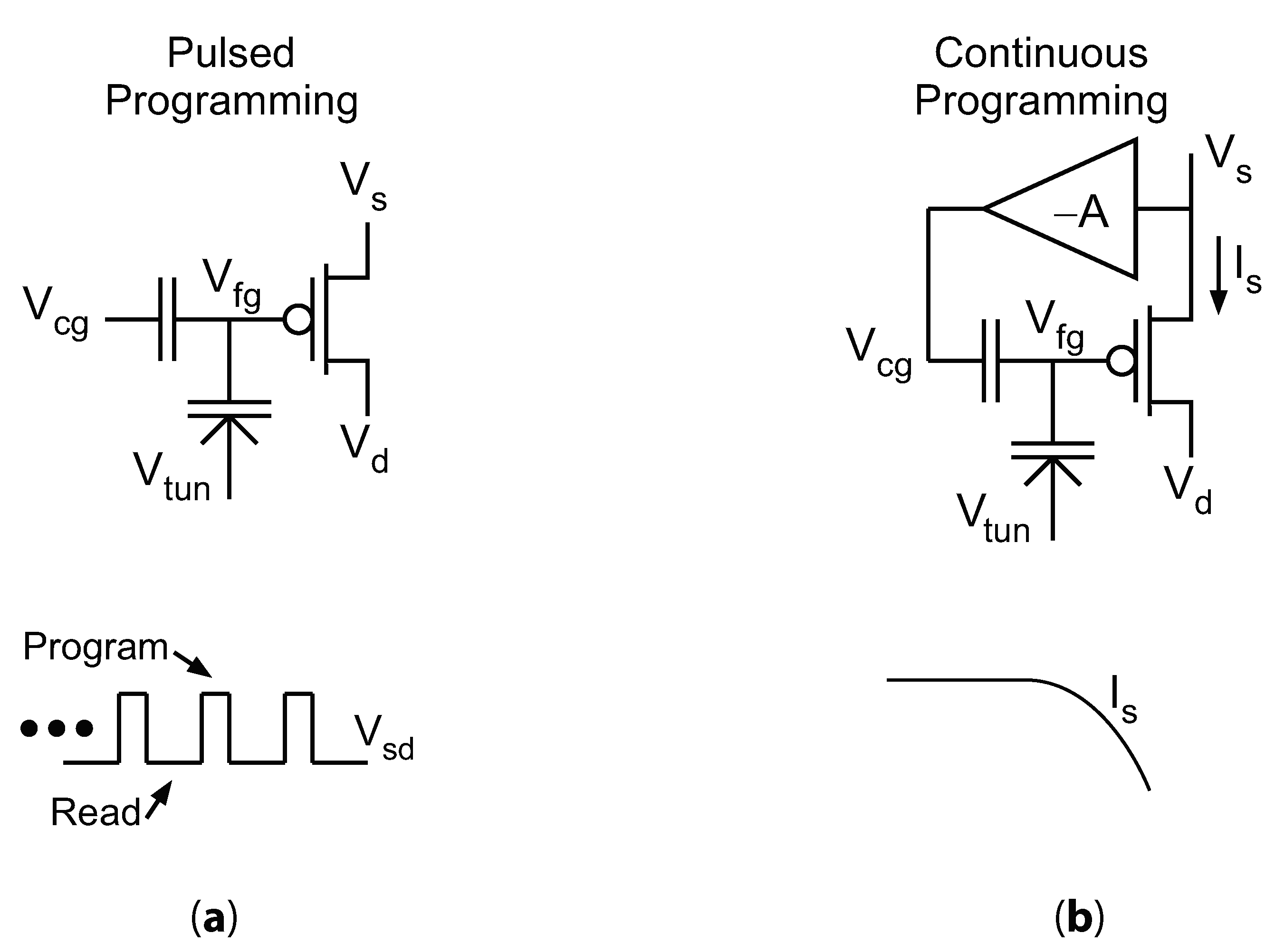
Figure 1 depicts the two primary methods for programming an FG transistor—pulsed and continuous methods. Pulsed methods operate by iteratively applying short, high-voltage pulses to modify the charge and then measuring the FG after each pulse, repeating until a desired target is reached. Continuous methods, on the other hand, apply a constant high voltage and leverage feedback to ensure that the FG charge converges to the desired value. Pulse-based methods have dominated analog applications (e.g., [
8]) because of the simplicity of design and high accuracy that has been demonstrated. However, continuous programming promises to be faster and require less peripheral circuitry than pulse-based programming, which are critical features in resource-constrained systems that need to save power and area.
In this paper, we describe a compact FG cell for continuous programming, which when combined with our simple programmer circuit, converges to target voltages with 13.0 bit resolution. This FG cell/programmer combination is primarily designed to work with battery-powered applications. This work is an extension of our early results in [
9] in which the circuit was constructed using custom discrete elements and achieved far lower accuracy. Here, we present a fully integrated solution with far better programming accuracy and resolution. We also extend the results of a single memory cell in [
9] to array applications. We describe how to build and program FG arrays in a serial (i.e., one at a time) fashion as well as present a method for parallelizing the programming of FG cells in an FG memory array to improve overall programming speed (first described in Masters Thesis [
10]). This paper serves to provide a description on how to build easy-to-use programmable arrays of analog non-volatile memory for low-power applications.
Our basic memory cell uses an FG transistor in a source-follower configuration and linearizes injection via negative feedback to the control gate, as shown in
Figure 1b. Such linear source-feedback injection has been used previously in [
11], but we accomplish the same characteristics with the smaller current conveyor circuit. In addition to being smaller, this current conveyor memory cell also offers more flexible control over the injection rate since the FG source voltage,
, can be modified using either a voltage or a current input.
We describe the development of this system in the remainder of this paper.
Section 2 provides an overview of FG programming.
Section 3 describes various methods of continuous-time FG programming.
Section 4 discusses our current-conveyor-based memory cell.
Section 5 then describes the programmer circuit that is used to achieve specific target values.
Section 6 discusses the two major methodologies to program an FG array—serial and parallel programming.
Section 7 demonstrates the use of an FG array to precisely establish the corner frequencies of a programmable bandpass filter bank. Finally,
Section 8 provides concluding remarks.
2. Overview of Floating-Gate Programming
Two phenomena are typically used to program FG transistors: hot-electron injection and Fowler-Nordheim tunneling. Injection occurs when a large source-to-drain potential (typically
) is applied to a PMOS FG transistor, thus causing high-energy carriers to impact-ionize at the drain. A fraction of the resulting ionized electrons disperse toward the surface with enough energy to overcome the oxide barrier and inject onto the FG. In the subthreshold region, which is our target operational region for low-power applications and high injection efficiency, the injection current from
to
can be approximated as
where
,
, and
are device-dependent fits [
12]. Tunneling, on the other hand, requires high voltages (typically
). To avoid write disturbs during tunneling, unselected array elements must either be disconnected from the tunneling voltage using high-voltage switches or the FGs of the unselected elements must be raised to a sufficient voltage that tunneling does not occur. Due to this difficulty in isolating tunneling within an array, tunneling is typically used only for global erasure in analog memory arrays, while injection is used to write to individual elements. Consequently, we focus mainly on injection in this paper.
Due to their ability to provide dense, low-power, analog biases, FGs are elemental in large-scale programmable analog systems—such as filter banks [
4], classifiers [
5], and field-programmable analog arrays [
1,
13]. In these systems, circuit parameters (e.g., corner frequencies) are controlled by the charge on the FGs; as a result, system performance depends strongly on the programming accuracy. Prior pulse-based programming techniques have achieved high accuracy [
8,
11]. One advantage that pulse-based techniques have in terms of accuracy is that the FG is measured in a state that is similar to run-mode: with no high programming voltages applied to the cell, and with the same current levels that will be used in run-mode. Unfortunately, pulsing is inherently slow due to the time spent reading, during which the high programming voltages are stepped down and the FG is allowed to settle before the measurement is taken; if measuring low currents, which is necessary in low-power applications, then the read time further increases due to the long integration time that is necessary for accurate measurement. Methods to increase the programming speed with pulse-based programming rely on precise knowledge of each FG’s characteristics, so that each pulse can move more aggressively toward the target [
8], but this adds to the complexity. Additionally, pulsing techniques require high-precision data conversion and pulse timing, and possibly large-range current measurement [
14], all of which complicate the inclusion of analog FG memory in simple, resource-constrained systems. Thus, there is a need for fast, compact, low-overhead, and accurate programming: we posit that continuous-time programming is more appropriate for resource-constrained systems.
3. Continuous-Time Floating Gate Programming
Continuous-time FG programming is accomplished by using feedback to stop programming when the memory cell reaches its target value. A variety of continuous programming circuits have been presented, ranging from a single-transistor circuit [
12] that self-converges due to the negative feedback of injection current from the FG to the drain, to more complex circuits with improved speed and accuracy.
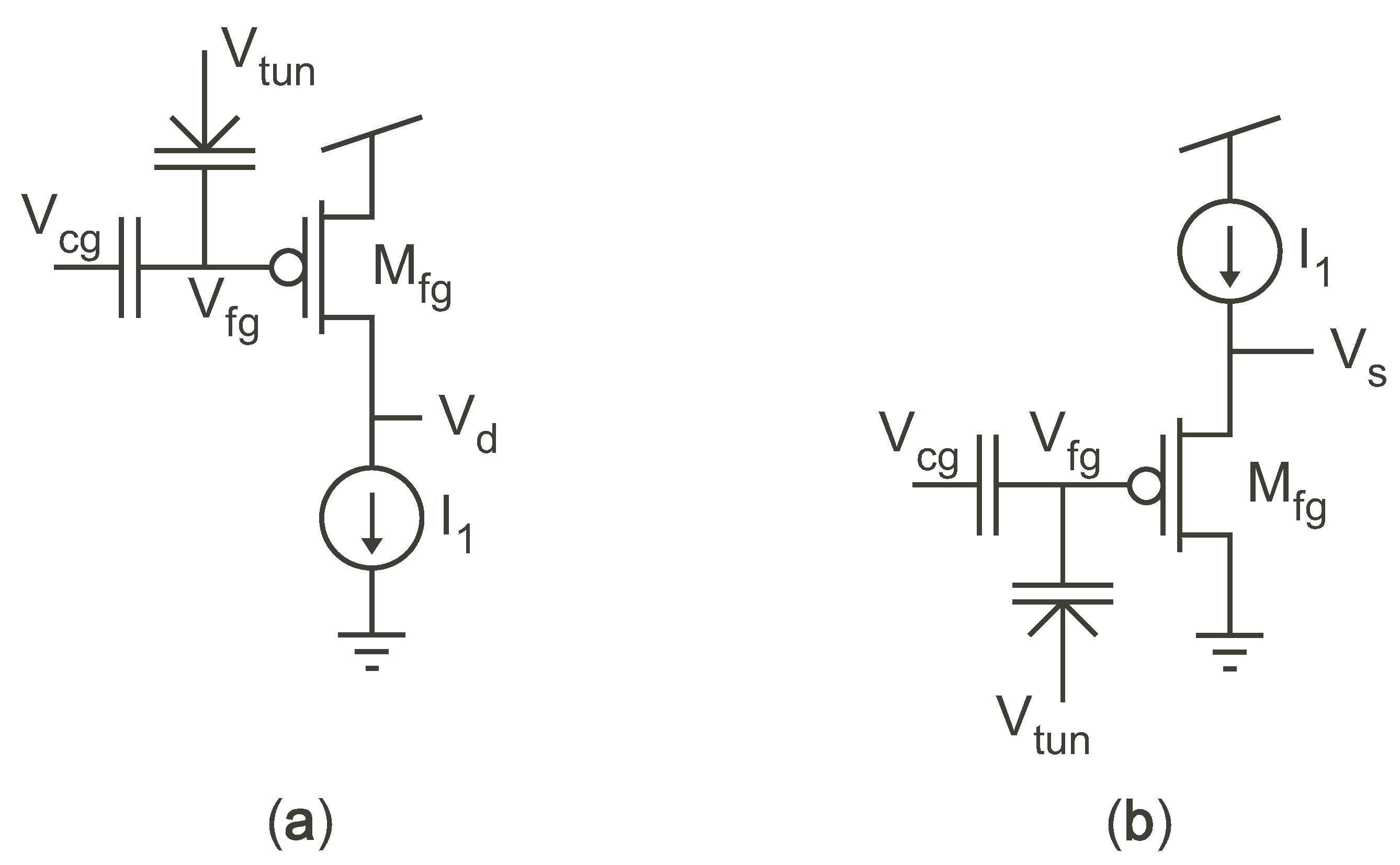
Figure 2 shows the two primary types of FG cells for self-converging, continuous programming that use the inherent feedback in MOSFETs undergoing hot-electron injection to converge to a final value. For both the circuits, as electrons are injected onto the FG, the FG voltage,
, decreases. As a result, the source-to-drain potential also decreases, and, according to Equation (
1), the injection current decreases and will eventually shut off. The circuit in
Figure 2a, which was presented in [
12], provides repeatable results and can be programmed to different targets either by using different values of
for a constant
, or by using different values of
for a constant
. However, the convergence time depends on the initial conditions; if the initial charge on the FG is too high, then the device cannot initially produce
. As a result, injection starts very slowly, and the total time to converge can be long (even though the final stages of convergence occur quickly). While the circuit of
Figure 2b will typically start injecting quickly, it will slowly converge to its final value, often on the order of minutes to converge. Whereas the circuit of
Figure 2a starts slow and finishes quickly, the circuit of
Figure 2b starts quickly and finishes slowly. Both circuits suffer from potential long convergence times because they only rely on internal feedback to converge.
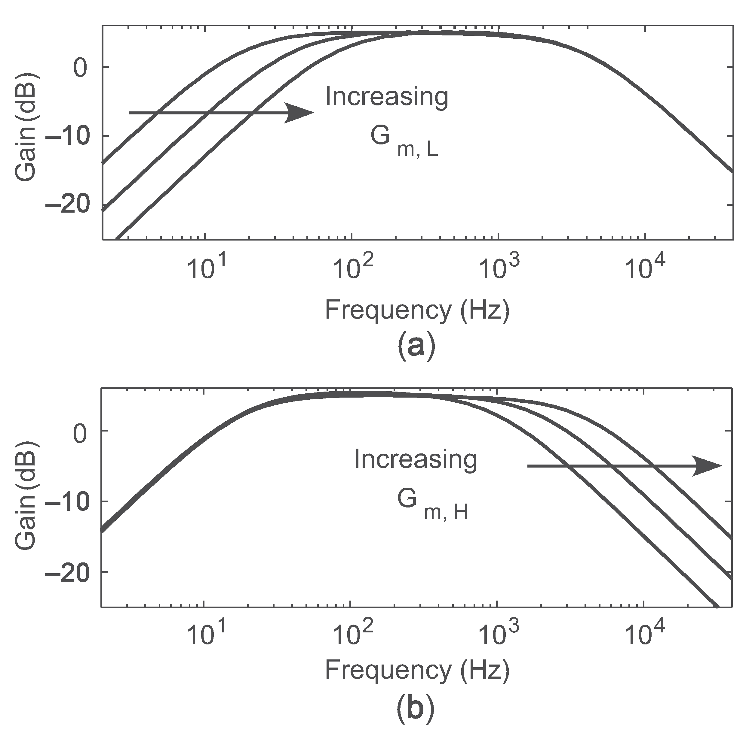
External feedback, on the other hand, can be used to linearize the injection and tunneling processes to ensure that the FG charge is programmed to the desired value in a reasonable and predictable amount of time. External feedback can be used to keep the drain, source, and floating-gate potentials at constant values during the programming process so that injection and/or tunneling occur at a constant rate. As a result, the external feedback can prevent the FG cell from entering a region in which its conditions are not amenable to programming, which would lengthen the programming duration. However, linearizing the programming process means that the FG cell no longer self converges. Instead, systems that linearize the programming rates require additional external circuitry to stop the injection and/or tunneling at the appropriate time.
Several previous circuits were presented that use feedback to linearize the programming process, including memory cells that use a comparator to terminate programming when a target has been reached [
15,
16], memory cells that use differential amplifiers to linearize programming [
17], and a system that uses both hot-electron and hot-hole injection to bidirectionally converge on a target [
18]. In each of these systems, the programming rate is held constant until the target value is reached, and then the programming is abruptly stopped. Such programming faces a severe tradeoff between programming speed and accuracy [
16]. In contrast, the programming circuitry that we present in this work adjusts the FG transistor’s channel current in order to reduce the programming rate as the target value is approached; this adaptation of the current in the FG transistor allows our programmer and FG memory cell to achieve a better tradeoff between programming speed and accuracy.
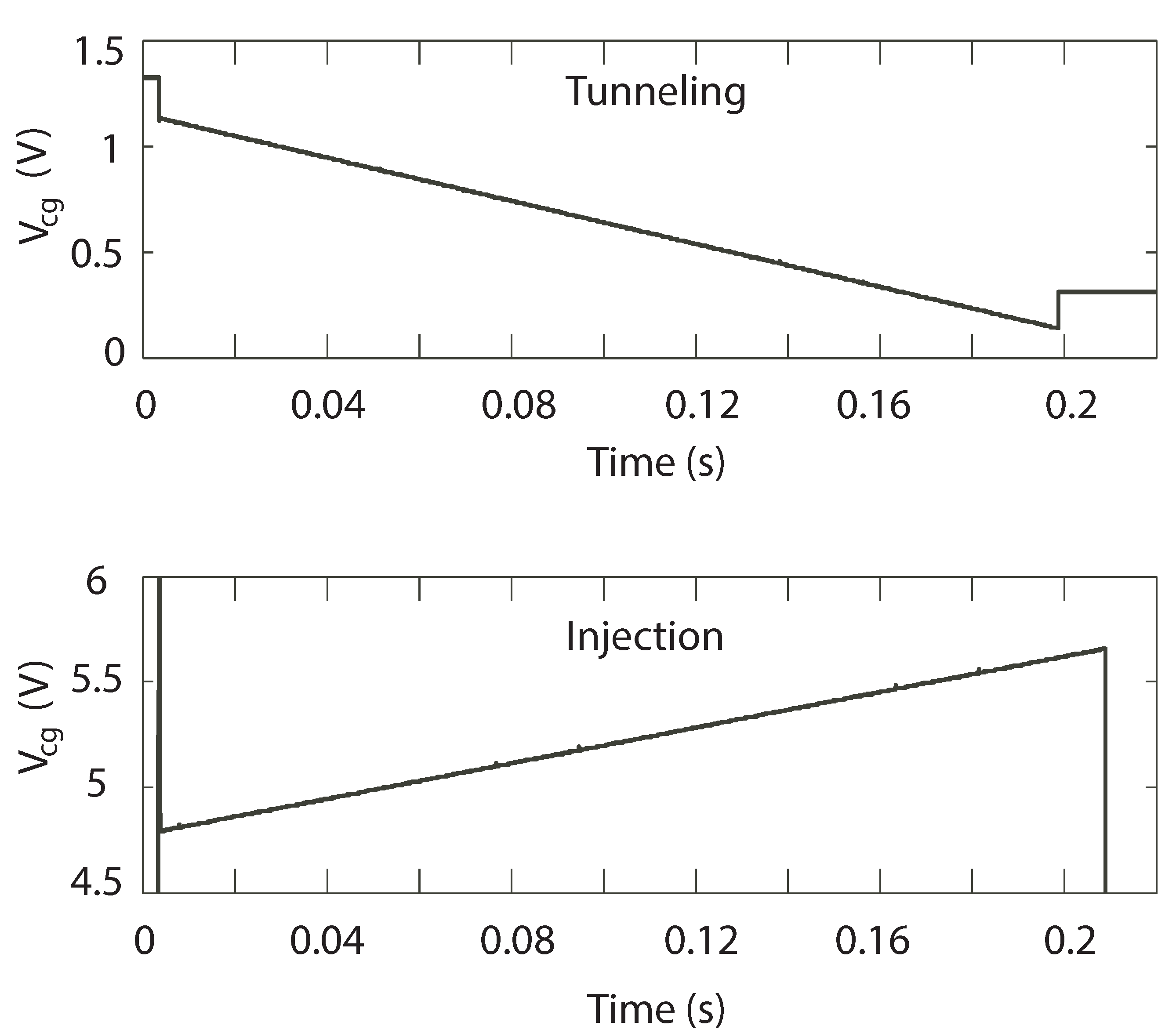
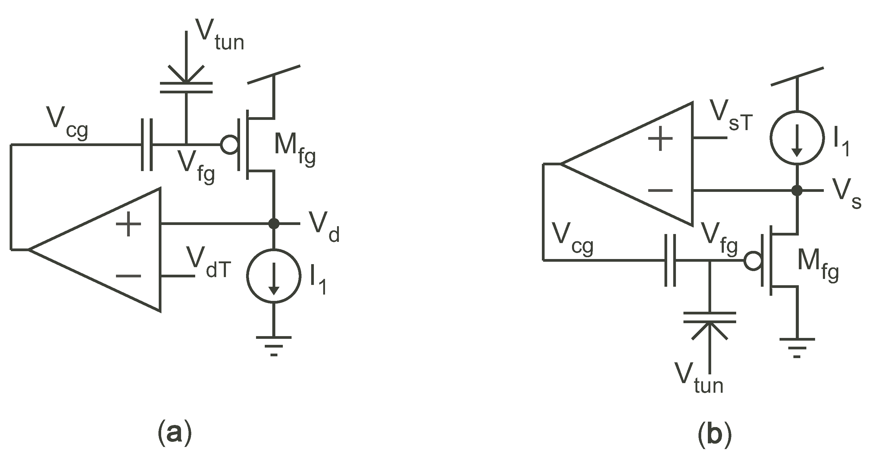
Figure 3 depicts the two primary concepts behind using negative feedback to
to keep all the terminals of
constant through the programming process, and thus keep injection and/or tunneling rates constant. However, as previously mentioned, these memory cells no longer converge on their own, but require additional programming circuitry. In both of these circuits,
is constant and
ramps linearly up during injection, or down during tunneling, to compensate for the change in charge on the FG—see
Figure 4.
thus provides our measure of the charge on the FG. We found the high gain around the loop of the circuit in
Figure 3a to cause stability problems, and so we will not consider it any further. The source follower circuit in
Figure 3b is the same configuration that has been used in pulse-based source-feedback injection to achieve 13-bit precision with program times on the order of 50 s/200 mV [
11]. This circuit has good stability and offers good control over injection and tunneling through the manipulation of both
(which sets
) and
. Our memory cell has the same basic characteristics as this circuit, but is smaller, which is important for large array applications.
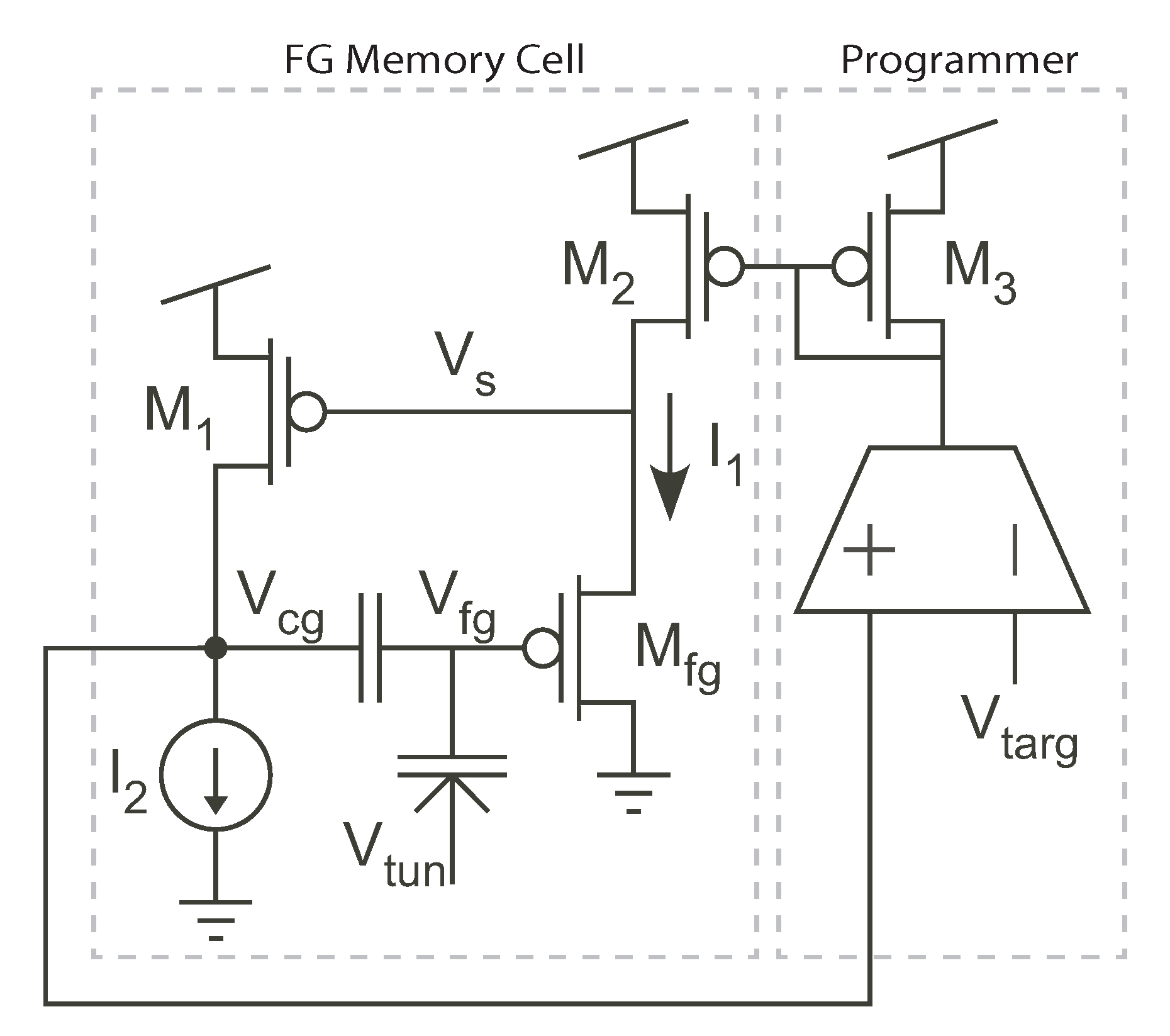
4. Current-Conveyor-Based Memory Cell
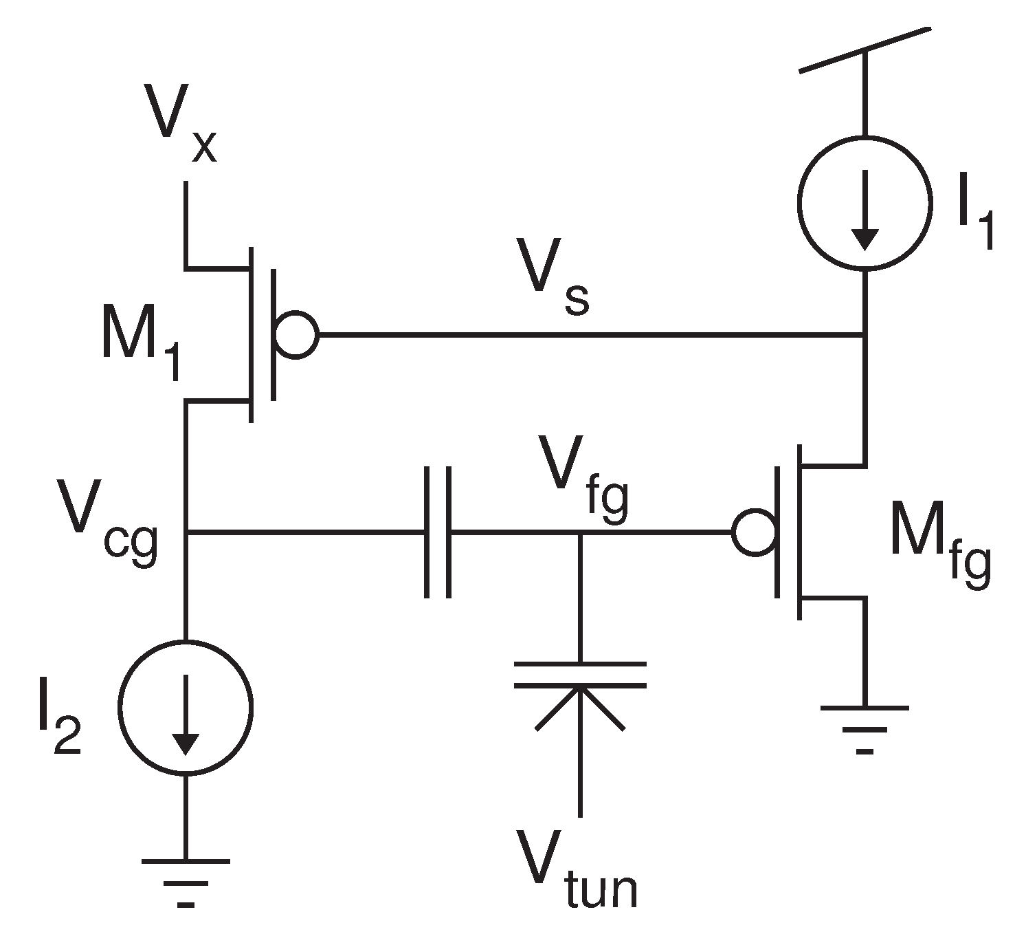
To achieve the good characteristics of the circuit of
Figure 3b but reduce the size, we developed the circuit in
Figure 5. For simplicity, current sources are shown for
and
, but in the actual implementation, each current source is implemented by a single transistor. In this memory cell, the inverting amplifier
–
replaces the op-amp in
Figure 3b. The resulting circuit structure is the current-controlled current conveyor, the details of which can be found in [
19]. In this circuit, the negative feedback adjusts
in order to force both
and
to fixed voltages. The equilibrium point for
is controlled by both the voltage
and the current
. The equilibrium point of
depends on both
and
. Thus, we maintain independent control of the source current and drain-to-source potential (the two main injection parameters) with this four-transistor circuit.
This memory cell offers three control terminals for modifying injection: two currents (
and
) and one voltage (
). Using the subthreshold injection approximation in Equation (
1), we can solve for the injection current as a function of the control terminals in subthreshold operation as
where
is the pre-exponential current scaler for
,
is related to the subthreshold slope for
, and
is the thermal voltage.
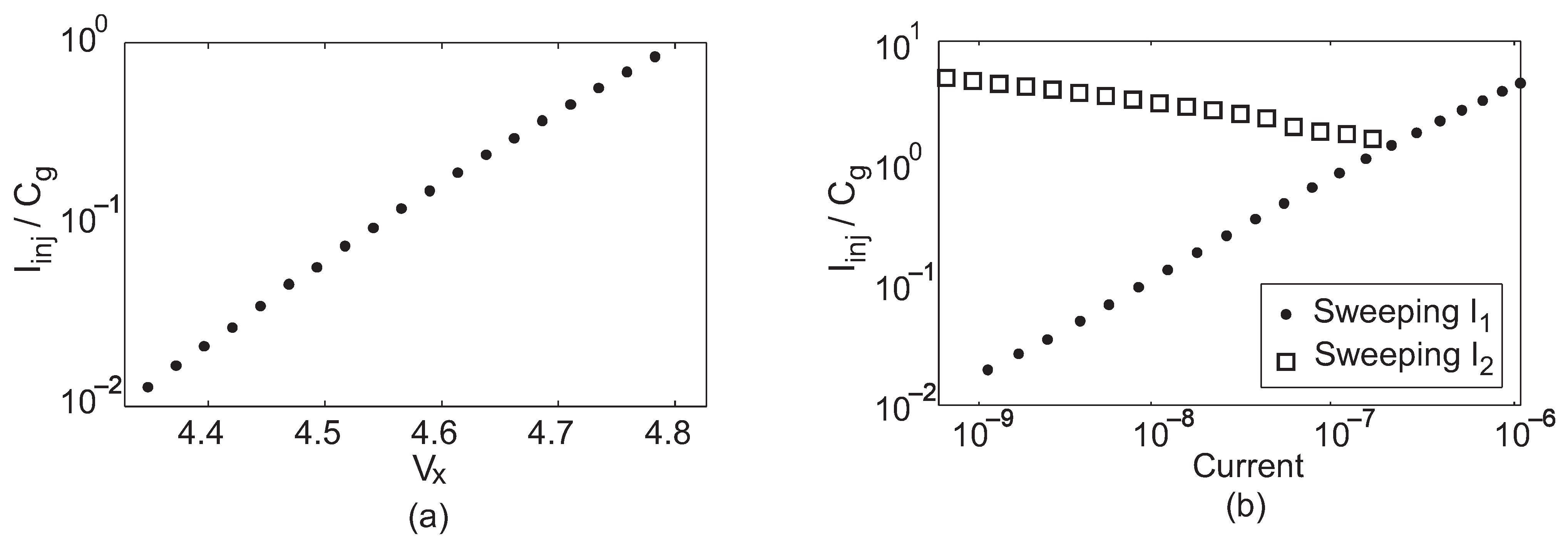
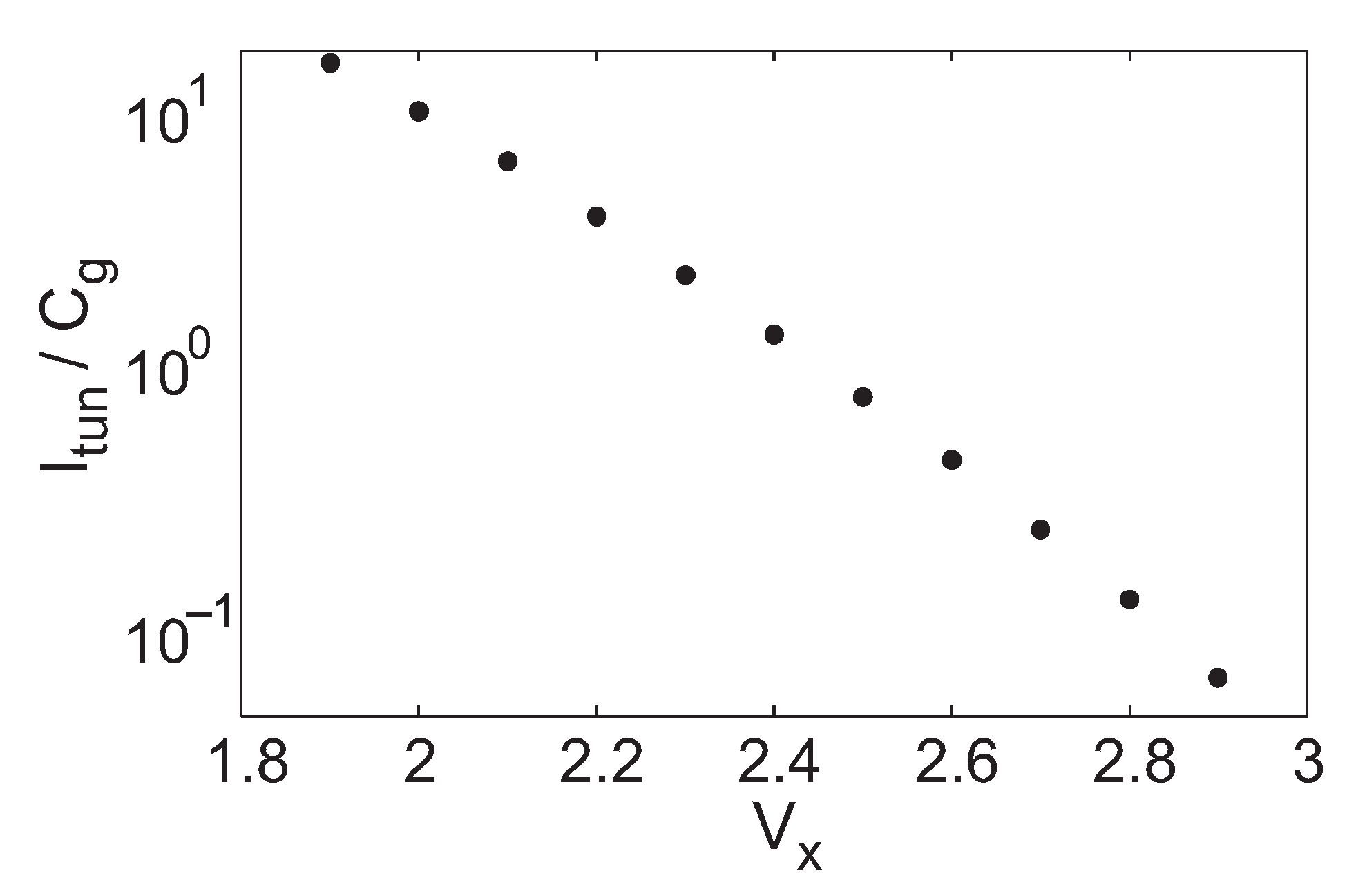
Figure 6 shows measured injection rates as a function of each of these control terminals. The injection rate was measured by determining the slope of
during injection experiments that were similar to the injection pane in
Figure 4; this slope is equal to the injection current normalized by the control-gate capacitance. When not being swept,
,
, and
were held fixed at 5 V, 860 nA, and 2 nA, respectively. Additionally, since the feedback holds
constant, this cell has linear tunneling characteristics.
Figure 7 shows the dependence of the tunneling current on
while all other terminals were held fixed.
The experiments shown in
Figure 6 and
Figure 7 demonstrate the ability to adjust the cell’s programming rate over a large range using either voltage or current inputs. Additionally, the weak dependence on
—approximately an inverse fifth root dependence—makes
appropriate for fine rate adjustment. Furthermore, the cell works well in the subthreshold region, where power consumption is low and Equation (
2) holds true.
5. Programmer Circuit
The combination of control terminals makes the memory cell very flexible in terms of creating a “programming circuit” to inject the memory cell to a desired value.
Figure 8 illustrates one possible programming circuit that uses
as the control terminal, and we will use this programmer circuit throughout the rest of this work. This programmer circuit consists of an operational transconductance amplifier (OTA) and a current mirror. In program mode, the programmer circuit is connected to the FG memory cell in the configuration shown in
Figure 8. The OTA converts the difference between
and a target value,
, into a current. This current is rectified by the current mirror
–
and is forced into the source terminal of the FG transistor. Accordingly, this current is able to precisely control the programming of the FG memory cell.
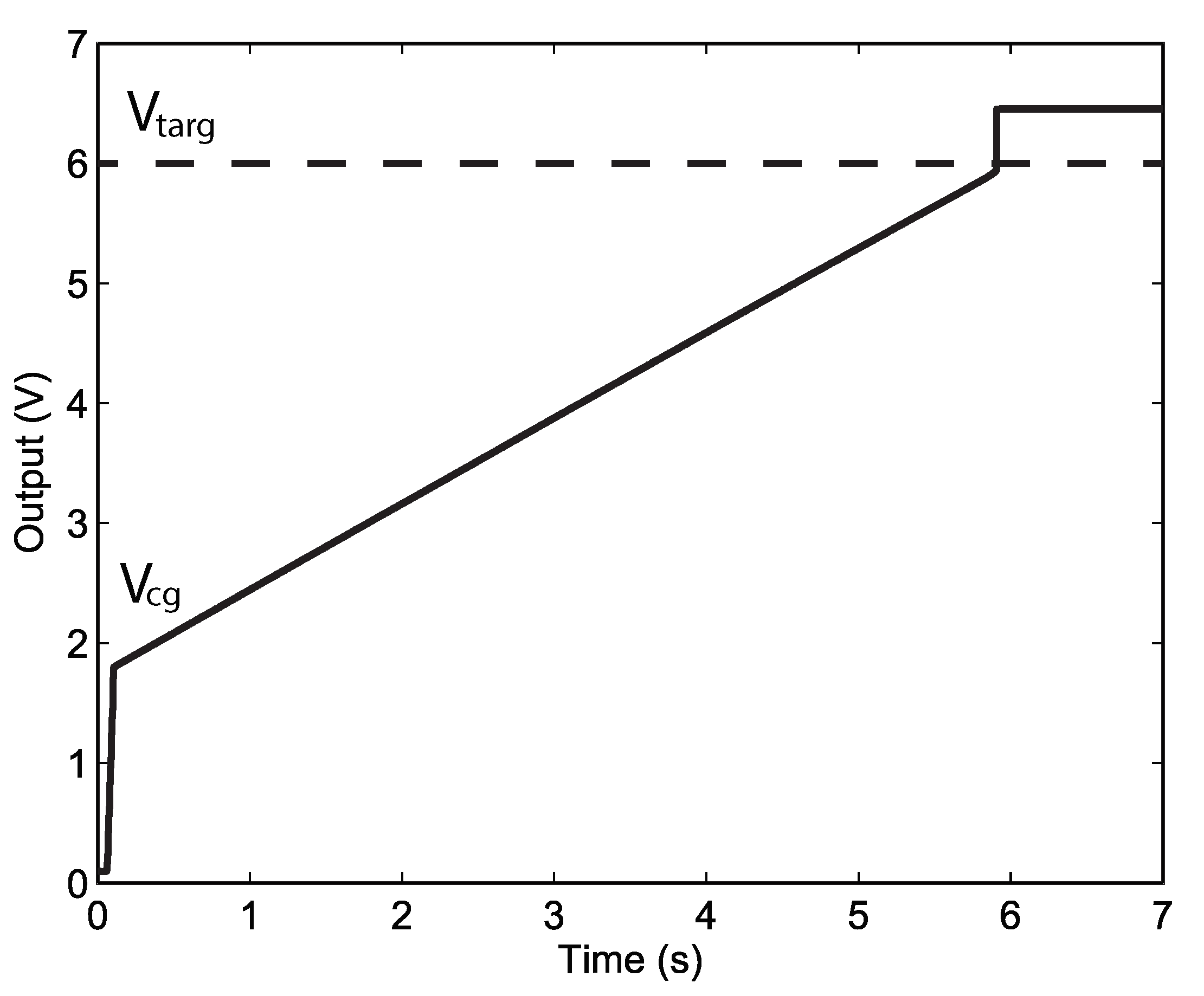
Figure 9 illustrates the programming procedure with measured data from an integrated circuit fabricated in a standard 0.5
m CMOS process. Prior to “writing” a value to the FG memory cell, the memory cell is erased by tunneling the FG transistor—a large voltage is applied to
until the control-gate voltage,
, of the FG memory cell drops to a voltage near ground. With
reduced to its run-time voltage and with
held at the nominal supply voltage, the value of
maintains a low (near-ground) voltage. This is the “erased” state of the FG memory cell.
To initiate injection, the supply voltage is ramped up to an elevated value,
, which pulls
up to a non-zero value. The exact value of
necessary for injection is process-dependent, and [
20] provides details on how this voltage changes with technology nodes. While
is well below the target value, the OTA output current is saturated, and the injection rate is constant because the current through the FG transistor is constant, while also maintaining constant voltages on the source, drain, and floating gate. As
approaches
, the OTA enters its linear input range, and the current in the FG transistor becomes proportional to the difference between
and
. Consequently, as the target is approached, the injection rate is reduced, and eventually stopped, by the reducing
. When
shuts off, the current conveyor structure stops operating, and
is pulled high. At this point, injection no longer occurs. The FG memory cell and programmer have their supply voltage lowered to the nominal
, and programming of the FG memory cell has been completed.
After injecting the FG memory cell, it is placed in read mode by disconnecting it from the programmer OTA and current mirror—i.e., it is configured as
Figure 5. The cell’s voltage output is read from
while constant currents are applied to
and
.
Alternatively, the FG transistor can be disconnected from the rest of the memory cell for current readout mode. In current readout mode, is connected to a fixed potential, the source of is connected to , and the drain is connected directly to the circuit that it biases. In short, is configured as a current source, with the exact value of current dependent on the charge programmed on the FG.
The combination of this programmer circuit and the FG memory cell is able to provide a linear mapping between the target voltages (
) and the output voltages (
) of the memory cell after being programmed.
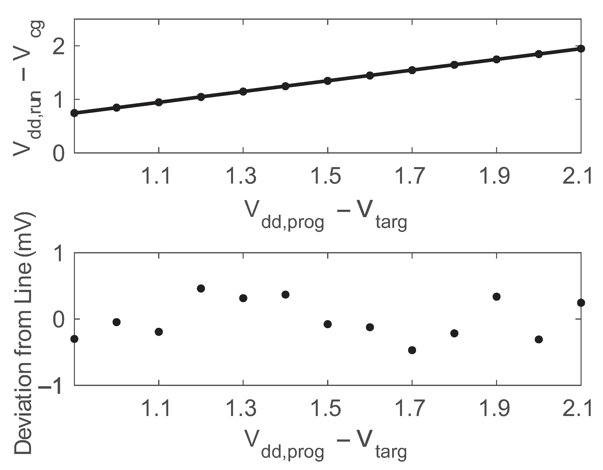
Figure 10 shows the measured relationship between the target voltages and the corresponding output voltages after the FG memory cell has been disconnected from the programmer and the supply voltage has returned to the nominal
. These measurements were taken from an integrated circuit fabricated in a standard 0.35
m CMOS process. As can be seen, linearly spaced target voltages result in linearly spaced output voltages. The bottom pane shows the deviation from a straight line with a slope of 1.0025 (the linear fit to the data). Over a target range of 0.9 V–2.1 V (1.2 V total), the worst-case deviation from the straight line was only 0.49 mV.
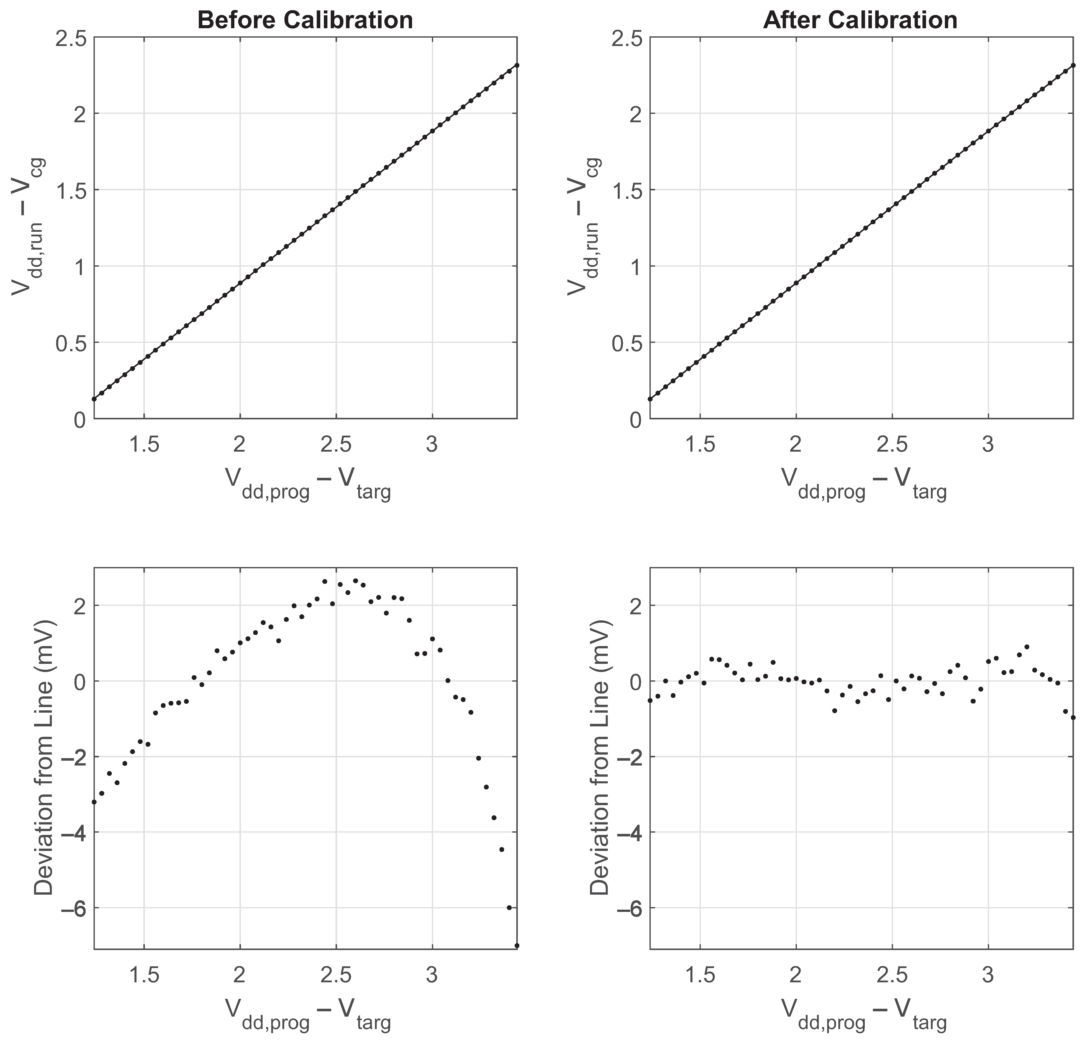
The programmer/memory-cell combination is capable of programming to a larger range of voltages, but the relationship begins to deviate slightly from a straight line with a larger
range.
Figure 11 shows the
to
relationship for a voltage range of 2.2 V. The
values deviate as much as 7 mV from the ideal straight line. However, a simple calibration step can be used to correct for these deviations from the straight line. The curvature of the output
values has an approximately third-order relationship. Therefore, using a third-order polynomial to calibrate the
to
relationship results in a worst-case deviation of 0.9 mV from a straight line, as is shown in
Figure 11.
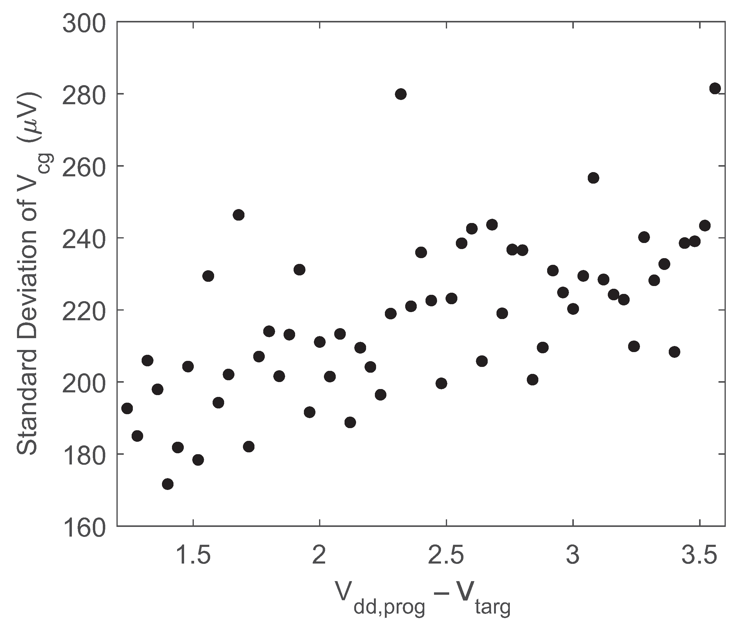
To verify the repeatability and precision of the programming process, the memory cell was programmed using the programmer circuit for linearly spaced values of
. The FG memory cell was programmed 100 times to each target value ranging from 1.24 V−3.56 V (2.32 V total range), with a full erasure after each write/measurement. Each programming cycle was 100 ms in duration and used
V.
Figure 12 shows the standard deviation of the 100 measurements of
for each
, which had a worst-case value of 280
V. Using the worst-case standard deviation of the repeatability measurements as the minimum detectable change that can be distinguished over the 2.32 V range, then this FG cell/programmer combination is capable of 13.0 bits of resolution when programming.
Previous work in similar technology nodes has shown that charge retention after programming is very good (e.g., [
21,
22,
23]), with results indicating that 10-year lifespans can be achieved from FG memory for analog applications with little charge loss. For example, ref. [
23] has shown drift of less than 0.5
V over 10 years at room temperature, which is sufficient for maintaining the 13.0 bit resolution in our system. One item that should be pointed out is that high fields through the oxide due to tunneling and injection can cause some damage to the oxide and also result in charge trapped in the oxide. However, in contrast to digital systems in which nonvolatile memory undergoes frequent write/erase cycles, nonvolatile analog memory write/erase cycling is often quite sporadic in comparison—with nonvolatile analog memory having a spectrum of needs in terms of the frequency of write/erase cycles. At one end of the spectrum of nonvolatile analog memory applications, the FG device only needs to be programmed once to account for process variations, biasing conditions, and/or mismatch compensation. In these cases, the nonvolatile memory does not need to undergo any extra write/erase cycles, so damage to the oxide will be inconsequential. Even at the other end of the spectrum where applications require more write/erase cycles, the frequency of write/erase cycling is still likely dramatically less than in digital systems, so it is likely that these systems will not undergo significant stresses either. However, if they do suffer some effects of oxide degradation and/or charge trapping, then the calibration curve from
Figure 11 can be retaken periodically to reassess the target values needed to achieve the desired accuracy from the system. Analysis of long-term retention and effects of charge trapping in nonvolatile analog memory is ongoing research work and will continue to be studied in further detail. Because of the varied needs of programming nonvolatile analog memory in terms of how fast and how often they need to be programmed, we provide two methods for programming arrays of FG transistors in the next Section—(1) serial programming for area-constrained systems that do not need frequent re-writes and (2) parallel programming for systems that either need frequent re-writes or cannot handle long outage times during write/erase cycling.
Since the main application of the FG memory cell introduced here is to be used in low-power analog systems, the power dissipation of the memory cell in run mode should be small. In voltage readout mode, the cell in
Figure 5 was biased with
nA and
nA, yielding a low power consumption of 66 nW/cell. If the FG transistor is configured for current readout, then the current is part of the circuit that it is biasing and does not contribute any additional power consumption beyond that of the circuit.
6. FG Array Programming
Since a benefit of FG transistors is that they allow for dense memory arrays, we employed our FG memory in several analog memory arrays. In an array configuration, FG memory cells are arranged in M rows by N columns, depending on the size of the application. Multiplexing circuitry at each of the FG memory-cell terminals is used to select/deselect cells and to apply the required voltages for the read/program processes.
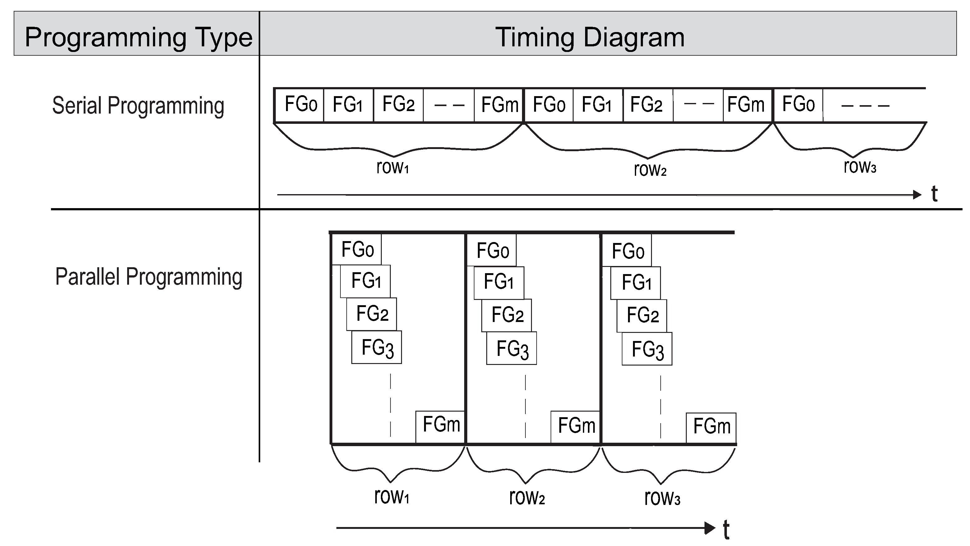
The two main methodologies for programming an array of FGs are serial and parallel programming. As their names imply, serial programming involves programming one floating gate at a time, while parallel programming involves programming multiple floating gates simultaneously. Serial programming is suitable for applications where the chip area is constrained, since only one programmer circuit is required for the entire chip. On the other hand, parallel programming is preferable for analog applications that require faster write times for a large number of FGs; however, parallel programming requires larger area overhead for additional programming circuitry. We will discuss these two programming methodologies in the following subsections.
6.1. Serial Programming of FG Arrays
In serial programming, FGs are programmed one transistor at a time. Therefore, only one programmer circuit is needed per chip, which helps to keep the infrastructural circuitry compact. During injection, one specific FG cell is selected and connected directly to the programmer circuit of
Figure 8. When the supply voltage is elevated to a voltage large enough to induce injection, which we will denote as
, injection starts, and only the selected FG memory cell is injected. All unselected FG memory cells are configured to prevent injection by pulling the unselected cells’
to
and by setting the drain-to-source voltage,
, of the FG transistor to be low (
V) by connecting the source and drain to ground. Once the selected FG memory cell is injected to the desired target, it is disconnected from the programmer and a new FG memory cell is selected and connected to the programmer circuit. The process is repeated for each of the FG memory cells needing to be injected.
Since only one programmer circuit is used in serial programming,
programming cycles are required to program an
array. For large arrays, the
programming cycles could cause a significant unwanted down-time in which the system is not operational while it is being programmed, which could also be impractical for large arrays that require frequent reprogramming. However, not all applications require constant up-time or frequent rewrites. For example, in [
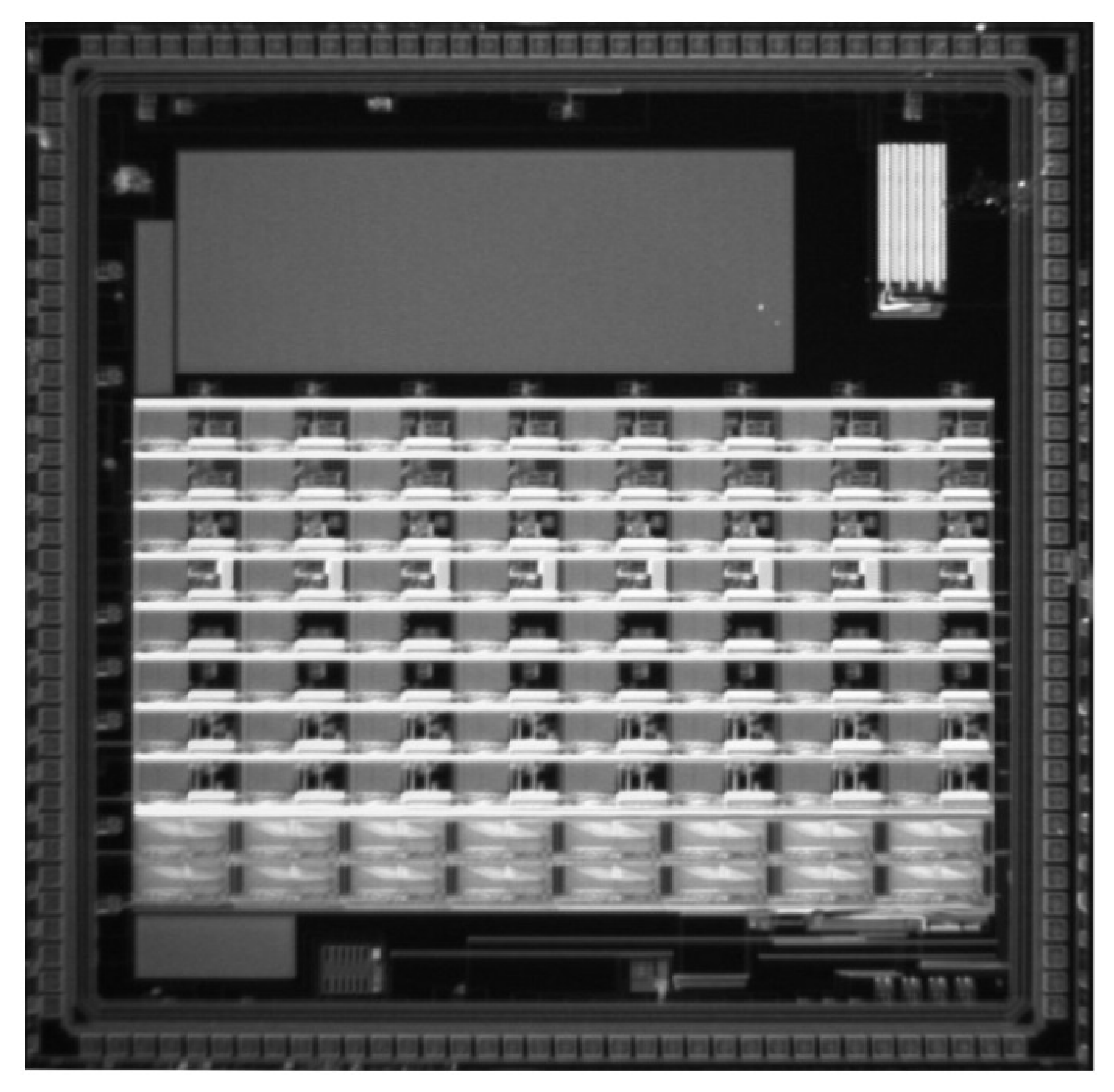
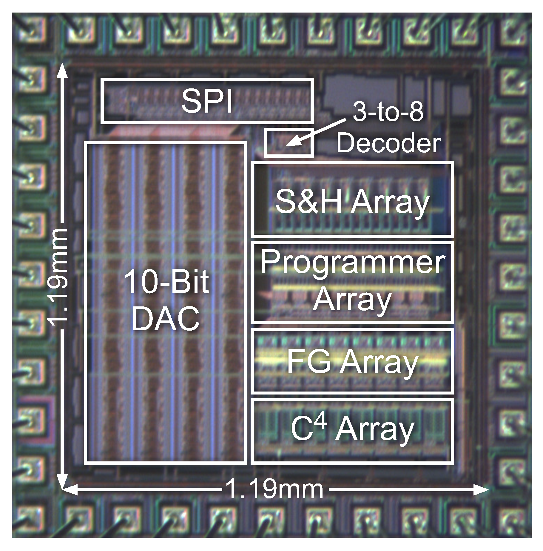
1], the serial programming method was used to program the FG transistors on a reconfigurable analog processor. A die photograph of this programmable analog system is shown in
Figure 13.
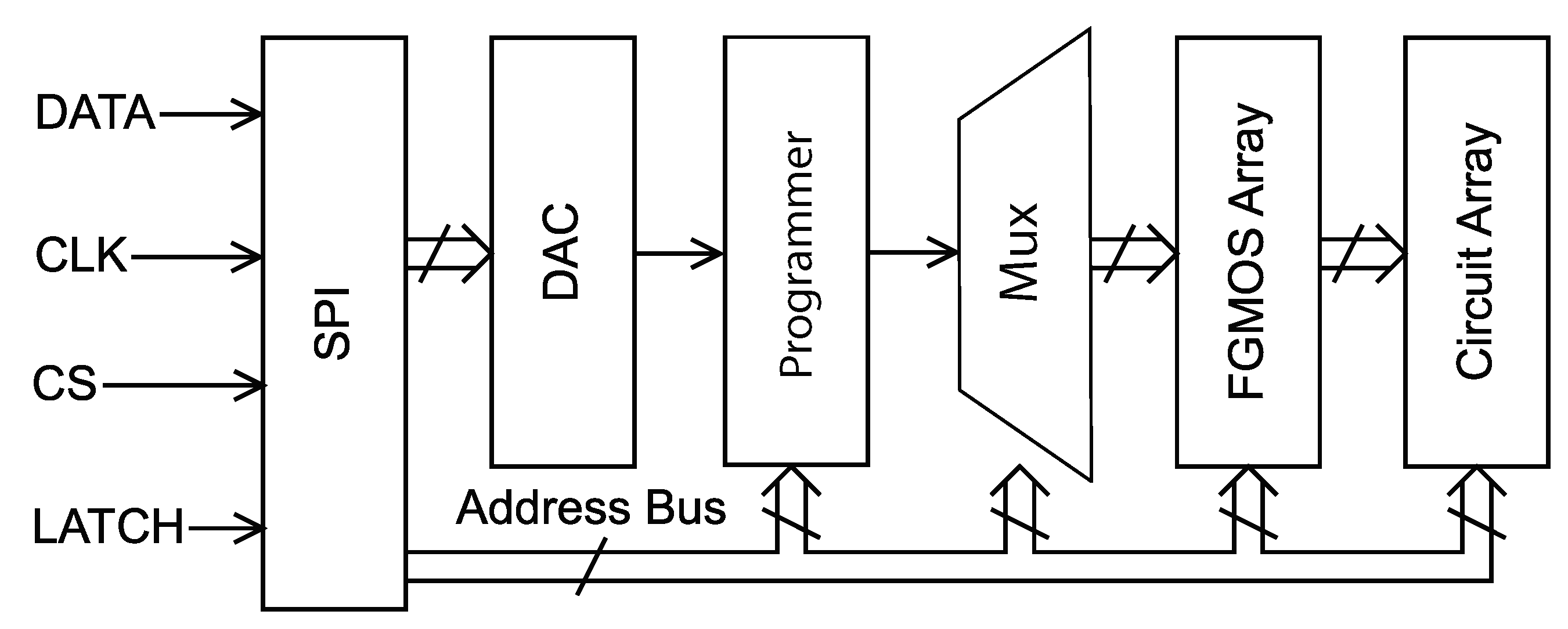
A signal-flow block diagram of the serial programming method is shown in
Figure 14. A serial peripheral interface (SPI) is used to select the particular FG memory cell to be programmed, connect the programmer circuit to the appropriate cell, enable read/write mode, and control a voltage scaling digital-to-analog converter (DAC) to apply the desired target voltage. The programming process for this scheme operates as follows:
Globally erase all floating gates using tunneling
Raise the supply voltage to its elevated injection level
Set the DAC output voltage () and select a specific row/column combination
Connect the programmer circuit to the corresponding FG memory cell
Programming starts immediately—hold for approximiately 100 ms to ensure that injection completes—injection will automatically shut off when the FG memory cell reaches the desired target
Repeat steps 3–5 for all FG memory cells in the array that need to be injected, one at a time
Lower the supply voltage to when all FG cells have been programmed
6.2. Parallel Programming of FG Arrays
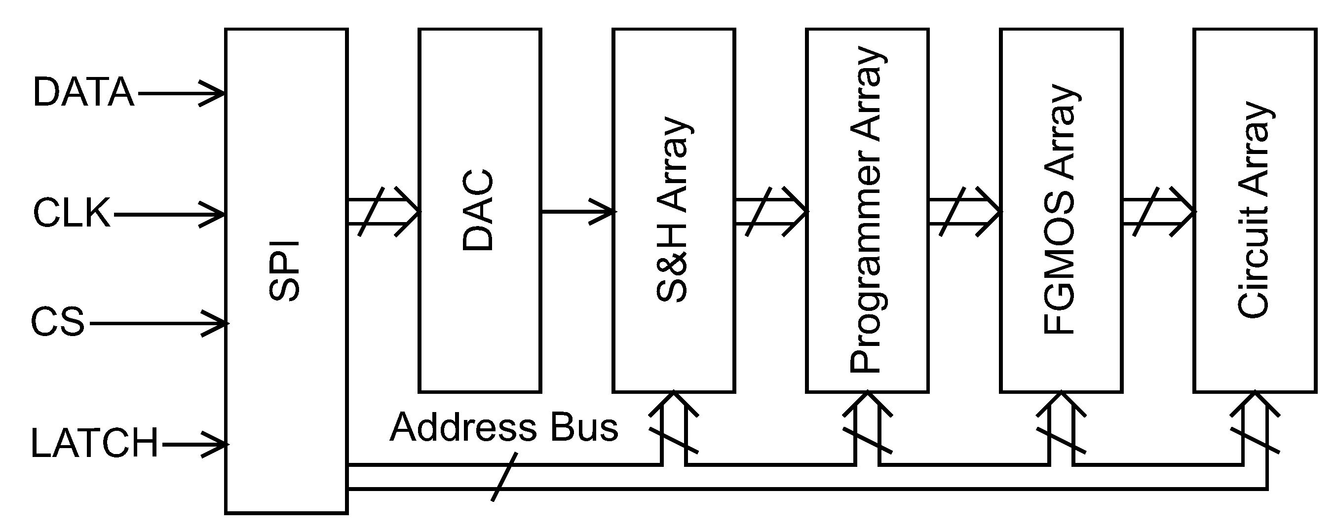
To accelerate the process of programming a large number of FG cells, a parallel programming technique can be used. In parallel programming, more than one cell is programmed at a time. Consequently, multiple programmer circuits are required per chip to accomplish parallel programming and will result in faster programming, since one programming cycle is able to program multiple FGs in the array. However, in order to program X floating gates in parallel, there must be X programmer circuits available—one for each FG that will be programmed simultaneously. In this subsection, we present an FG array with a parallel programmer scheme. In this particular system for an array, N programmer circuits are used—one for each column.
A block diagram of the whole parallel programming system is shown in
Figure 15. Like with the serial programming system, a digital interface for programming via SPI is used to set all parameters needed for programming. Consequently, only four digital input signals are required to program the full array of FG memory cells, which minimizes the number of pins required to interface with the chip, reduces programming overhead, and removes some of the programming details from the end user.
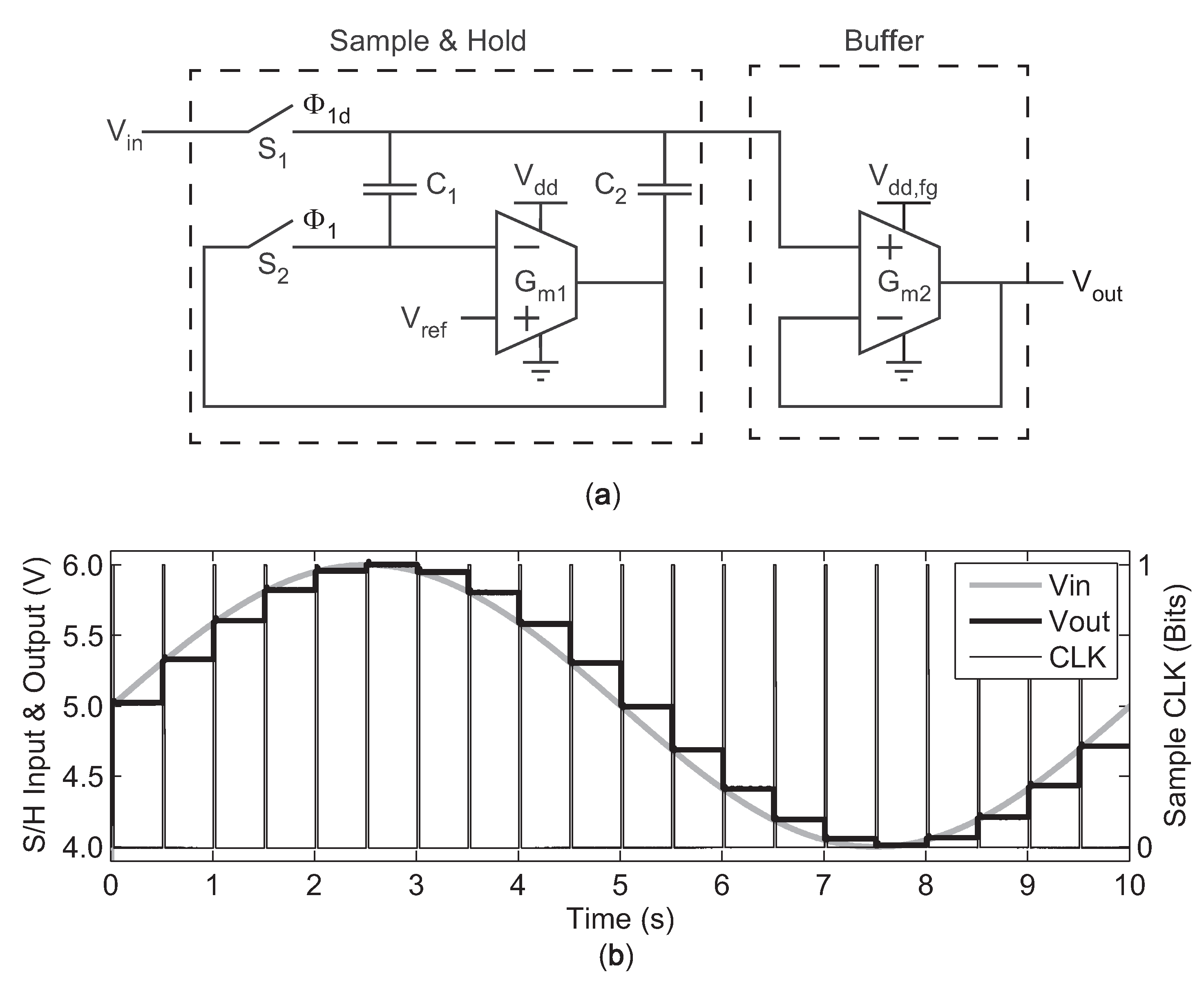
A voltage-scaling DAC is again used to generate analog target voltages. However, differently from the serial programming scheme, the output of the DAC is sampled by an array of sample-and-hold (S/H) circuits which provide the actual target voltages that are applied to the array of FG memory cell circuits to perform programming. This array of S/H circuits permits one single DAC to be used instead of N DACs for each FG memory cell being programmed in parallel. The DAC is stepped through N different values, and each of the N outputs are sampled—one output by each S/H circuit. These N voltages are held at the outputs of the S/H circuits (i.e., values of each of the N programmer circuits) until all N FG memory cells are programmed.
The requirements of the S/H circuits used in this application are that they must have long hold times to reliably maintain a constant target voltage while all N FG memory cells are programmed in parallel. Additionally, the S/H should have low pedestal error so as to not introduce offset between the DAC and the individual values.
To achieve the long hold times and low pedestal error, we employed a S/H topology based on [
24]. This S/H employs Miller feedback in its hold-mode configuration to increase the effective hold capacitance,
, without requiring larger drawn capacitors. This configuration reduces the droop rate of the S/H. A simplified version of the S/H schematic is shown in
Figure 16a. The two switches,
and
, are comprised of transmission gates which include half-sized dummy transmission-gate switches on each node except for
, since this charge injection error gets absorbed by the input source and does not affect
. Also, note that switch
is clocked using
, a delayed version of
. Consequently,
opens slightly before
when transitioning to hold mode, further reducing charge injection [
25].
In sample mode, the S/H OTA,
, is connected as a unity-gain buffer, forcing its inverting input to equal
as
and
are charged to
. In hold mode,
and
are opened, and Miller feedback through
and
forces the capacitance on the hold node to be
, where
A is the open-loop gain of the S/H OTA,
.
Figure 16b demonstrates the S/H’s operation by showing a transient plot of the S/H sampling a sine wave. The time scale is large, illustrating the long duration of hold times achievable by this circuit (hold time of 500 ms in this example).
The addition of the S/H array necessitates extra considerations to initiate injection in each device. Before programming, the output of the DAC is forced to ∼0 V. Each S/H is sequentially selected, and ∼0 V is sampled onto each of them. Next, the supply voltage of the buffer OTA,
, is raised to
(note that
does not need to be raised up to the higher supply voltage), and each FG in row
M is connected to its corresponding programmer. Since a low
was set for each programmer, all of the FG memory cells connected to the programmers have their
latched to a high voltage, and no FG memory cell undergoes injection. The DAC then sequentially applies the desired
for each FG memory cell. However, injection still does not happen because
is still latched high. To initiate injection, an extra switch is connected to the output of the programmer OTAs of
Figure 8. A short-duration “start” pulse briefly shorts the output of the OTAs to ground, causing current to flow in the current mirrors biasing the FG transistors. This current resets the
values of the memory cells to a low value. At the conclusion of the start pulse, the FG memory cells inject to the targets. Once the last programmer has started injecting its FG memory cell, the supply voltage is left at a high value of
for a set period of time to ensure that all FGs have reached their targets.
Figure 17 shows the die photograph of an example system employing parallel programming of an array of FG memory cells. This integrated circuit was fabricated on a standard 0.5
m CMOS process, and system-level results from this integrated circuit will be shown in the following Section.
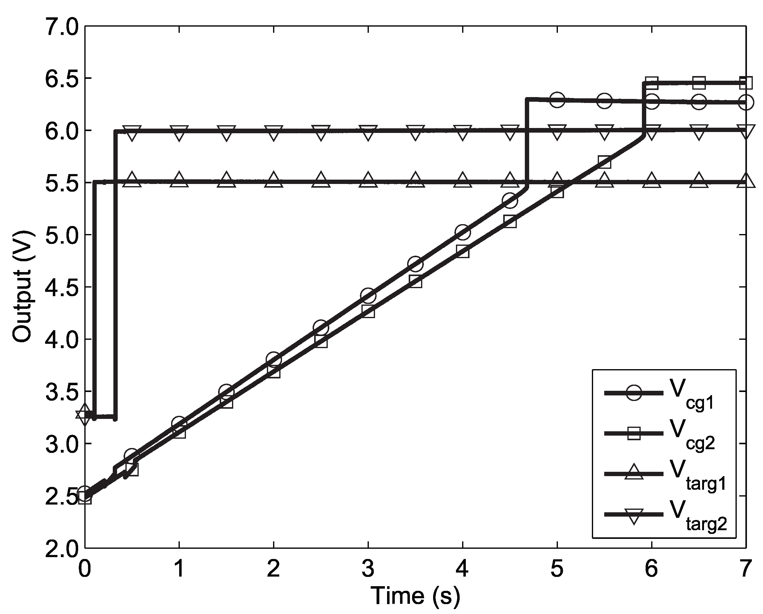
Figure 18 shows two FG memory cells on this chip being programmed in parallel using our programmer. Note that while 8 memory cells are programmed in parallel on this chip, the voltage outputs of only two cells were observable at any time—one was observable via selection by the the SPI, and another was hard-wired to output pins for debugging purposes. In this Figure at 100 ms, the first S/H is clocked, sampling the DAC output to set
. Shortly after, the start pulse is applied to initiate injection. Then, the next column is selected, and the process is repeated. A very long programming time-scale is shown in this example to illustrate the long hold times available by the S/H circuitry. However, typical programming hold times are 100 ms.
A summary of the parallel programming procedure is as follows:
Globally erase all floating gates using tunneling
Sample ∼0 V on each of the S/H circuits
Raise the supply voltage to its elevated injection level,
Set the DAC output voltage and select a specific row/column combination
Sample the target voltage from the DAC to set
Initiate injection with the start pulse
Repeat steps 4–6 for each subsequent FG memory cell in the column
Repeat steps 4–7 for each row in the array
Lower the supply voltage to when all FG cells have been programmed
6.3. Serial vs. Parallel Programming
As a comparison between the two methods for programming arrays,
Figure 19 demonstrates the programming time for serial and parallel programming. As the Figure illustrates, to program an array of FGs serially, one FG is programmed at a time, which makes the programming process linearly proportional to the overall size of the array. Using the serial method for programming results in overall programming time of:
where
M is the number of rows,
N is the number of columns,
is the injection time, and
is pre-injection time (time to select the FG cell, connect the programmer, and apply the start pulse if needed) which is very short compared to
. On the other hand, our parallel programming method dramatically reduces the overall programming time by staggering FG programming through time, as shown in
Figure 19. To program an
array using our parallel programming method, the overall programming time is:
Generally, comparing the two methods, our parallel programming compromises between minimizing die area (by using a programmer circuit per each column) and programming time, which makes it the most appropriate programming method for FG-dense analog applications. Serial programming is most appropriate for systems that are size-constrained and/or can handle longer down times between write cycles.
7. System Application
FG transistors have a wide range of analog applications that require a large number of FGs to be integrated on a single die. These applications range from simple filter banks to more complicated field-programmable analog arrays (FPAAs). FGs are used to provide biasing voltages/currents for those analog applications. A proof-of-concept system was fabricated in a standard 0.5
m CMOS process, and it consists of a programmable filter array employing our parallel programmer. This chip contains 8 sample-and-holds, 8 programmer circuits, a
array of floating-gate transistors (16 total), and 8 bandpass filters. This chip also contains the SPI, DAC, and miscellaneous peripheral circuitry. Each bandpass filter requires two FGs for biasing—one for the low corner frequency and one for the high corner frequency. The FGs are distributed in an array of 2 rows and 8 columns. In this configuration, the chip allows for one row of FGs to be programmed in parallel. Thus, two programming sequences, one for each row, are required to program the full chip. A die photograph of the chip is shown in
Figure 17.
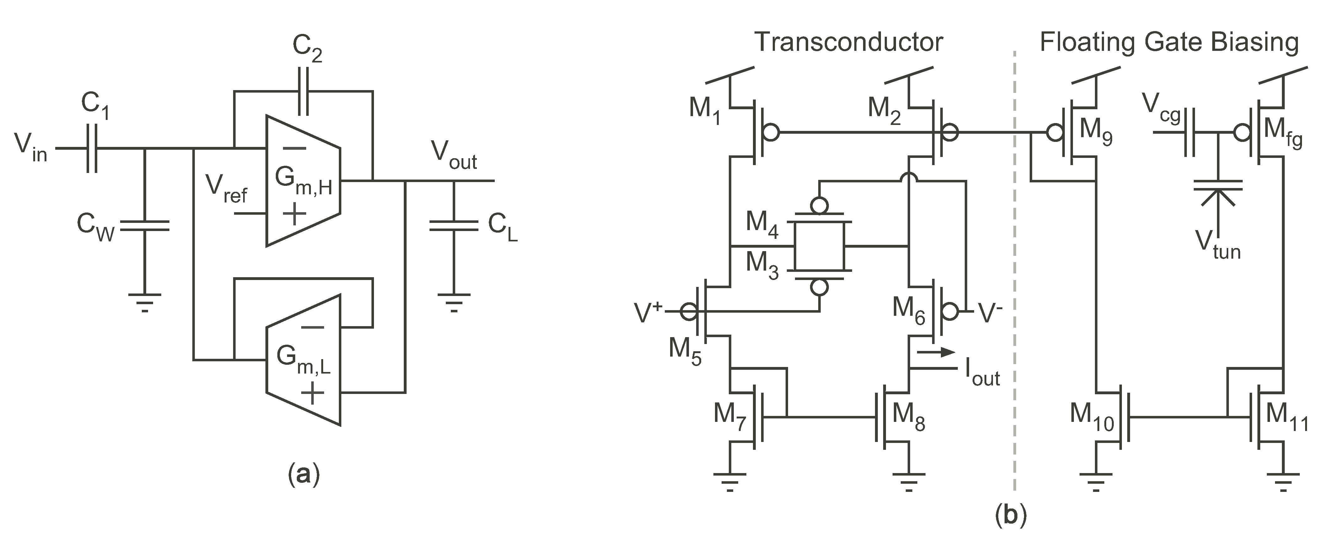
To demonstrate the programmer’s ability to directly tune circuit parameters, we use the capacitively-coupled current conveyor (
) presented in [
4] and shown in
Figure 20a. The
is a transconductance-capacitance (
-
C) filter whose corner frequencies are proportional to the transconductances of two OTAs—
and
in
Figure 20a. Since these transconductances are directly proportional to the bias currents of each OTA, the corner frequencies can be directly tuned using the FG memory cell as a current reference to bias them.
Figure 20b shows how the FG transistors are configured as current sources and are connected to the OTAs.
Figure 21a shows the effect on frequency response holding
constant and programming different values of
;
Figure 21b shows the effect of increasing
. As can be seen, the two corner frequencies can be tuned orthogonally, so that the current in one OTA does not impact the corner frequency set by the other OTA. In this example system, the biases providing the low corner frequencies for each of the bandpass filters were contained on one row (and programmed simultaneously), and all the biases for the high corner frequency were on the other row.
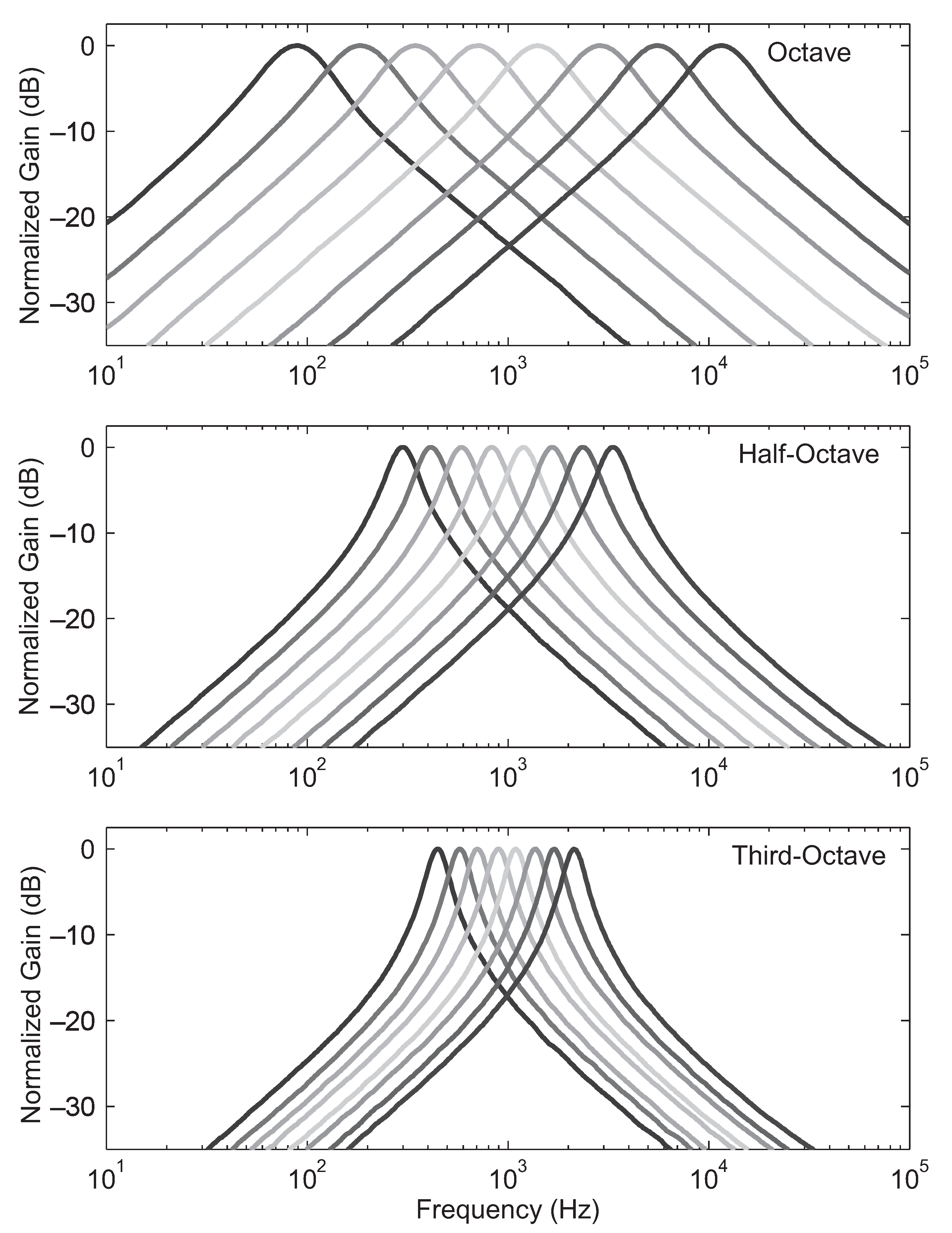
Figure 22 demonstrates the capability of accurately programming the parameters of a filter array using the parallel programming structure presented in this paper. Three filter spacings are demonstrated: full-octave spacing, half-octave spacing, and third-octave spacing. The value of the quality factor,
Q, for each of these configurations was chosen according to fractional-octave spacing rules, such that the filters cross at their
dB points. Therefore,
Q∼1.4 for octave spacing,
Q∼2.9 for half-octave spacing, and
Q∼4.3 for third-octave spacing.
Figure 22 (top) shows the results of programming the
s to octave spacing starting at
Hz,
Figure 22 (middle) shows half-octave spacing beginning at
Hz, and
Figure 22 (bottom) shows third-octave spacing beginning at
Hz.
As can be seen from
Figure 22, the programming structure presented in this paper is able to precisely tune the circuit parameters to achieve exponentially spaced center frequencies. Additionally, the use of FG transistors provides a mechanism to tune the circuit’s operation for multiple conditions (e.g., different center frequency spacings, bandwidths, etc.).
8. Conclusions
We presented a compact analog FG memory cell that uses a continuous-time programming technique. Two different integrated circuits with memory cells and the programmer have been fabricated to characterize the design—one in standard 0.35 m CMOS with serial array programming and the other in standard 0.5 m CMOS with parallel programming. The FG memory cell and the programmer circuit were characterized and tested for repeatable programming. We demonstrated that the FG memory cell could be programmed to have a linear relationship with a target voltage over a range of 2.32 V with a resolution of 13.0 bits, all while being programmed in under 100 ms.
The FG memory cell was used to build a memory array that can be used in analog applications. A parallel programming technique was presented that significantly reduces the time required to inject all FG cells in the array. Finally, as a proof of concept, the FG memory array was used as programmable current sources to program a bandpass filter array.
Arrays of this FG memory cell are ideally suited to low-power applications that require analog processing of information—particularly applications that pre-process sensor information to make early classification and detection of events, such as [
26]. Either a serial or parallel programming paradigm, as described in this paper, could be used, and the determination between the two should be made based on area constraints, allowable duration of down-time while reprogramming, and frequency of write/erase cycles. Future work in the area of programmable non-volatile analog memory will include (1) circuits to linearize the
to
transfer function better to reduce the need for a calibration phase, (2) circuitry to permit negative voltages to be used in the injection process to eliminate the need for a voltage ramp-up phase for injection (early work has been presented in [
27]), (3) infrastructural circuits to support generating the write/erase cycles, (4) demonstration of performance in newer technology nodes, etc.


