
Silicon-Compatible Memristive Devices Tailored by Laser and Thermal Treatments

 , , , , , ,
Abstract
:1. Introduction
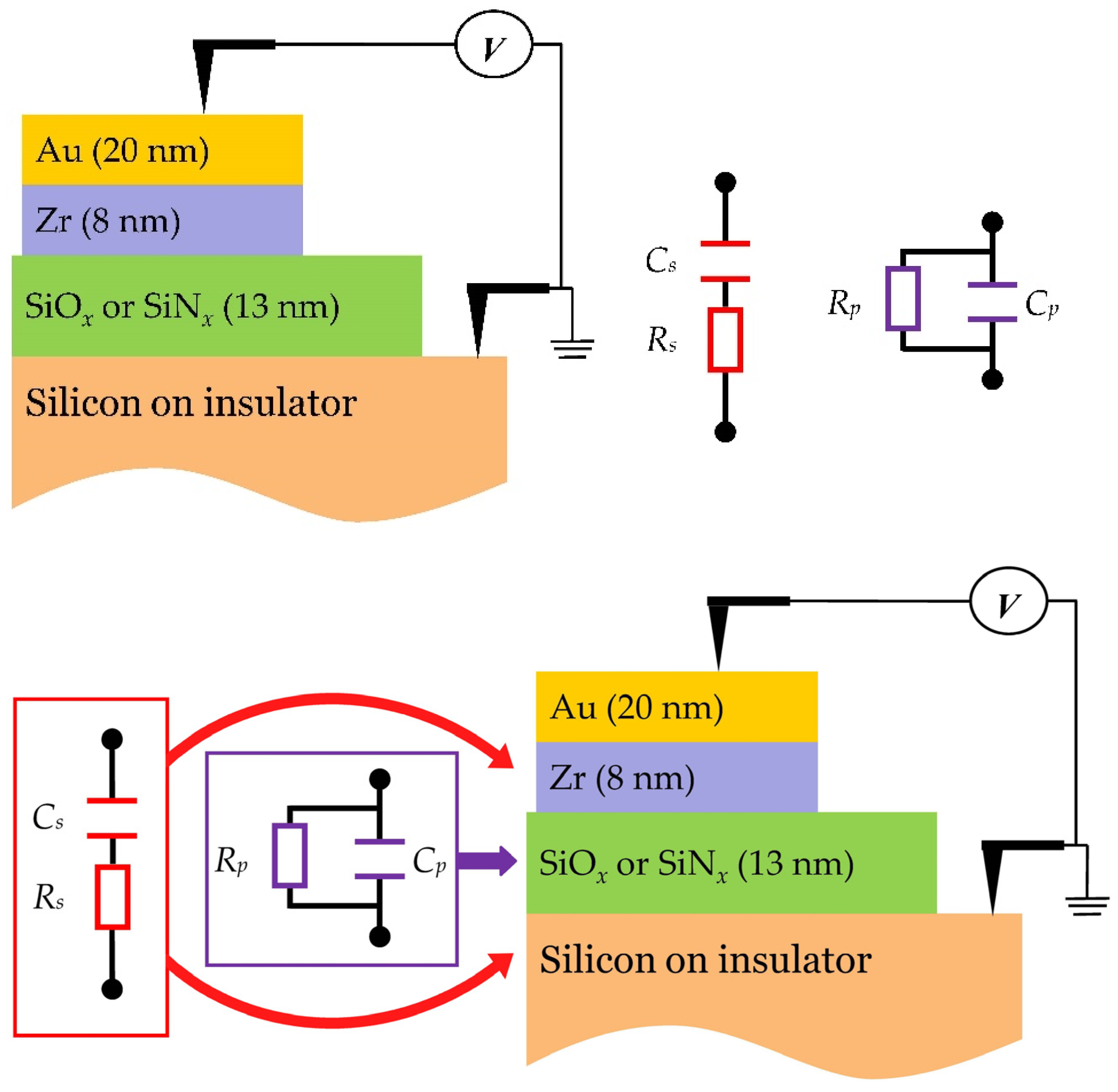
2. Materials and Methods
- SiOx—using 5% SiH4/N2 (160 sccm), N2O (1500 sccm) and N2 (240 sccm) at a pressure of 550 mTorr and high frequency (HF) power of 60 W, with a deposition rate of 200 Å/min;
- SiNx—using 5% SiH4/N2 (800 sccm), NH3 (10 sccm) and N2 (1200 sccm) at a pressure of 580 mTorr and HF-power 60 W, with a deposition rate of 100 Å/min.
3. Results and Discussion
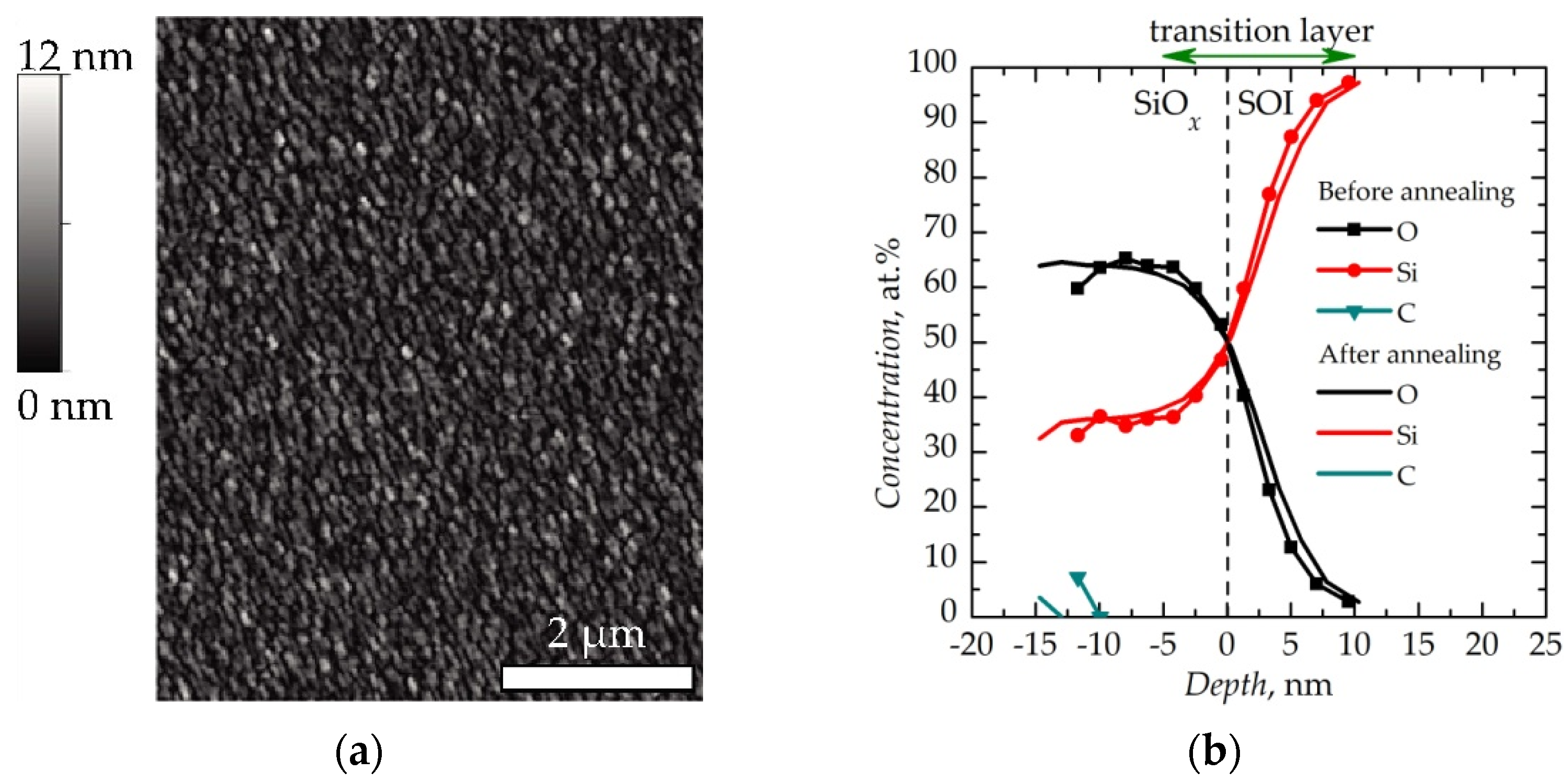
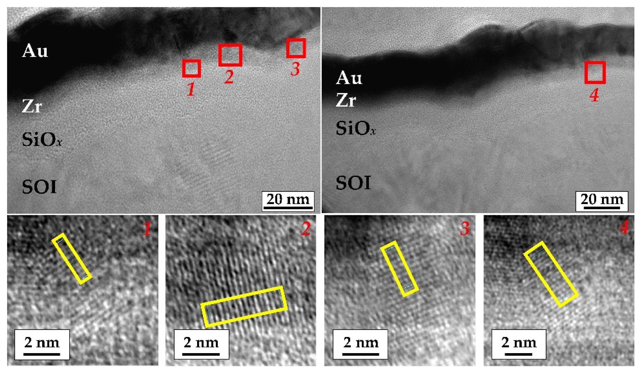
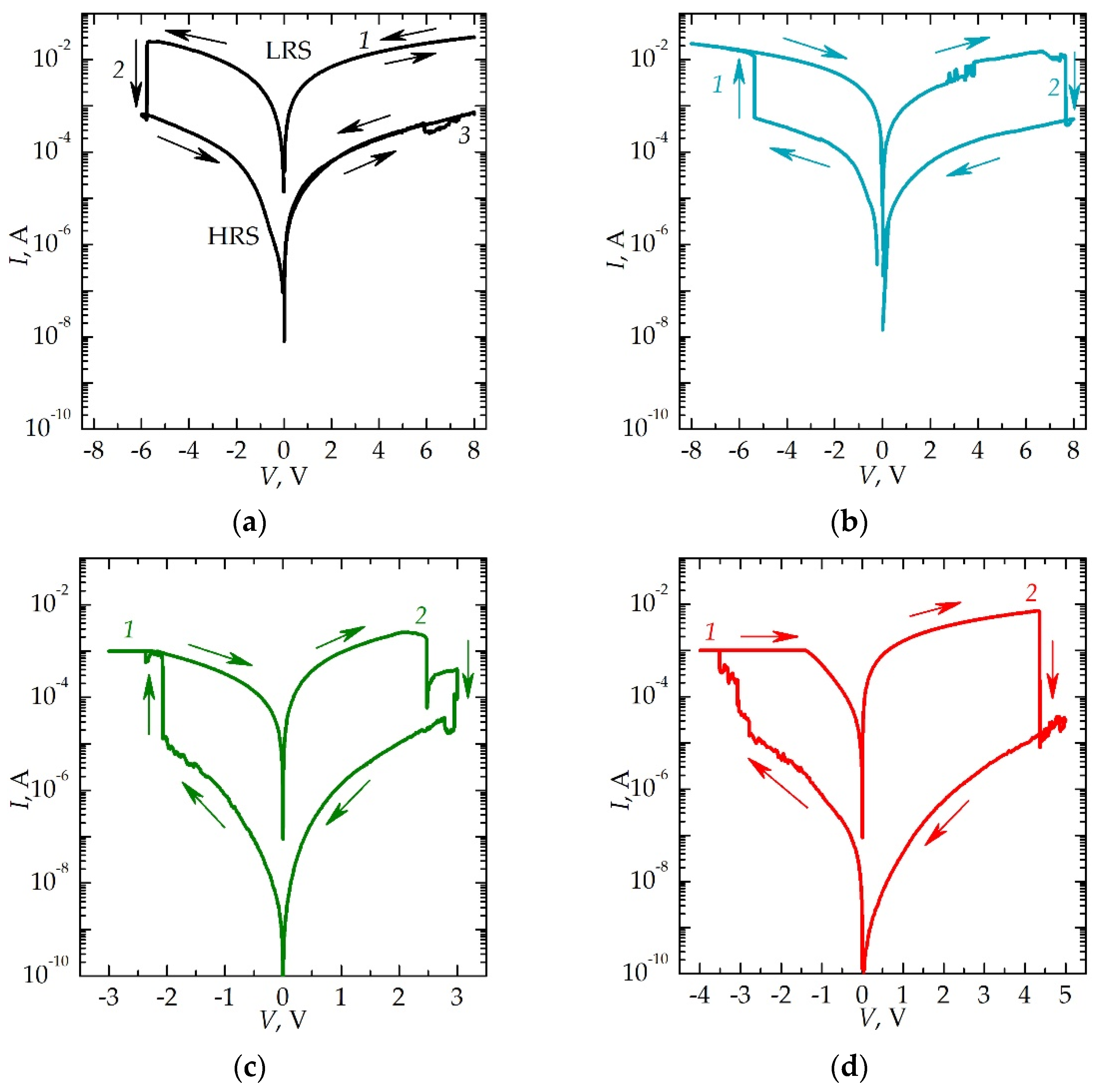
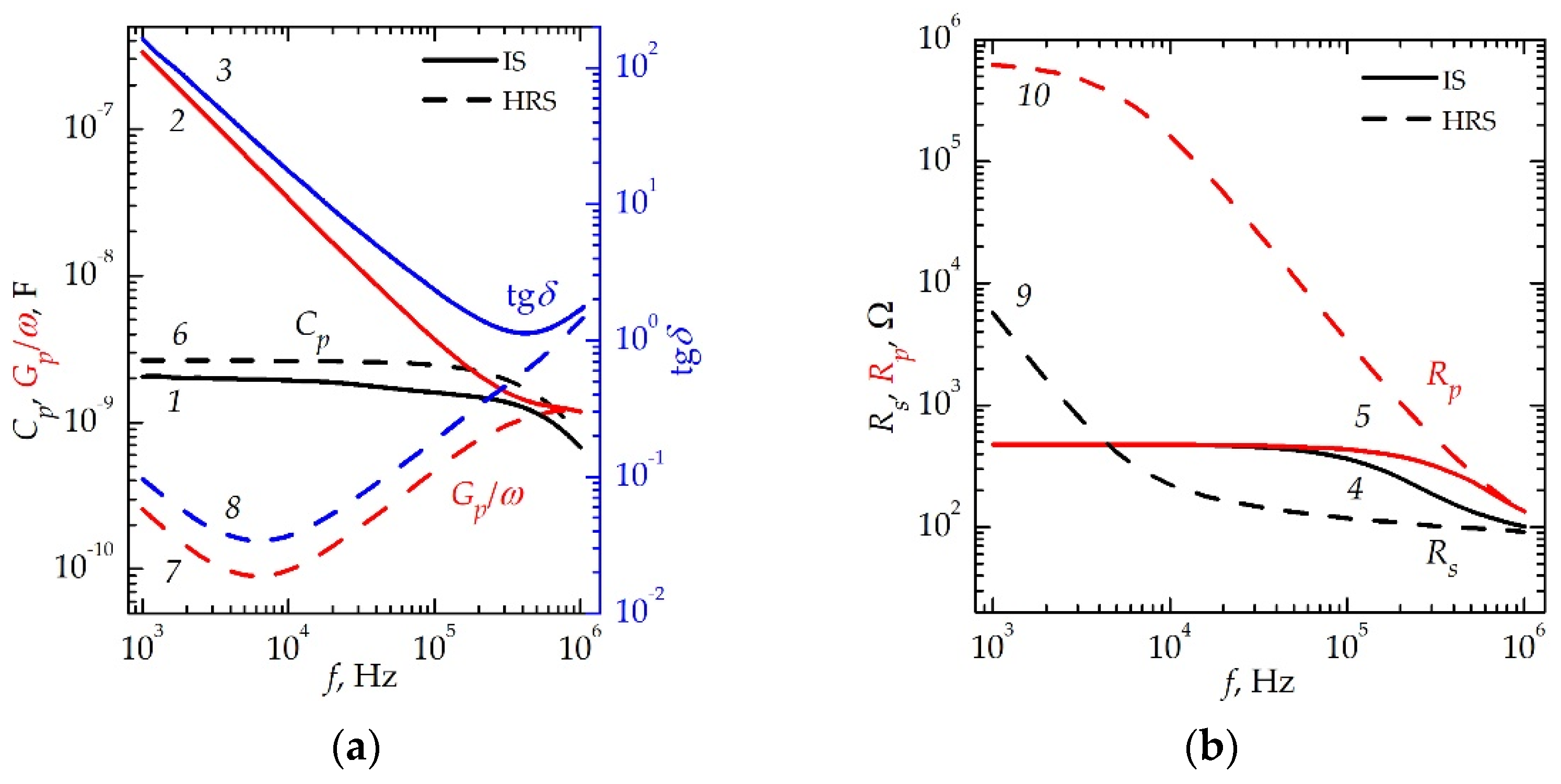
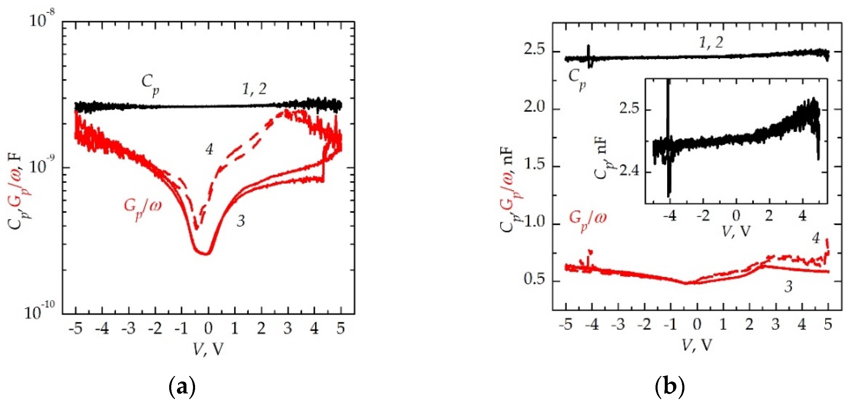
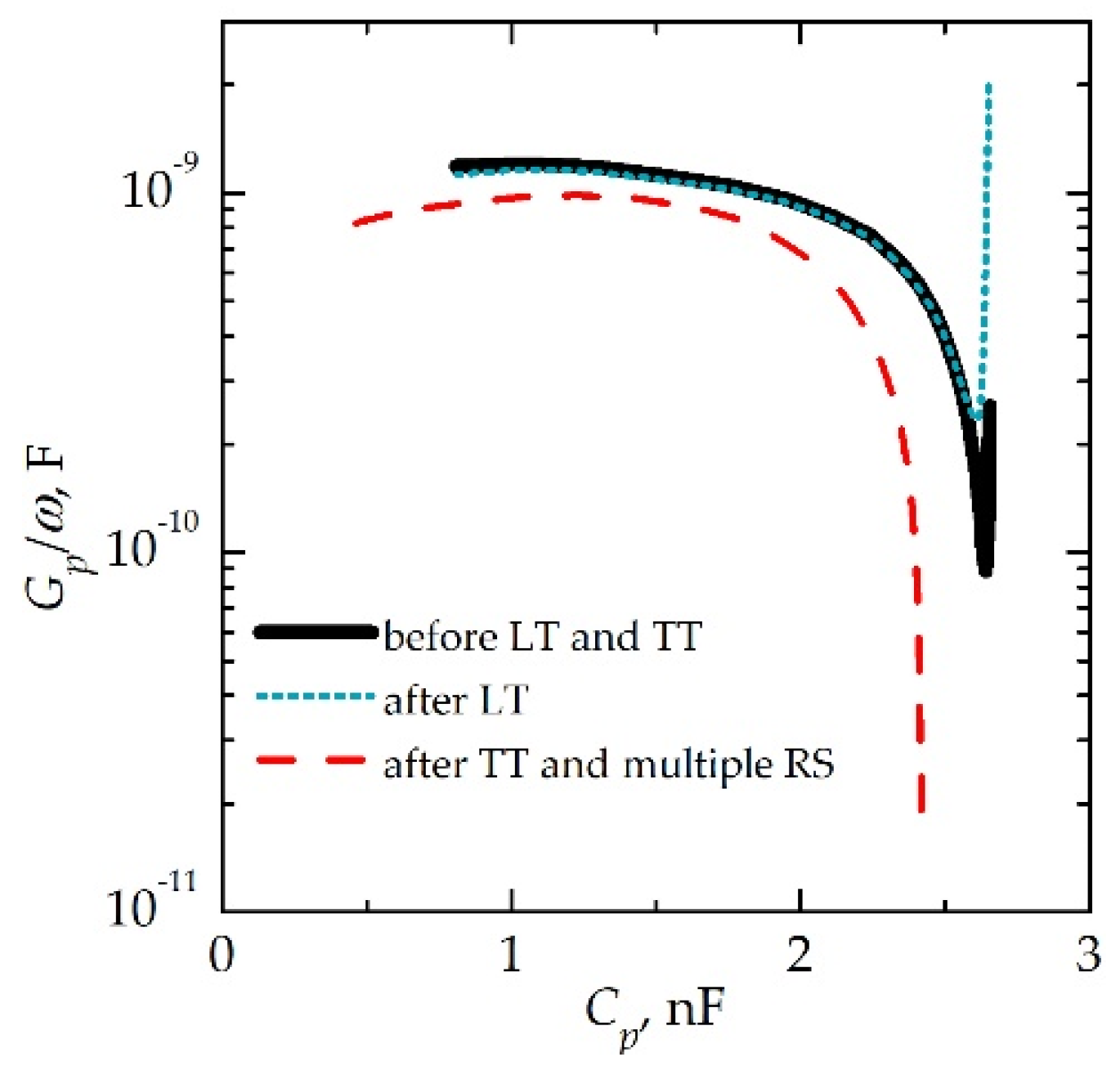
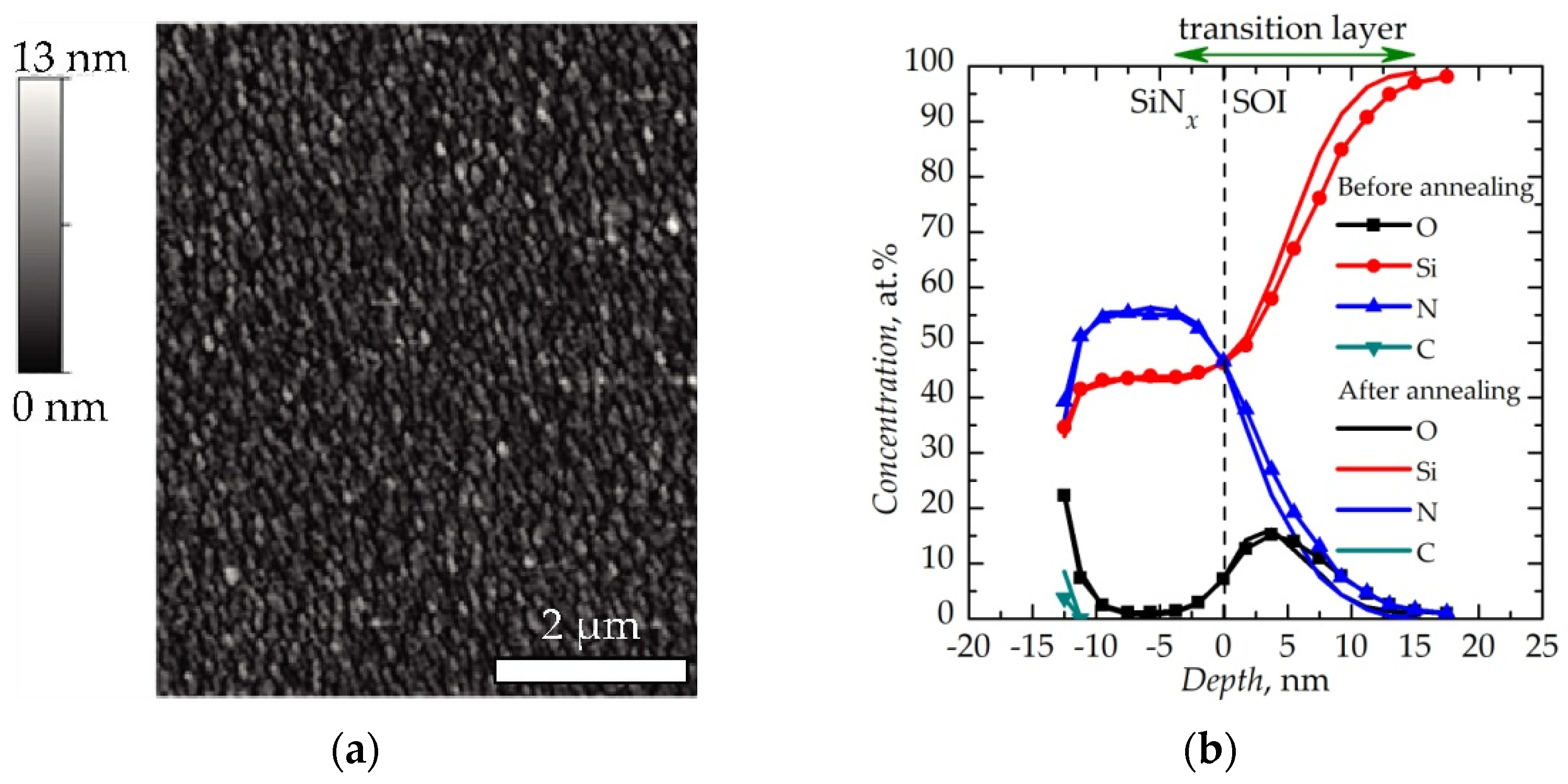
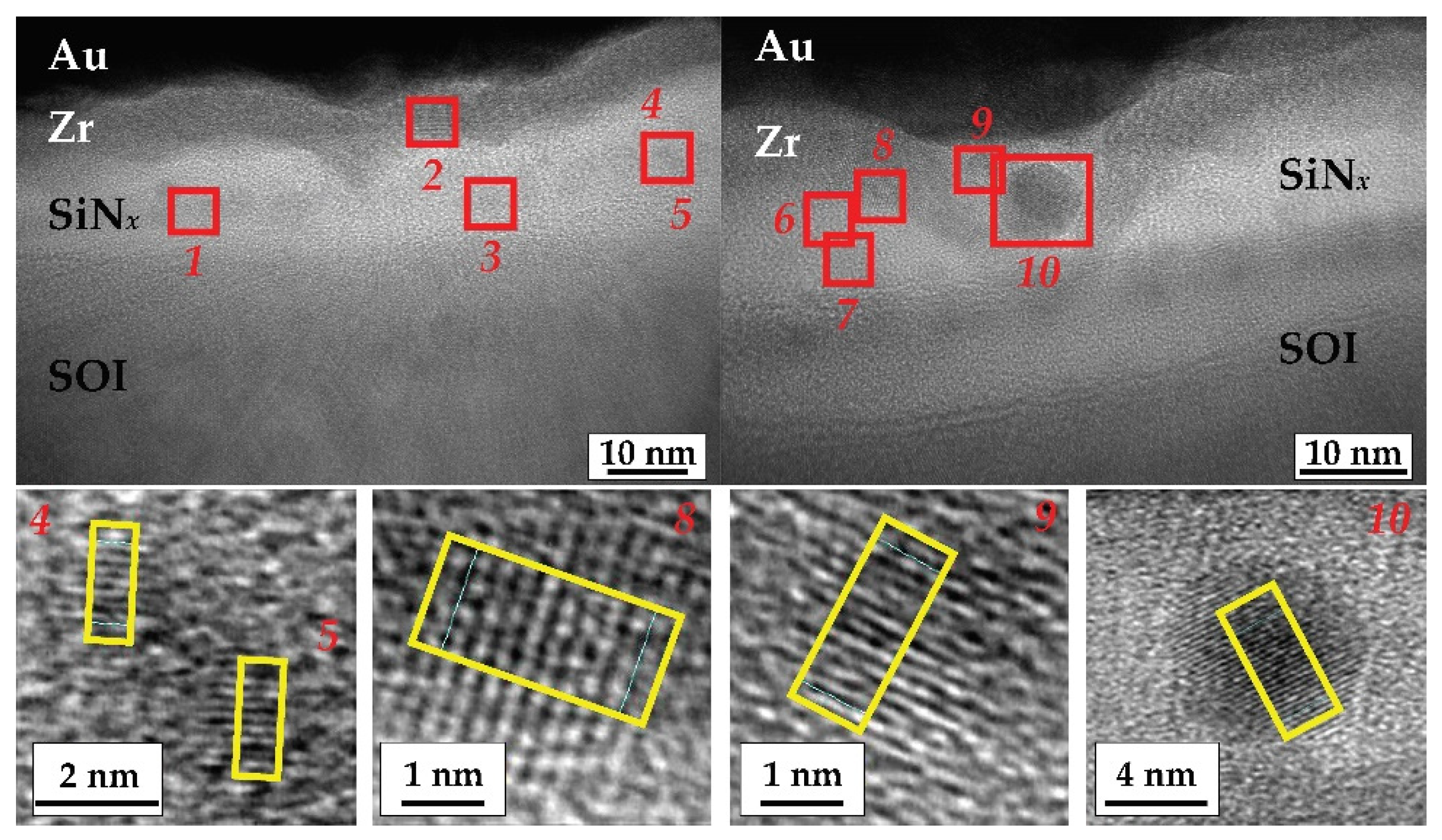
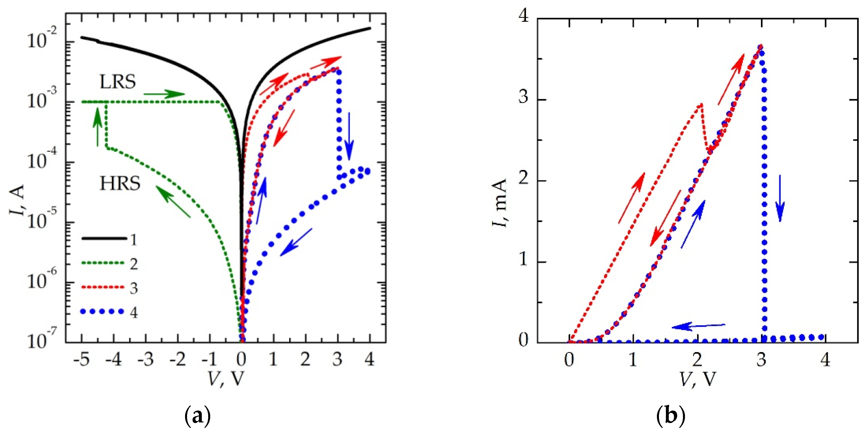
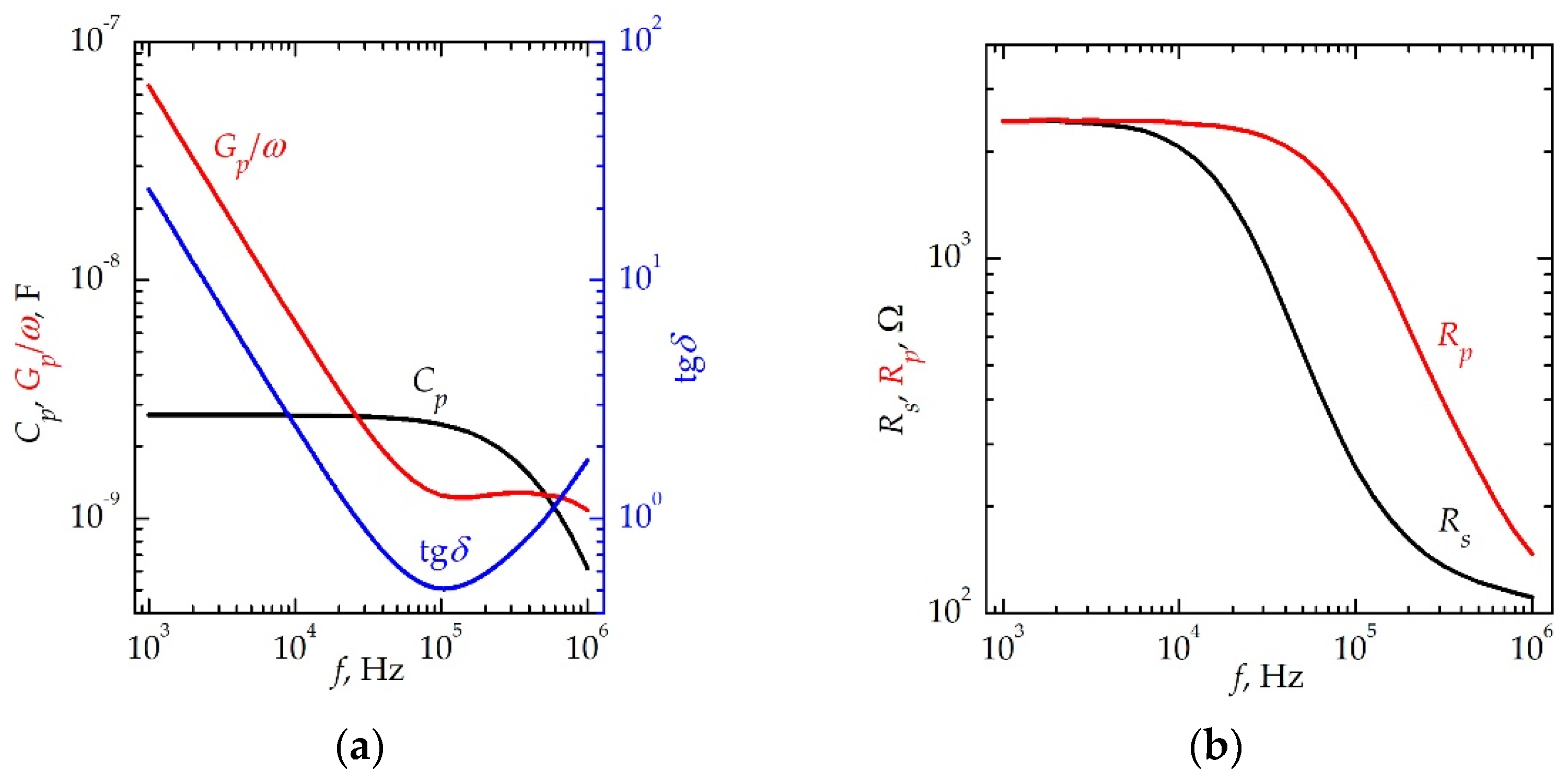
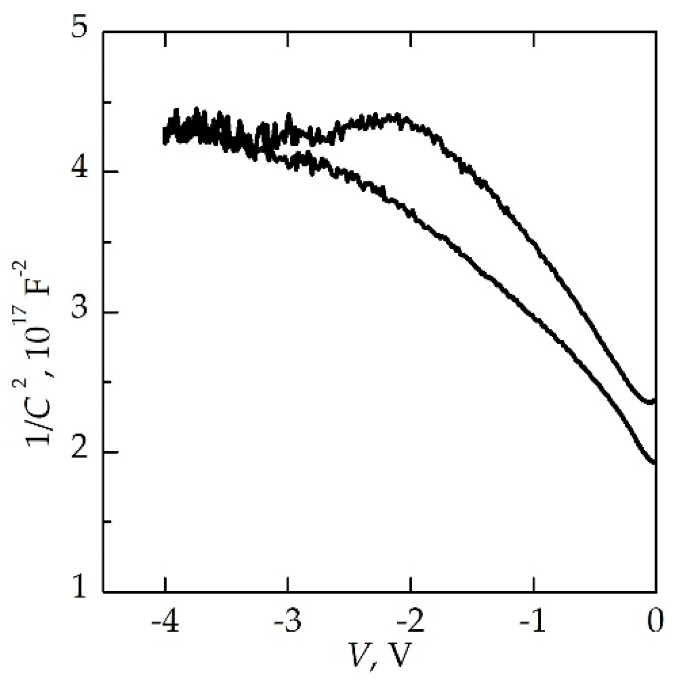
3.1. SiOx-Based Memristive Structures on SOI Substrates
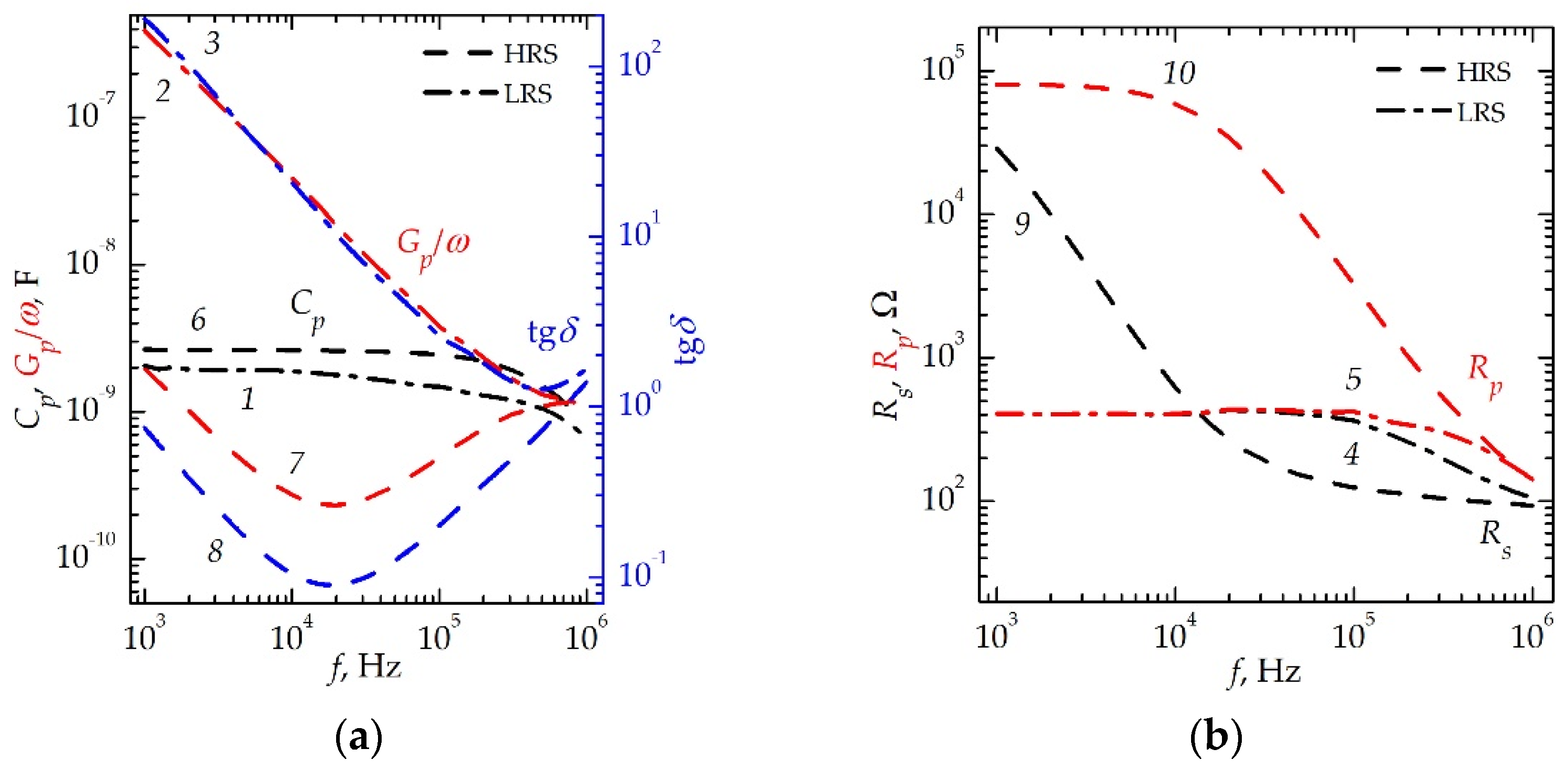
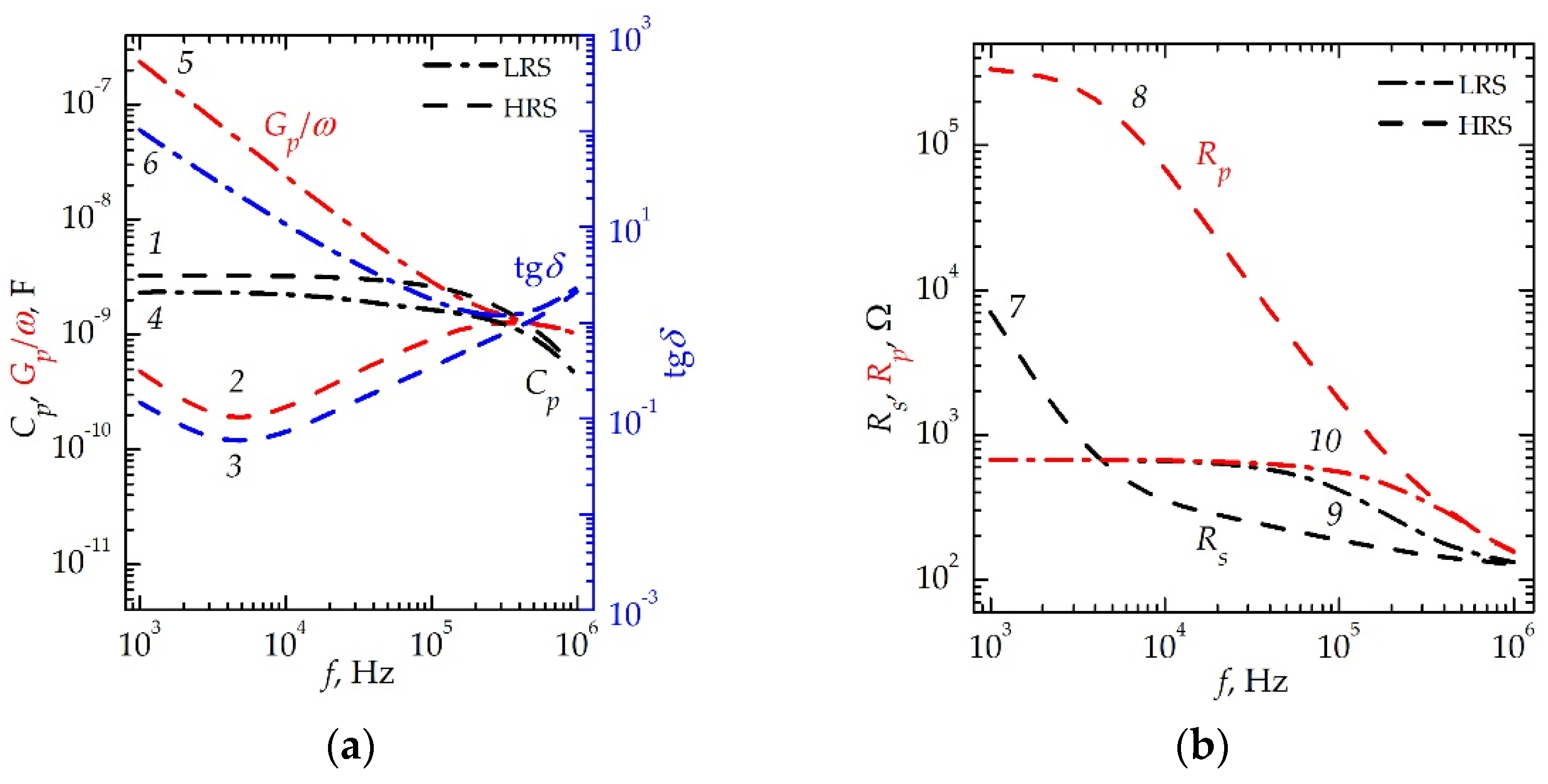
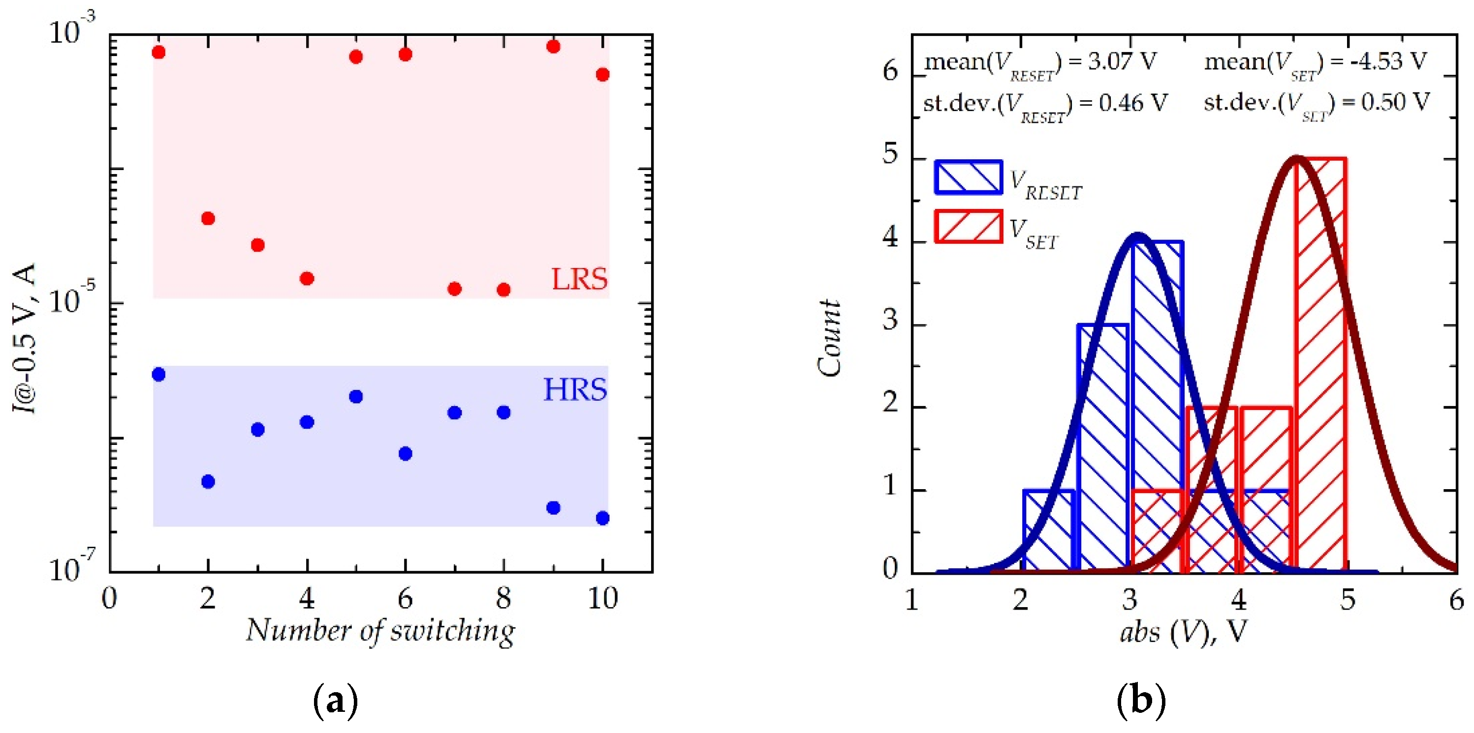
3.2. SiNx-Based Memristive Structures on SOI Substrates
4. Conclusions
Author Contributions
Funding
Data Availability Statement
Conflicts of Interest
References
- Zhang, W.; Gao, B.; Tang, J.; Li, X.; Wu, W.; Qian, H.; Wu, H. Analog-type resistive switching devices for neuromorphic computing. Phys. Status Solidi RRL 2019, 13, 1900204. [Google Scholar] [CrossRef]
- Wang, Z.; Joshi, S.; Savel’ev, S.E.; Jiang, H.; Midya, R.; Lin, P.; Hu, M.; Ge, N.; Strachan, J.P.; Li, Z.; et al. Memristors with diffusive dynamics as synaptic emulators for neuromorphic computing. Nat. Mater. 2017, 16, 101–108. [Google Scholar] [CrossRef] [PubMed] [Green Version]
- Slipko, V.A.; Pershin, Y.V. Metastable memristive lines for signal transmission and information processing applications. Phys. Rev. E 2017, 95, 042213. [Google Scholar] [CrossRef] [Green Version]
- Wang, Z.; Joshi, S.; Savel’ev, S.; Song, W.; Midya, R.; Li, Y.; Rao, M.; Yan, P.; Asapu, S.; Zhuo, Y.; et al. Fully memristive neural networks for pattern classification with unsupervised learning. Nat. Electron. 2018, 1, 137–145. [Google Scholar] [CrossRef]
- Pershin, Y.V.; Slipko, V.A. Dynamical attractors of memristors and their networks. Europhys. Lett. 2019, 125, 20002. [Google Scholar] [CrossRef] [Green Version]
- Pershin, Y.V. A demonstration of implication logic based on volatile (diffusive) memristors. IEEE Trans. Circuits Syst. II Express Briefs 2019, 66, 1033–1037. [Google Scholar] [CrossRef]
- Mehonic, A.; Sebastian, A.; Rajendran, B.; Simeone, O.; Vasilaki, E.; Kenyon, A.J. Memristors—From in-memory computing, deep learning acceleration, and spiking neural networks to the future of neuromorphic and bio-inspired computing. Adv. Intell. Syst. 2020, 2, 2000085. [Google Scholar] [CrossRef]
- Serb, A.; Corna, A.; George, R.; Khiat, A.; Rocchi, F.; Reato, M.; Maschietto, M.; Mayr, C.; Indiveri, G.; Vassanelli, S.; et al. Memristive synapses connect brain and silicon spiking neurons. Sci. Rep. 2020, 10, 2590. [Google Scholar] [CrossRef]
- Demin, V.A.; Nekhaev, D.V.; Surazhevsky, I.A.; Nikiruy, K.E.; Emelyanov, A.V.; Nikolaev, S.N.; Rylkov, V.V.; Kovalchuk, M.V. Necessary conditions for STDP-based pattern recognition learning in a memristive spiking neural network. Neural Netw. 2021, 134, 64–75. [Google Scholar] [CrossRef]
- Johnson, B.A.; Brahim, K.; Balanov, A.G.; Savel’ev, S.; Borisov, P. Transition from noise-induced to self-sustained current spiking generated by a NbOx thin film threshold switch. Appl. Phys. Lett. 2021, 118, 023502. [Google Scholar] [CrossRef]
- Ushakov, Y.; Akther, A.; Borisov, P.; Pattnaik, D.; Savel’ev, S.; Balanov, A.G. Deterministic mechanisms of spiking in diffusive memristors. Chaos Solitons Fractals 2021, 149, 110997. [Google Scholar] [CrossRef]
- Du, N.; Zhao, X.; Chen, Z.; Choubey, B.; Di Ventra, M.; Skorupa, I.; Bürger, D.; Schmidt, H. Synaptic plasticity in memristive artificial synapses and their robustness against noisy inputs. Front. Neurosci. 2021, 15, 696. [Google Scholar] [CrossRef] [PubMed]
- Mikhaylov, A.; Belov, A.; Korolev, D.; Antonov, I.; Kotomina, V.; Kotina, A.; Gryaznov, E.; Sharapov, A.; Koryazhkina, M.; Kryukov, R.; et al. Multilayer metal-oxide memristive device with stabilized resistive switching. Adv. Mater. Technol. 2020, 5, 1900607. [Google Scholar] [CrossRef]
- Nikiruy, K.E.; Iliasov, A.I.; Emelyanov, A.V.; Sitnikov, A.V.; Rylkov, V.V.; Demin, V.A. Memristors based on nanoscale layers LiNbO3 and (Co40Fe40B20)x(LiNbO3)100−x. Phys. Solid State 2020, 62, 1732–1735. [Google Scholar] [CrossRef]
- Matsukatova, A.N.; Emelyanov, A.V.; Minnekhanov, A.A.; Sakharutov, D.A.; Vdovichenko, A.Y.; Kamyshinskii, R.A.; Demin, V.A.; Rylkov, V.V.; Forsh, P.A.; Chvalun, S.N.; et al. Memristors based on poly(p-xylylene) with embedded silver nanoparticles. Tech. Phys. Lett. 2020, 46, 73–76. [Google Scholar] [CrossRef]
- Sun, K.; Chen, J.; Yan, X. The future of memristors: Materials engineering and neural networks. Adv. Funct. Mater. 2021, 31, 2006773. [Google Scholar] [CrossRef]
- La Torre, C.; Fleck, K.; Starschich, S.; Linn, E.; Waser, R.; Menzel, S. Dependence of the SET switching variability on the initial state in HfOx-based ReRAM. Phys. Status Solidi A 2016, 213, 316–319. [Google Scholar] [CrossRef]
- Ungureanu, M.; Zazpe, R.; Golmar, F.; Stoliar, P.; Llopis, R.; Casanova, F.; Hueso, L.E. A light-controlled resistive switching memory. Adv. Mater. 2012, 24, 2496–2500. [Google Scholar] [CrossRef]
- Patterson, G.A.; Fierens, P.I.; Grosz, D.F. On the beneficial role of noise in resistive switching. Appl. Phys. Lett. 2013, 103, 074102. [Google Scholar] [CrossRef] [Green Version]
- Mikhaylov, A.N.; Guseinov, D.V.; Belov, A.I.; Korolev, D.S.; Shishmakova, V.A.; Koryazhkina, M.N.; Filatov, D.O.; Gorshkov, O.N.; Maldonado, D.; Alonso, F.J.; et al. Stochastic resonance in a metal-oxide memristive device. Chaos Solitons Fractals 2021, 144, 110723. [Google Scholar] [CrossRef]
- Ntinas, V.; Rubio, A.; Sirakoulis, G.C.; Aguilera, E.S.; Pedro, M.; Crespo-Yepes, A.; Martin-Martinez, J.; Rodriguez, R.; Nafria, M. Power-efficient noise-induced reduction of ReRAM cell’s temporal variability effects. IEEE Trans. Circuits Syst. II Express Briefs 2021, 68, 1378–1382. [Google Scholar] [CrossRef]
- Ielmini, D.; Nardi, F.; Cagli, C. Resistance-dependent amplitude of random telegraph-signal noise in resistive switching memories. Appl. Phys. Lett. 2010, 96, 053503. [Google Scholar] [CrossRef]
- Marchewka, A.; Waser, R.; Menzel, S. Physical simulation of dynamic resistive switching in metal oxides using a Schottky contact barrier model. In Proceedings of the International Conference on Simulation of Semiconductor Processes and Devices (SISPAD), Washington, DC, USA, 9–11 September 2015; IEEE: New York, NY, USA, 2015; pp. 297–300. [Google Scholar] [CrossRef]
- Strukov, D.B.; Alibart, F.; Stanley Williams, R. Thermophoresis/diffusion as a plausible mechanism for unipolar resistive switching in metal-oxide-metal memristors. Appl. Phys. A 2012, 107, 509–518. [Google Scholar] [CrossRef]
- Guarcello, C.; Valenti, D.; Spagnolo, B. Phase dynamics in graphene-based Josephson junctions in the presence of thermal and correlated fluctuations. Phys. Rev. B 2015, 92, 174519. [Google Scholar] [CrossRef] [Green Version]
- Carollo, A.; Spagnolo, B.; Valenti, D. Uhlmann curvature in dissipative phase transitions. Sci. Rep. 2018, 8, 9852. [Google Scholar] [CrossRef] [PubMed] [Green Version]
- Jiang, H.; Han, L.; Lin, P.; Wang, Z.; Jang, M.H.; Wu, Q.; Barnell, M.; Yang, J.J.; Xin, H.L.; Xia, Q. Sub-10 nm Ta channel responsible for superior performance of a HfO2 memristor. Sci. Rep. 2016, 6, 28525. [Google Scholar] [CrossRef] [PubMed] [Green Version]
- Lu, K.; Li, Y.; He, W.F.; Chen, J.; Zhou, Y.X.; Duan, N.; Jin, M.M.; Gu, W.; Xue, K.H.; Sun, H.J.; et al. Diverse spike-timing-dependent plasticity based on multilevel HfOx memristor for neuromorphic computing. Appl. Phys. A 2018, 124, 438. [Google Scholar] [CrossRef]
- Lian, X.; Wang, M.; Rao, M.; Yan, P.; Yang, J.J.; Miao, F. Characteristics and transport mechanisms of triple switching regimes of TaOx memristor. Appl. Phys. Lett. 2017, 110, 173504. [Google Scholar] [CrossRef]
- Choi, S.; Jang, S.; Moon, J.H.; Kim, J.C.; Jeong, H.Y.; Jang, P.; Lee, K.J.; Wang, G. A self-rectifying TaOy/nanoporous TaOx memristor synaptic array for learning and energy-efficient neuromorphic systems. NPG Asia Mater. 2018, 10, 1097–1106. [Google Scholar] [CrossRef] [Green Version]
- Abbas, Y.; Han, I.S.; Sokolov, A.S.; Jeon, Y.R.; Choi, C. Rapid thermal annealing on the atomic layer-deposited zirconia thin film to enhance resistive switching characteristics. J. Mater. Sci. Mater. Electron. 2020, 31, 903–909. [Google Scholar] [CrossRef]
- Upadhyay, N.K.; Sun, W.; Lin, P.; Joshi, S.; Midya, R.; Zhang, X.; Wang, Z.; Jiang, H.; Yoon, J.H.; Rao, M.; et al. A memristor with low switching current and voltage for 1S1R integration and array operation. Adv. Electron. Mater. 2020, 6, 1901411. [Google Scholar] [CrossRef]
- Gambuzza, L.V.; Samardzic, N.; Dautovic, S.; Xibilia, M.G.; Graziani, S.; Fortuna, L.; Stojanovic, G.; Frasca, M. A data driven model of TiO2 printed memristors. In Proceedings of the 8th International Conference on Electrical and Electronics Engineering (ELECO), Bursa, Turkey, 28–30 November 2013; pp. 1–4. [Google Scholar] [CrossRef]
- Kim, M.; Yoo, K.; Jeon, S.P.; Park, S.K.; Kim, Y.H. The effect of multi-layer stacking sequence of TiOx active layers on the resistive-switching characteristics of memristor devices. Micromachines 2020, 11, 154. [Google Scholar] [CrossRef] [PubMed] [Green Version]
- Cvejin, K.; Mojić, B.; Samardžić, N.; Srdić, V.V.; Stojanović, G.M. Dielectric studies of barium bismuth titanate as a material for application in temperature sensors. J. Mater. Sci. Mater. Electron. 2013, 24, 1243–1249. [Google Scholar] [CrossRef]
- Vasileiadis, N.; Karakolis, P.; Mandylas, P.; Ioannou-Sougleridis, V.; Normand, P.; Perego, M.; Komninou, P.; Ntinas, V.; Fyrigos, I.A.; Karafyllidis, I.; et al. Understanding the role of defects in silicon nitride-based resistive switching memories through oxygen doping. IEEE Trans. Nanotechnol. 2021, 20, 356–364. [Google Scholar] [CrossRef]
- Vasileiadis, N.; Ntinas, V.; Fyrigos, I.A.; Karamani, R.E.; Ioannou-Sougleridis, V.; Normand, P.; Karafyllidis, I.; Sirakoulis, G.C.; Dimitrakis, P. A new 1P1R image sensor with in-memory computing properties based on silicon nitride devices. In Proceedings of the IEEE International Symposium on Circuits and Systems (ISCAS), Daegu, Korea, 22–28 May 2021; IEEE: New York, NY, USA, 2021; pp. 1–5. [Google Scholar] [CrossRef]
- Ambrosi, E.; Bricalli, A.; Laudato, M.; Ielmini, D. Impact of oxide and electrode materials on the switching characteristics of oxide ReRAM devices. Faraday Discuss. 2019, 213, 87–98. [Google Scholar] [CrossRef] [Green Version]
- Yen, T.-J.; Chin, A.; Gritsenko, V. Improved device distribution in high-performance SiNx Resistive Random Access Memory via Arsenic ion implantation. Nanomaterials 2021, 11, 1401. [Google Scholar] [CrossRef]
- Duchamp, M.; Migunov, V.; Tavabi, A.H.; Mehonic, A.; Buckwell, M.; Munde, M.; Kenyon, A.J.; Dunin-Borkowski, R.E. In situ transmission electron microscopy of resistive switching in thin silicon oxide layers. Resolut. Discov. 2016, 1, 27–33. [Google Scholar] [CrossRef] [Green Version]
- Jiang, X.; Ma, Z.; Yang, H.; Yu, J.; Wang, W.; Zhang, W.; Li, W.; Xu, J.; Xu, L.; Chen, K.; et al. Nanocrystalline Si pathway induced unipolar resistive switching behavior from annealed Si-rich SiNx/SiNy multilayers. J. Appl. Phys. 2014, 116, 123705. [Google Scholar] [CrossRef]
- Islamov, D.R.; Gritsenko, V.A.; Chin, A. Charge transport in thin hafnium and zirconium oxide films. Optoelectron. Instrument. Proc. 2017, 53, 184–189. [Google Scholar] [CrossRef]
- Gismatulin, A.A.; Orlov, O.M.; Gritsenko, V.A.; Kruchinin, V.N.; Mizginov, D.S.; Krasnikov, G.Y. Charge transport mechanism in the metal–nitride–oxide–silicon forming-free memristor structure. Appl. Phys. Lett. 2020, 116, 203502. [Google Scholar] [CrossRef]
- Bishop, M.D.; Wong, H.S.P.; Mitra, S.; Shulaker, M.M. Monolithic 3-D integration. IEEE Micro 2019, 39, 16–27. [Google Scholar] [CrossRef]
- Saylan, S.; Aldosari, H.M.; Humood, K.; Abi Jaoude, M.; Ravaux, F.; Mohammad, B. Effects of top electrode material in hafnium-oxide-based memristive systems on highly-doped Si. Sci. Rep. 2020, 10, 19541. [Google Scholar] [CrossRef] [PubMed]
- Popov, V.P.; Antonova, A.I.; Frantsuzov, A.A.; Safronov, L.N.; Feofanov, G.N.; Naumova, O.V.; Kilanov, D.V. Properties of silicon-on-insulator structures and devices. Semiconductors 2001, 35, 1030–1037. [Google Scholar] [CrossRef]
- Hoessbacher, C.; Fedoryshyn, Y.; Emboras, A.; Melikyan, A.; Kohl, M.; Hillerkuss, D.; Hafner, C.; Leuthold, J. The plasmonic memristor: A latching optical switch. Optica 2014, 1, 198–202. [Google Scholar] [CrossRef]
- Puppo, F.; Doucey, M.A.; Di Ventra, M.; De Micheli, G.; Carrara, S. Memristor-based devices for sensing. In Proceedings of the IEEE International Symposium on Circuits and Systems (ISCAS), Melbourne, VIC, Australia, 1–5 June 2014; IEEE: New York, NY, USA, 2014; pp. 2257–2260. [Google Scholar] [CrossRef] [Green Version]
- Li, C.; Han, L.; Jiang, H.; Jang, M.-H.; Lin, P.; Wu, Q.; Barnell, M.; Yang, J.J.; Xin, H.L.; Xia, Q. Three-dimensional crossbar arrays of self-rectifying Si/SiO2/Si memristors. Nat. Commun. 2017, 8, 15666. [Google Scholar] [CrossRef]
- Pragnya, P.; Pinkowitz, A.; Hull, R.; Gall, D. Electrochemical memristive devices based on submonolayer metal deposition. APL Mater. 2019, 7, 101121. [Google Scholar] [CrossRef]
- Baltakesmez, A. Improved barrier parameters and working stability of Au/p-GO/n-lnP/Au–Ge Schottky barrier diode with GO interlayer showing resistive switching effect. Vacuum 2019, 168, 108825. [Google Scholar] [CrossRef]
- Skorobogatov, S. Local heating attacks on flash memory devices. In Proceedings of the IEEE International Workshop on Hardware-Oriented Security and Trust (HOST), San Francisco, CA, USA, 27 July 2009; IEEE: New York, NY, USA, 2009; pp. 1–6. [Google Scholar] [CrossRef] [Green Version]
- Kärkkänen, I.; Shkabko, A.; Heikkilä, M.; Vehkamäki, M.; Niinistö, J.; Aslam, N.; Meuffels, P.; Ritala, M.; Leskelä, M.; Waser, R.; et al. Impedance spectroscopy study of the unipolar and bipolar resistive switching states of atomic layer deposited polycrystalline ZrO2 thin films. Phys. Status Solidi A 2015, 212, 751–766. [Google Scholar] [CrossRef]
- Epshtein, S.L. Measuring of Capacitor Characteristics; Energiya: Moscow, Russia, 1965; 236p. (In Russian) [Google Scholar]
- Oreshkin, P.T. Physics of Semiconductors and Dielectrics; Vysshaya Shkola: Moscow, Russia, 1977; 448p. (In Russian) [Google Scholar]
- Ovsyuk, V.N. Electronic Processes in Semiconductors with Space-Charge Regions; Nauka: Novosibirsk, Russia, 1984; 254p. (In Russian) [Google Scholar]
- Antipov, A.; Arakelian, S.; Vartanyan, T.; Gerke, M.; Istratov, A.; Kutrovskaya, S.; Kucherik, A.; Osipov, A. Optical properties of multilayer bimetallic films obtained by laser deposition of colloidal particles. Opt. Spectrosc. 2016, 121, 765–768. [Google Scholar] [CrossRef]
- Hofmann, S. Auger- and X-ray Photoelectron Spectroscopy in Materials Science; Springer: Berlin/Heidelberg, Germany, 2013; 528p. [Google Scholar] [CrossRef]
- Wang, T.Y.; Meng, J.L.; Li, Q.X.; Chen, L.; Zhu, H.; Sun, Q.Q.; Ding, S.J.; Zhang, D.W. Forming-free flexible memristor with multilevel storage for neuromorphic computing by full PVD technique. J. Mater. Sci. Technol. 2021, 60, 21–26. [Google Scholar] [CrossRef]
- Gorshkov, O.N.; Mikhaylov, A.N.; Kasatkin, A.P.; Tikhov, S.V.; Filatov, D.O.; Pavlov, D.A.; Belov, A.I.; Koryazhkina, M.N.; Bobrov, A.I.; Malekhonova, N.V.; et al. Resistive switching in the Au/Zr/ZrO2-Y2O3/TiN/Ti memristive devices deposited by magnetron sputtering. J. Phys. Conf. Ser. 2016, 741, 012174. [Google Scholar] [CrossRef]
- Gurtov, V.A. Solid State Electronics; Tekhnosfera: Moscow, Russia, 2008; 512p. (In Russian) [Google Scholar]
- Ismail, M.; Kim, S. Negative differential resistance effect and dual bipolar resistive switching properties in a transparent Ce-based devices with opposite forming polarity. Appl. Surf. Sci. 2020, 530, 147284. [Google Scholar] [CrossRef]
- Kumar, N.; Chand, S. Effects of temperature, bias and frequency on the dielectric properties and electrical conductivity of Ni/SiO2/p-Si/Al MIS Schottky diodes. J. Alloys Compd. 2020, 817, 153294. [Google Scholar] [CrossRef]
- Hasegawa, H.; Sawada, T. On the electrical properties of compound semiconductor interfaces in metal/insulator/semiconductor structures and the possible origin of interface states. Thin Solid Films 1983, 103, 119–140. [Google Scholar] [CrossRef]
- Chaabouni, F.; Abaab, M.; Rezig, B. Characterization of n-ZnO/p-Si films grown by magnetron sputtering. Superlattices Microstruct. 2006, 39, 171–178. [Google Scholar] [CrossRef]
- Hu, C. Modern Semiconductor Devices for Integrated Circuits; Pearson: London, UK, 2010; p. 351. [Google Scholar]
- Wang, L.G.; Zhang, W.; Chen, Y.; Cao, Y.Q.; Li, A.D.; Wu, D. Synaptic plasticity and learning behaviors mimicked in single inorganic synapses of Pt/HfOx/ZnOx/TiN memristive system. Nanoscale Res. Lett. 2017, 12, 65. [Google Scholar] [CrossRef] [PubMed] [Green Version]
- Krishnaprasad, A.; Choudhary, N.; Das, S.; Dev, D.; Kalita, H.; Chung, H.S.; Aina, O.; Jung, Y.; Roy, T. Electronic synapses with near-linear weight update using MoS2/graphene memristors. Appl. Phys. Lett. 2019, 115, 103104. [Google Scholar] [CrossRef]
- Nasyrov, K.A.; Shaĭmeev, S.S.; Gritsenko, V.A.; Han, J.H.; Kim, C.W.; Lee, J.-W. Electron and hole injection in metal-oxide-nitride-oxide-silicon structures. J. Exp. Theor. Phys. 2006, 102, 810–820. [Google Scholar] [CrossRef]
- Gismatulin, A.A.; Gritsenko, V.A.; Yen, T.-J.; Chin, A. Charge transport mechanism in SiNx-based memristor. Appl. Phys. Lett. 2019, 115, 253502. [Google Scholar] [CrossRef]
- Mikhaylov, A.N.; Belov, A.I.; Guseinov, D.V.; Korolev, D.S.; Antonov, I.N.; Efimovykh, D.V.; Tikhov, S.V.; Kasatkin, A.P.; Gorshkov, O.N.; Tetelbaum, D.I.; et al. Bipolar resistive switching and charge transport in silicon oxide memristor. Mater. Sci. Eng. B 2015, 194, 48–54. [Google Scholar] [CrossRef]


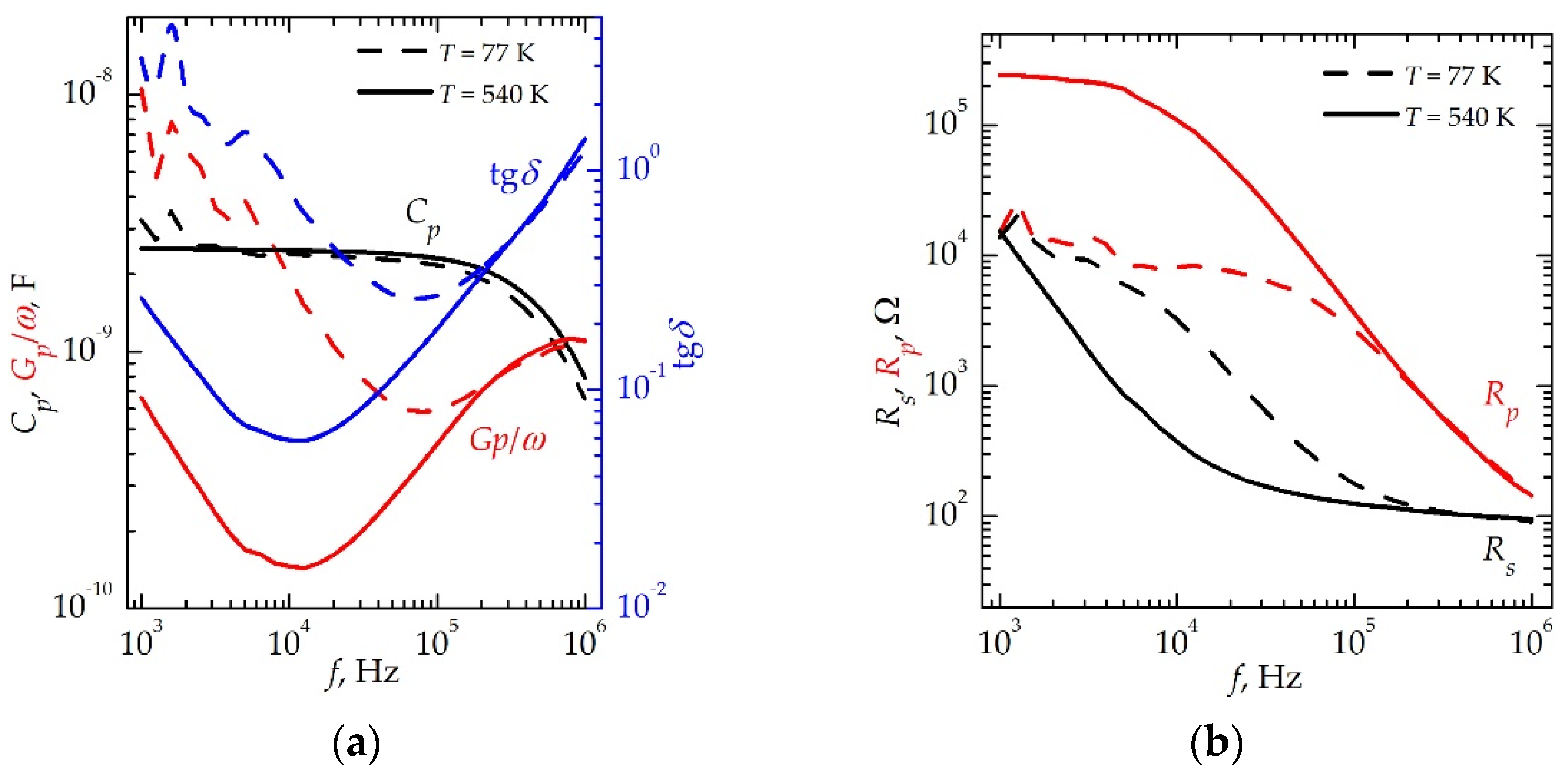
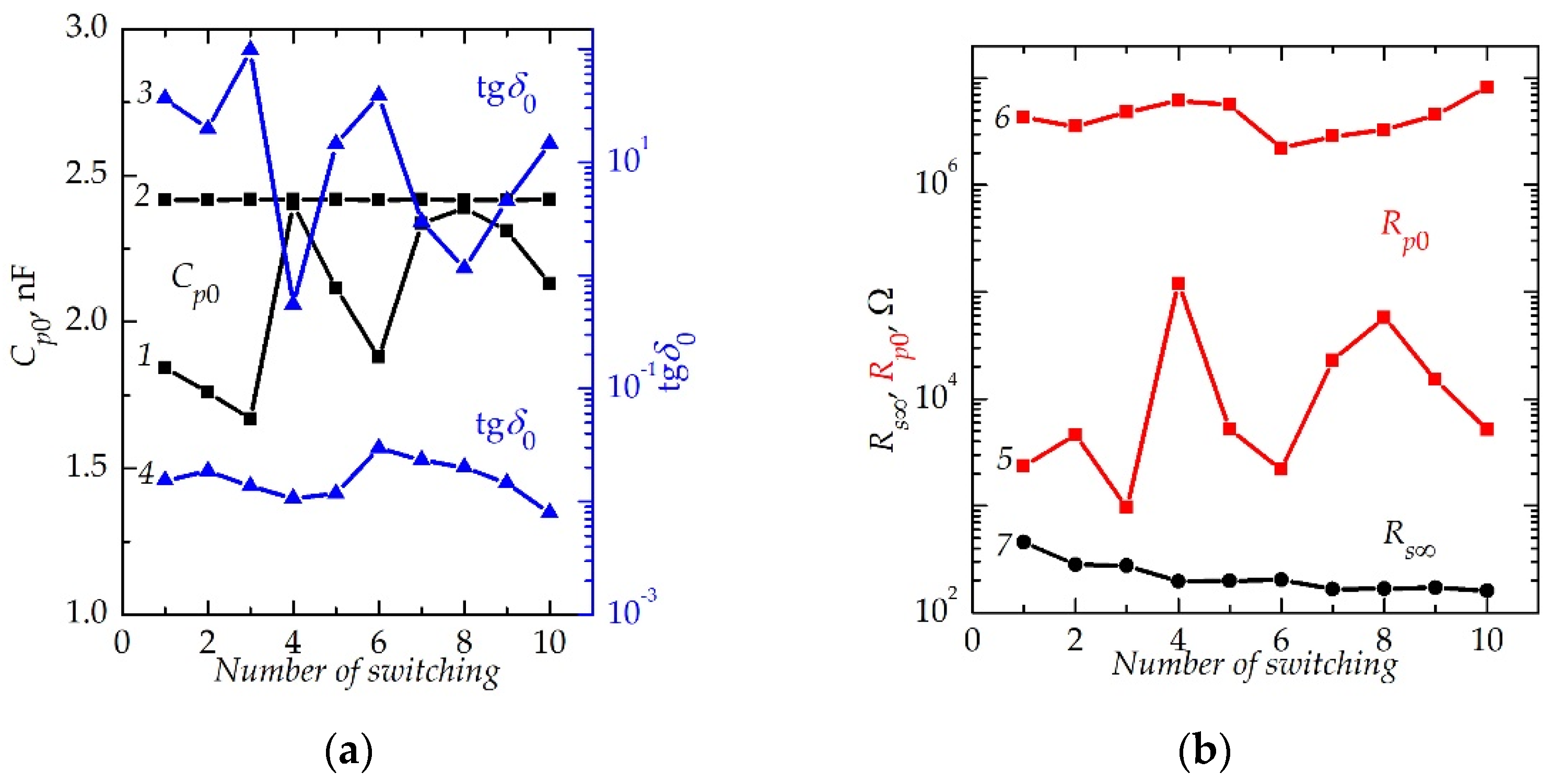
| Treatment | Resistive State | Cp0, nF | Cp∞, nF | Gp0/ω, nF | Gp∞/ω, nF | tgδ0 | tgδ∞ | Rp0, Ω | Rp∞, Ω | Rs0, Ω | Rs∞, Ω |
|---|---|---|---|---|---|---|---|---|---|---|---|
| Before LT and TT | IS | 2.05 | 1.60 | 334 | 3.68 | 163 | 2.30 | 476 | 433 | 476 | 364 |
| HRS | 2.65 | 2.46 | 0.26 | 0.47 | 0.10 | 0.19 | 621,296 | 3400 | 5732 | 119 | |
| After LT | LRS | 2.06 | 1.49 | 390 | 3.78 | 189 | 2.54 | 409 | 422 | 409 | 365 |
| HRS | 2.65 | 2.45 | 1.98 | 0.49 | 0.75 | 0.20 | 80,309 | 3253 | 28,806 | 125 | |
| During TT | HRS at 77 K | 3.24 | 2.17 | 11 | 0.59 | 3.24 | 0.27 | 15,124 | 2701 | 13,812 | 179 |
| HRS at 540 K | 2.52 | 2.31 | 0.66 | 0.44 | 0.26 | 0.19 | 241,206 | 3637 | 15,457 | 126 | |
| After multiple RS | HRS | 2.42 | 2.02 | 0.02 | 0.66 | 0.01 | 0.33 | 8,259,960 | 2396 | 525 | 234 |
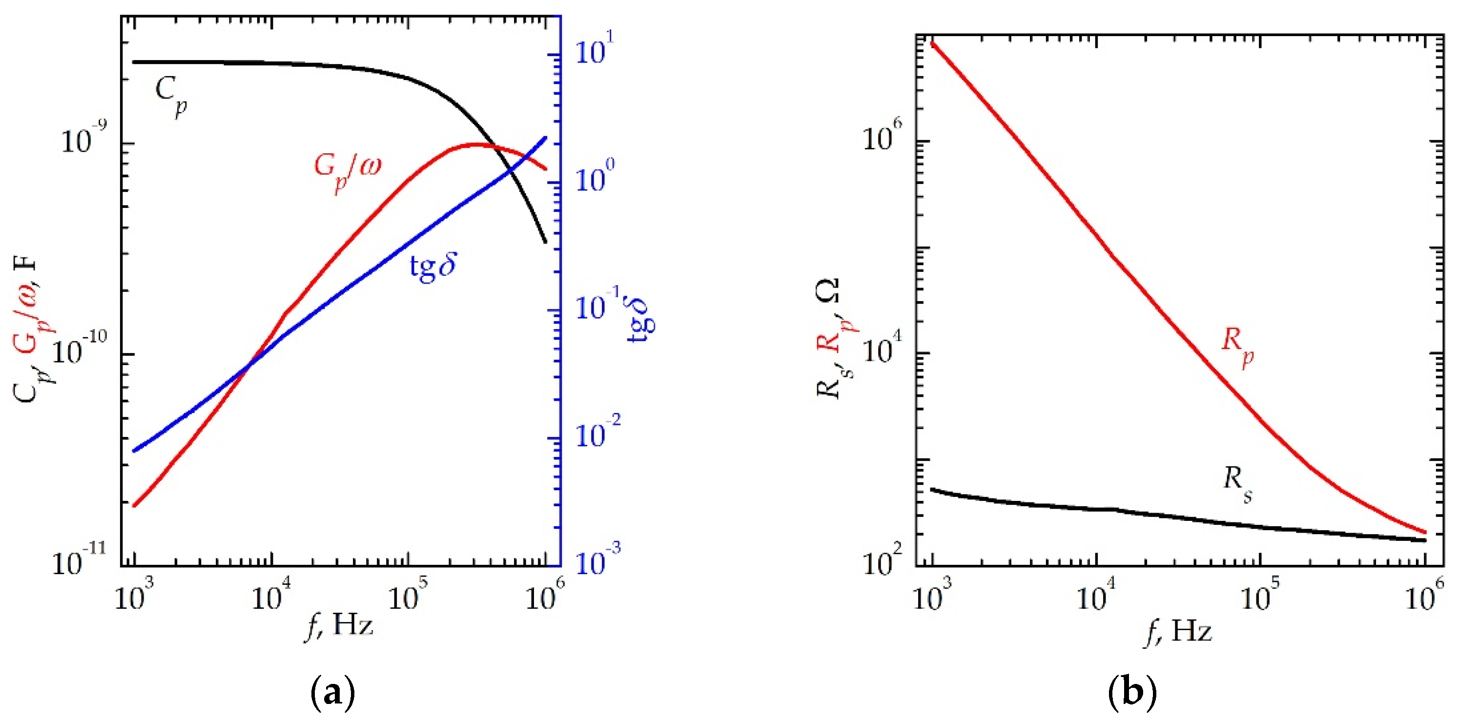
| Treatment | Resistive State | Cp0, nF | Cp∞, nF | Gp0/ω, nF | Gp∞/ω, nF | tgδ0 | tgδ∞ | Rp0, Ω | Rp∞, Ω | Rs0, Ω | Rs∞, Ω |
|---|---|---|---|---|---|---|---|---|---|---|---|
| Before LT | IS | 2.71 | 2.48 | 65 | 1.25 | 24 | 0.50 | 2436 | 1276 | 2432 | 258 |
| After LT | LRS | 2.30 | 1.64 | 236 | 2.86 | 102 | 1.74 | 675 | 558 | 675 | 419 |
| HRS | 3.26 | 2.61 | 0.48 | 0.90 | 0.15 | 0.35 | 334,200 | 1764 | 6992 | 188 |
Publisher’s Note: MDPI stays neutral with regard to jurisdictional claims in published maps and institutional affiliations. |
© 2022 by the authors. Licensee MDPI, Basel, Switzerland. This article is an open access article distributed under the terms and conditions of the Creative Commons Attribution (CC BY) license (https://creativecommons.org/licenses/by/4.0/).
Share and Cite
Koryazhkina, M.N.; Filatov, D.O.; Tikhov, S.V.; Belov, A.I.; Korolev, D.S.; Kruglov, A.V.; Kryukov, R.N.; Zubkov, S.Y.; Vorontsov, V.A.; Pavlov, D.A.; et al. Silicon-Compatible Memristive Devices Tailored by Laser and Thermal Treatments. J. Low Power Electron. Appl. 2022, 12, 14. https://0-doi-org.brum.beds.ac.uk/10.3390/jlpea12010014
Koryazhkina MN, Filatov DO, Tikhov SV, Belov AI, Korolev DS, Kruglov AV, Kryukov RN, Zubkov SY, Vorontsov VA, Pavlov DA, et al. Silicon-Compatible Memristive Devices Tailored by Laser and Thermal Treatments. Journal of Low Power Electronics and Applications. 2022; 12(1):14. https://0-doi-org.brum.beds.ac.uk/10.3390/jlpea12010014
Chicago/Turabian StyleKoryazhkina, Maria N., Dmitry O. Filatov, Stanislav V. Tikhov, Alexey I. Belov, Dmitry S. Korolev, Alexander V. Kruglov, Ruslan N. Kryukov, Sergey Yu. Zubkov, Vladislav A. Vorontsov, Dmitry A. Pavlov, and et al. 2022. "Silicon-Compatible Memristive Devices Tailored by Laser and Thermal Treatments" Journal of Low Power Electronics and Applications 12, no. 1: 14. https://0-doi-org.brum.beds.ac.uk/10.3390/jlpea12010014