Article

A 0.18-ns Response Time Digital LDO Regulator with Adaptive PI Controller in 180-nm CMOS

Faculty of Information Technology, College of Microelectronics, Beijing University of Technology, Beijing 100124, China
*
Author to whom correspondence should be addressed.
These authors contributed equally to this work.
Submission received: 24 May 2021 / Revised: 21 June 2021 / Accepted: 7 July 2021 / Published: 13 July 2021
(This article belongs to the Special Issue Design of Mixed Analog/Digital Circuits)

Abstract

:
Digital low drop-out regulator (D-LDO) with fast settling time and superior transient response is gaining increasing attention to make up for the deficiency of analog LDO. However, as the traditional digital LDOs regulate the output voltage code at a rate of 1 bit per clock cycle, the transient response speed is limited. In this paper, a multi-bit conversion technique is proposed to improve the transient response speed. The multi-bit conversion technique is achieved by an error detector with adaptive regulation of proportion and integration parameters in the digital controller before pass devices. Besides, a voltage sensor and a time-to-digital converter are employed to convert the output voltage to digital codes. Implemented in a 180-nm CMOS process, the proposed D-LDO features under 36/33 mV of undershoot/overshoot at V OUT = 0.95 V as the load current steps up with 40 mA/1 ns on a 0.5 nF load capacitor. The simulated response time is 0.18-ns, the figure-of-merit of speed FOM1 is 0.65 ps and FOM2 achieves 0.068 pF.

1. Introduction

Digital low drop-out regulator (D-LDO), enjoying a wide range of applications in the Internet of Things (IoT) technology, has recently become one of the main topics of much research in the field of wireless communications. LDOs normally use power from the battery or the energy harvest. In such conditions, LDOs are desired to improve battery life and improve user experiences with immediate transition. In particular, the application of the IoT makes that the battery or the energy harvest provide supply voltage lower than ever. Hence, the stability is harder to control because the decrease of dynamic range and bandwidth of integrated circuits.
Conventional LDOs have been designed with analog circuits and employed an error amplifier and a driver amplifier to provide voltage regulation with negative feedback. They exhibit high efficiency, fast response time and high power supply rejection (PSR) [1,2,3]. However, it is difficult for analog LDOs to operating at low supply voltage, which has prompted the digital implementations of LDOs [4].
Comparing with analog LDOs, the digital low-dropout regulator (D-LDO) is more suitable for low-supply-voltage operation, and the input-voltage range of D-LDOs is unlimited without error amplifiers. In addition, D-LDO has better scalability and portability exploiting the benefit of digital-logic characteristics. Employing a large number of shift-register, conventional D-LDO has a slower transient response than the analog LDO [5]. Fast load regulation is important in digital circuits with rapidly changing supply current. In [6,7,8], D-LDOs with an improved triggered comparator have been proposed to improve the transient response, but the performances of the D-LDOs are limited by the analog-to-digital interface, i.e., the comparator. Ref. [9] has categorized all the existing LDO designs by their control methods. Itpresents the hybrid LDO is a good low-voltage solution with fast transient response and also certain power supply rejection. In [10], D-LDO with transient enhanced PI controller which forms control deviation according to the given value and the actual output value achieves fast transient settling by adjusting the gain of PI controller, and the load current variation can be improved as well. D-LDO in [11] boosts loop-gain dynamically during load transients by a load transient detector without compromising the stability of the D-LDO at steady-state operation, but there may be a deviation in the regulation because of the analog-to-digital converter (ADC).
In this paper, a D-LDO with fast settling time and low undershoot/overshoot is proposed. To improve the load transient response, a time-to-digital converter (TDC) based converter and a PI controller are adopted to achieve a multi-bit regulation. By combining the benefits of both analog and digital control loops with PI controller can be a good low-voltage solution with fast response. The settling time is reduced by five times to 26 ns. In addition, an error detector is proposed to adjust the coefficient of the PI controller adaptively and reduce undershoot/overshoot voltage to 36/33 mV with 40 mA/ns.
The remainder of this paper is organized as follows: In Section 2, the architecture of the D-LDO is proposed. Section 3 presents the details of the circuit implementation of the proposed structure. The simulation results, discussions, and comparisons are illustrated in Section 4. Finally, the conclusion of this paper is given in Section 5.

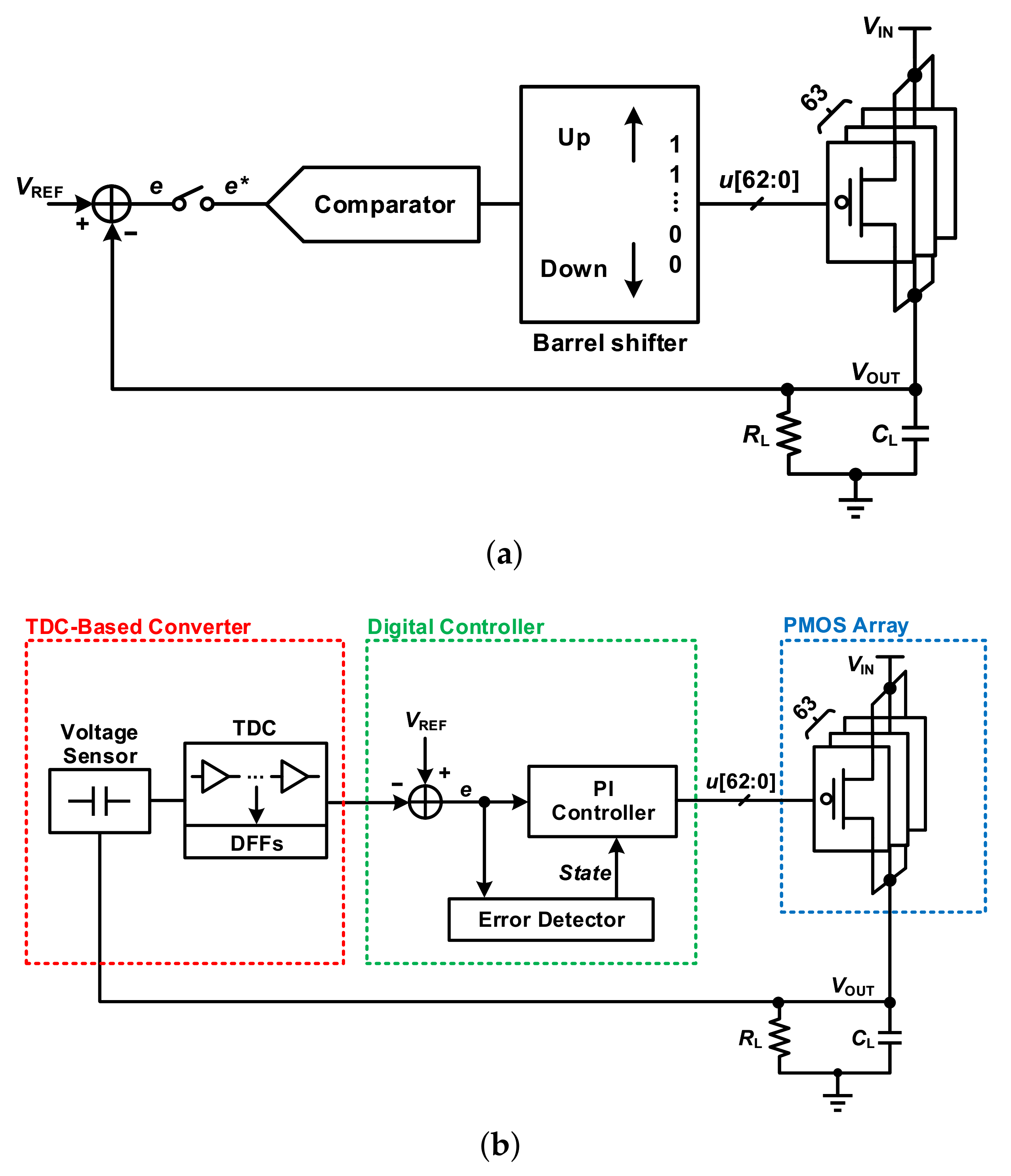
2. Architecture of the Proposed D-LDO

2.1. Topology

Figure 1 shows the circuit diagram for the baseline D-LDO and the proposed D-LDO. The baseline D-LDO employs a comparator and a barrel shifter, whose output code switches 1 bit in a clock cycle. In order to speed up the response, a TDC-Based Converter and an adaptive PI controller are used. The first component is the TDC-based Converter, which provides a digital code of the output voltage V OUT . In the TDC-based converter, a voltage sensor firstly converts the output voltage ( V OUT ) to a time signal by capturing the charging time of a capacitor. The TDC includes the buffers and D-Flip-Flops, converting the time signal to a 63-bit width thermometer code furtherly. Then, the second component is the Digital Controller which consists of a subtractor, an error detector and a PI controller. The subtractor in the digital controller outputs the error between the thermometer code V OUT and the reference voltage V REF . The error is transmitted to the PI controller and the error detector. Together with a S t a t e code calculated by the error detector, the PI controller determined the number of turned-on transistors in the following PMOS array which contains 63 identical PMOS devices controlled by the digital code supplied currents. The proportion and integral coefficients of the PI controller are selected adaptively according to fuzzy rules based on the error and the integral of the error. In this way, the PI controller produces 63-bit width thermometer codes to control the gate of the power transistors in the PMOS array, so that the right amount of current is supplied to the load. The major building blocks of the proposed architecture above will be illustrated in Section 3.

2.2. Transfer Function of the Control Loop

Figure 2 shows the hybrid model for the proposed D-LDO. The relationship between input and output of the TDC-based converter is modeled as a gain K TDC and a zero order holder (ZOH) as interface between continue signal and discrete signal. The z-domain transfer function of the digital controller is derived by taking the traditional z-transfer of the PI controller and is given as
G PI ( z ) = ( K p + K Adjust ) + ( K i + K Adjust ) z 1 1 z 1
where K Adjust is the adaptive coefficient. The output stage and load can be approximated as an RC circuit, and the z-domain model of load and PMOS array is
G LP ( z ) = F LOAD z z e F LOAD / F S
where F LOAD = 1 / ( 2 π · R LOAD · C LOAD ) , F S is sampling frequency. The K P and K i with K Adjust can be represented as K P and K i . V REF is considered as AC ground so the closed-loop transfer function of the D-LDO in z-domain is derived as
G z = K p z K p K i 1 + F LOAD z 1 1 + K TDC K p 1 + F LOAD z 2 2 + K TDC K p + K TDC K p K i 1 + F LOAD z K p K i K TDC + 1
Consider that K p and K i are adjusted with e r r o r , the stability of the proposed D-LDO is changed in each period. If there is a large e r r o r , the stability is traded off to obtain a faster transient response. In contrast, K p and K i are changed to achieve a more stable regulation when the e r r o r is small.
Figure 3 shows the poles of the proposed system under variable integration gain. As illustrated in Figure 3, a higher integration gain of the PI controller leads loss of stability. According to the traditonal PI theory, large K p leads to qucik adjustment and large K i leads to high accuracy. In adaptive process, a large K p is selected when e r r o r in wide region to approach V REF quickly. In addition, if e r r o r in narrow region, a large K i is chosen for eliminating errors.

3. Circuit Implementation

3.1. Time-to-Digital Based Converter
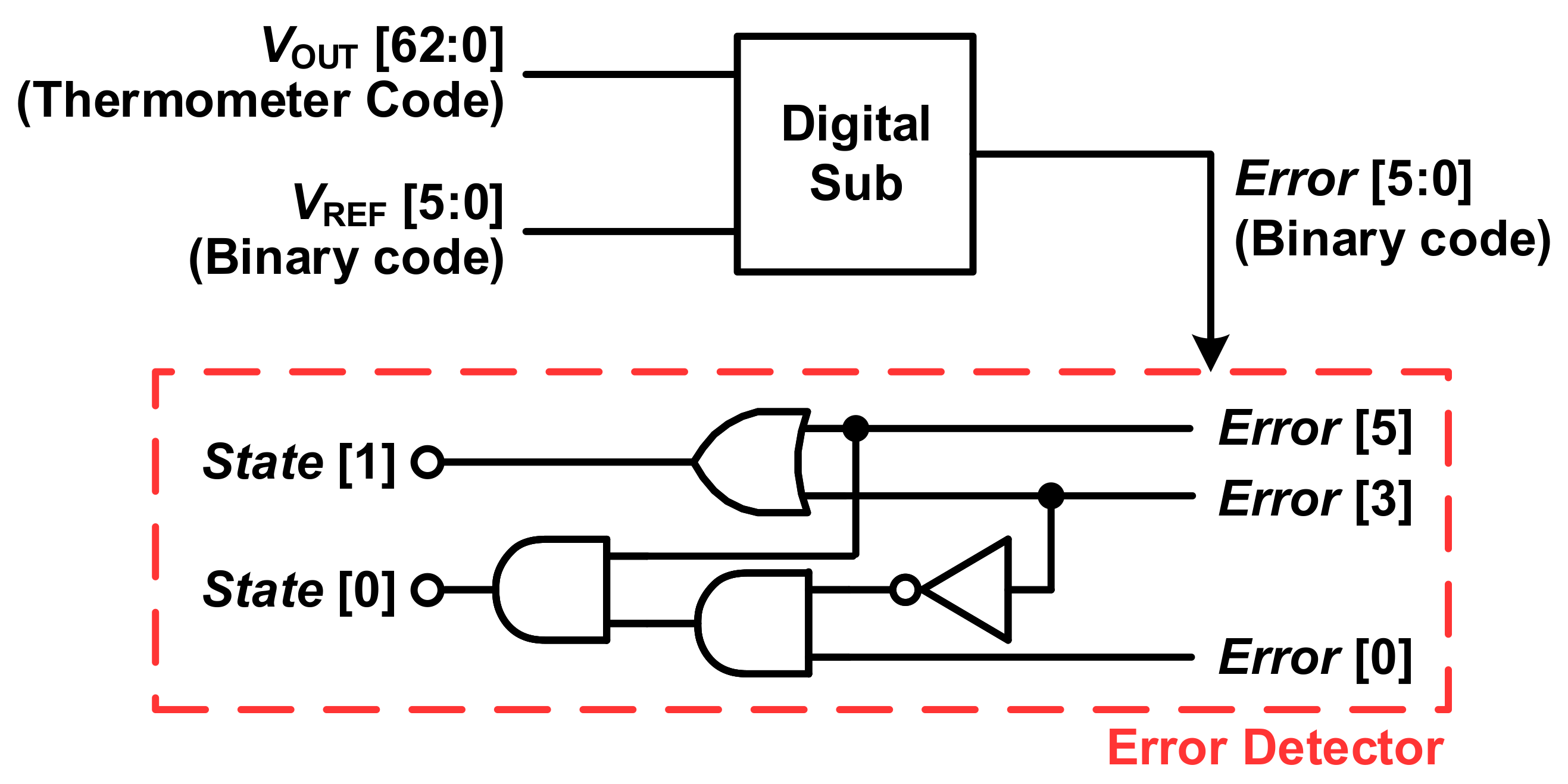
The transformation of the V OUT from analog to digital is based on a voltage sensor and a TDC.
Figure 4 shows the schematics of the voltage sensor which converts the analog signals to time signals. The operation process of voltage sensor consists of two parts. Firstly, when c l k is low level, the switches M0, M1, M5, and M6 are turned on. The capacitor C C is pre-charged with V OUT and V IL which is the trigger voltage of the DFFs which is an information storage device with memory function and two stable states behind. During the charge stage, the quantity of electric charge in C C can be expressed as Q pre = C C · ( V OUT V IL ) . Secondly when c l k is high level, M3, M4, and M6 are turned on, the two plates of C C are connected with GND and current source I C . Because the current loss of C C does not occur suddenly, the charge variation in C C is given as follow
Δ Q = C C · [ V IL ( V IL V OUT ) ] = I C · Δ t
where Δ t is the time from the beginning of charging to the DFFs are triggered. Hence, the voltage sensor converts V OUT to a time signal Δ t .
Figure 5 shows the schematics of the TDC. During the time of Δ t , the input signal “1” is transmitted in the delay line. When the pin O U T generates a positive edge, in other words, the time Δ t is consumed, the DFFs are triggered. The number of DFFs output signal “1” is expressed as N = [ Δ t / t d ] , where t d is the delay time of a buffer. The buffers and DFFs showed in Figure 5 are suitable for standard cell-based logic synthesis.
From the discuss above, an analog signal of V OUT is converted to a signal about time through the operation of voltage sensor when c l k in low level. After c l k is switched to high level, the time signal is transmitted to the TDC for generating digital codes. At the end of a cycle, 63-bit digital thermometer code is obtained. Figure 6 shows the linearity of the proposed TDC-based converter. The test points are fitted into a quadratic function. The different value of V O U T is converted to digital code and the a quantization interval of the TDC-based converter is about 25 mV.

3.2. Error Detector

The adaptive operation in the proposed D-LDO adjusts the coefficients of P and I which is ducted by the error detector as shown in Figure 7. In this mode, the e r r o r between V OUT and V REF is divided into four ranges. The four ranges correspond to four groups of coefficients for the PI controller. Therefore, using the PI digital controller with an error detector, the proposed D-LDO achieves a faster response time and lower overshoot/undershoot voltage.
A digital sub is introduced to generate the error between the V OUT and V REF . Because the output of the TDC-based converter is thermometer code and the reference voltage is binary, the digital sub contains a encoder to convert the output of the TDC-based converter to binary codes. The entire digital sub is implemented by Verilog and logical synthesis.
Four levels for error are shown in Table 1: E r r o r 32 , E r r o r 8 , E r r o r 1 , E r r o r = 0 , where the digital code is equivalent to the thermometer code from the TDC-based converter output N. And Δ N = 1 is equivalent to the 25 mV of voltage values. Therefore, the S t a t e [1:0] becomes “11” when E r r o r 0.9 V, and becomes “10” when E r r o r 0.4 V, and becomes “01” when E r r o r < 0.4 V and becomes “00” when achieve stabilivolt. Depending on E r r o r [5], E r r o r [3], E r r o r [0], the PI controller operates in three groups of coefficient as shown in Table 2.
The determination of coefficients is based on the fuzzy algorithm [12,13]. For example, if the e r r o r is “large” then K P = a 1 x + b 1 , here the a 1 and b 1 are the premise parameter in membership functions of the fuzzy sets "large" in the premises. Therefore, we define the relative range of error as [−3, −2, −1, 0, 1, 2, 3] corresponding to [Negative large, Negative mid, Negative small, Zero, Positive small, Positive mid, Positive large]. To confirm the parameter, we divide the spaces into some fuzzy subspaces where the performance index is minimized.
As mentioned in Section 2, the large K i leads instability. In order to speed up the rate of regulation, a large K p is chosen. Hence, we expect K i will not generate overshoot when the system is regulated quickly. Hence, we select the value of K i is less than 1 when the error is large. On the contrary, when the V OUT close to reference, a large K i and a small K p are needed to eliminate the error and avoid the underdamping. That’s the fuzzy principle to design the value of K p and K i . Through the simulation and the experience of the control system, the final parameters are obtained to calculate the coefficients in Table 2.

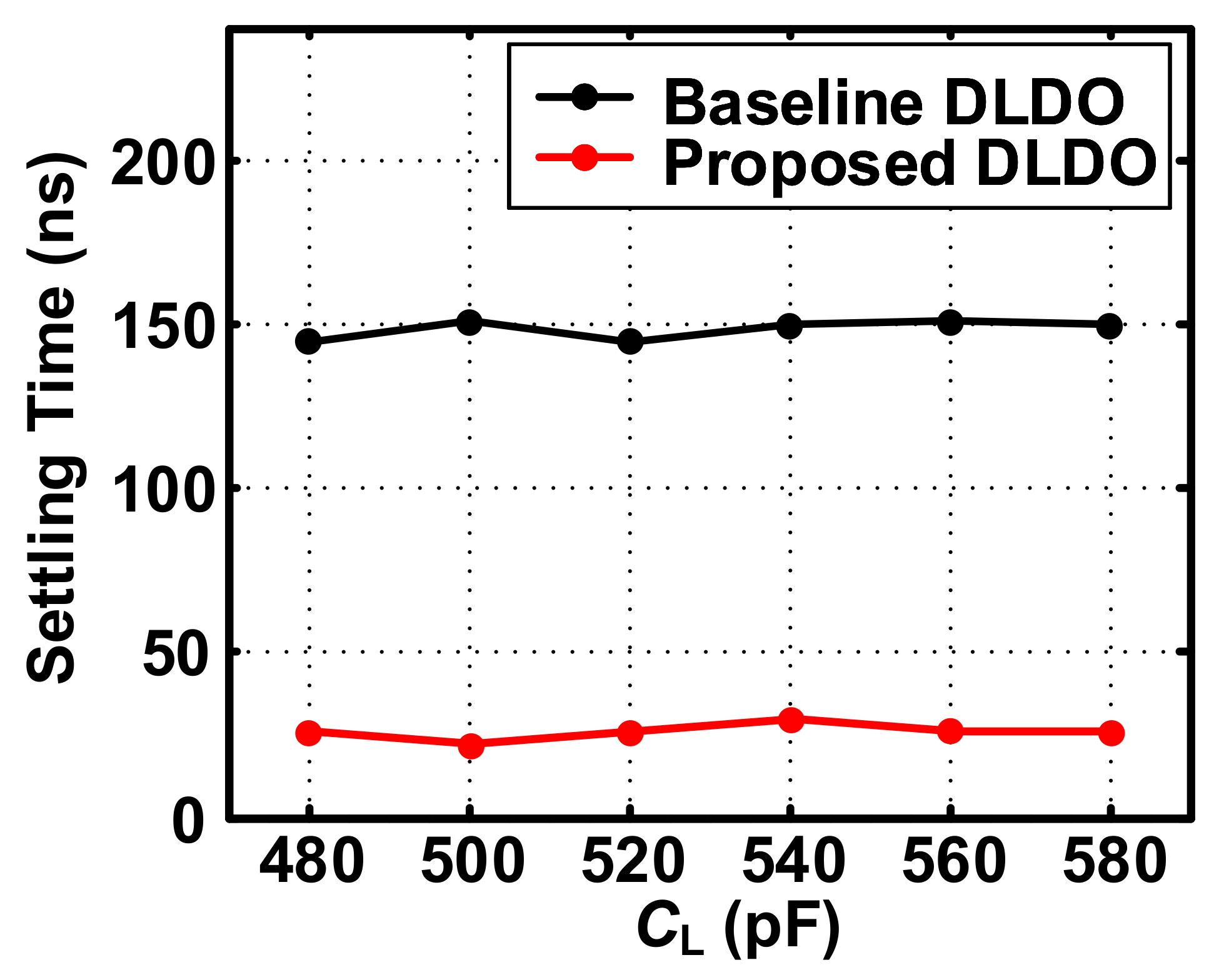
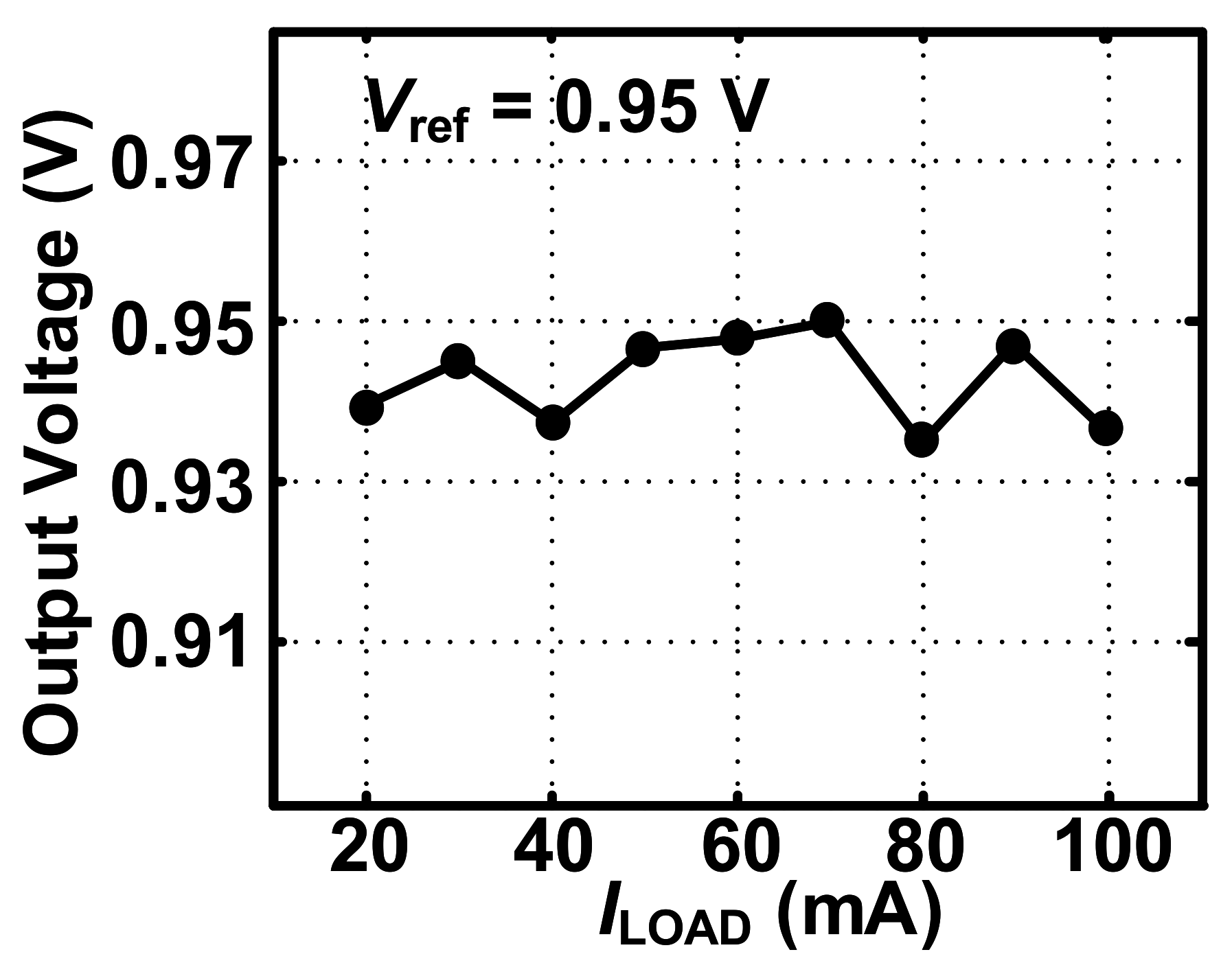
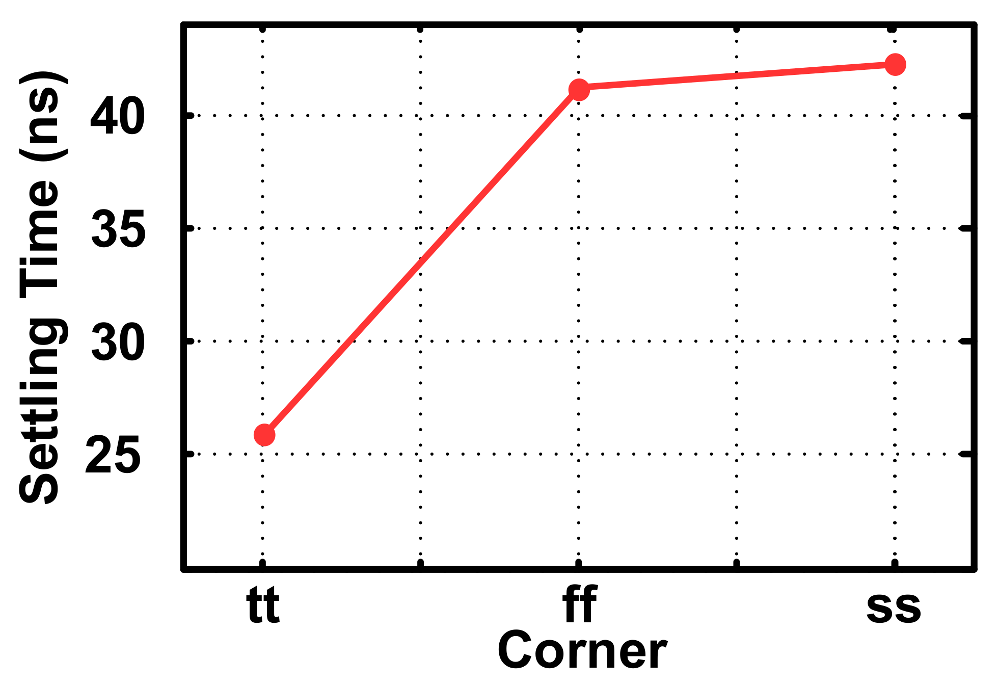
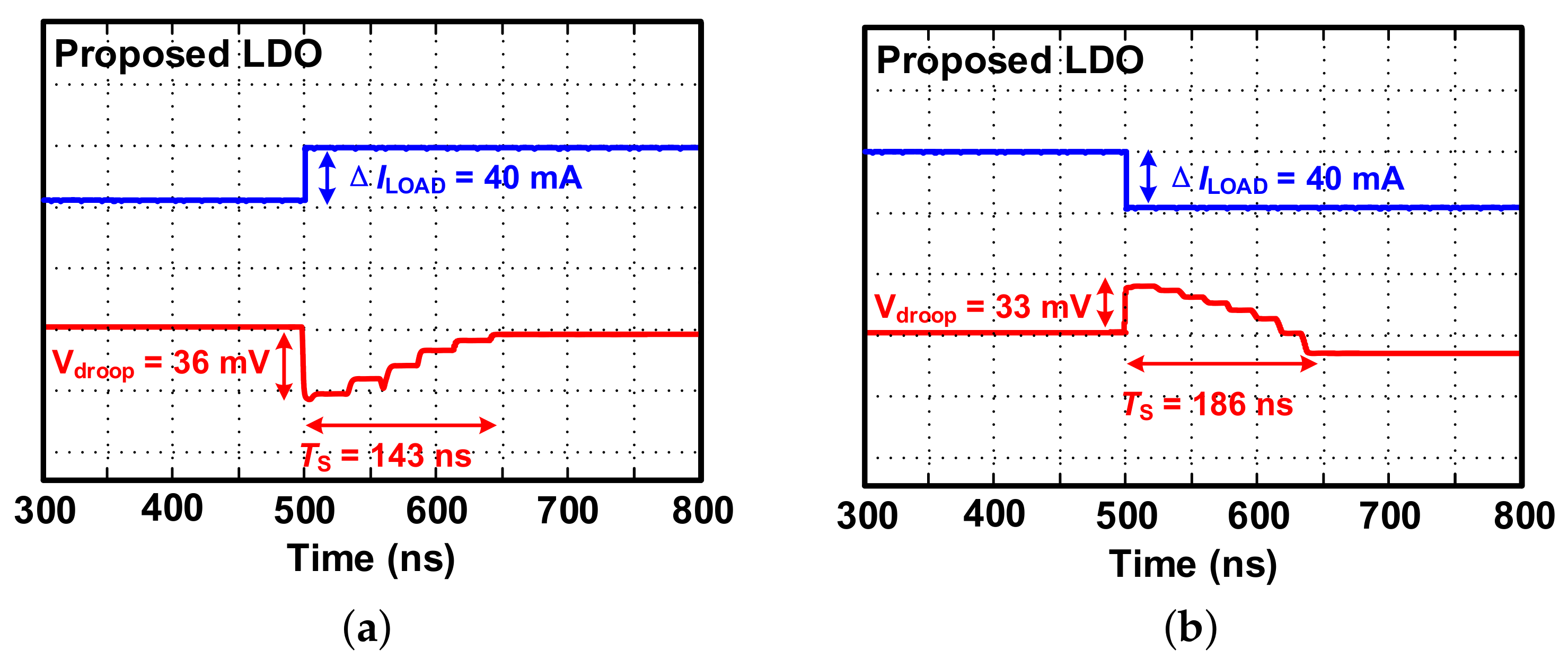
4. Simulation Results and Discussion

The proposed adaptive D-LDO is realized in 180-nm SMIC technology as shown in Figure 8 and the area is 235 μ m × 312 μ m. In the circuit, the charing capacitor C C is 450 fF and the charging current I C is 100 μ A. The delay of each buffers t d is 0.145 ns. The D-LDO operates within an input voltage range of 1–1.2 V and an output voltage of 0.95 V. The D-LDO supplies a maximum current of 100 mA with a load capacitance of 500 pF, while operating at a 40 MHz clock rate with a quiescent current of 34.68 μ A. Simulated current efficiency is 99.64% at 10 Ω load resistor.
In order to describe the transient response speed of the proposed circuit, the settling time T S with variable load was simulated. The settling time is defined as the time that the output voltage recovers to 90% of the droop voltage. As shown in Figure 9 and Figure 10, the proposed D-LDO reduces the settling time under each condition. The settling time is decreased to only 17.6% of the baseline design of D-LDO (from 147.8 ns to 26.1 ns) on average in corner tt which means typical corner. In other words, the proposed circuit improves the response speed by about 5 times.
As shown in Figure 11 and Figure 12, the output voltage with a load current range from 20 to 100 mA and a line voltage range from 1 to 1.2 V are simulated. The effect of the load current and the line voltage on the output voltage is not slight, a load regulation of 0.3 mV/mA and a line regulation of 0.1 mV/mV are achieved. Due to the quantization interval of the TDC-based converter is about 25 mV, the output voltage error in variations of simulation environment is acceptable.
Figure 13 shows the simulated settling time in various corners. With V IN = 1 V and V OUT = 0.95 V, corner tt achieves 26.1 ns, corner ff and ss which means fast or slow corner achieve 42 ns and 44 ns, respectively. It shows the proposed D-LDO has consistency in different conditions.
The simulated output transient response for the load current change with 40 mA in 1 ns in Figure 14. With V in = 1 V, V OUT = 0.95 V (both step up and down), f S = 40 MHz, C L = 0.5 nF, R L = 10 Ω , the simulated output undershoot is 36 mV and the overshoot is 33 mV. Recovery time achieves 143/186 ns within undershoot/overshoot. Compared with the published LDO designs with PI controller, the proposed D-LDO exhibits a significantly faster settling time.
The response time T R of the D-LDO is proposed in [14] is given as
T R = C L Δ V OUT I MAX
where C L is the load capacitance, Δ V OUT is the undershoot/overshoot voltage, I MAX is the maximum load current. Commonly used figure-of-merits FOM1 and FOM2 [14] for LDO performance is
FOM 1 = C L Δ V OUT I MAX · I Q I MAX
FOM 2 = Δ V OUT V OUT · I Q I MAX · C L
where I Q is the quiescent current. The smaller FOM indicates the better LDO performance.
The comparison with published D-LDOs are listed in Table 3. In comparison to those prior designs, the proposed D-LDO achieves FOM1 of 0.65 ps, FOM2 of 0.068 pF, and T R of 0.18-ns. In contrast to these prior D-LDOs, this paper achieves faster response time, lower undershoot/overshoot voltage, and more outstanding performance on the figure-of-merit FOM1 and FOM2. Meanwhile, the proposed D-LDO exhibits decent competitive current efficiency.

5. Conclusions

A fully integrated D-LDO with fast transient response is proposed. The D-LDO is designed and simulated in 180-nm technology. With an error detector, the proposed D-LDO achieves an undershoot of 36 mV, overshoot of 33 mV, and transient response time of 143/186 ns for a load change with a 40 mA/ns slew rate. The multi-bit conversion technique decreases the settling time in corner tt, ff, ss to 17.6%, 27.3%, and 28.6% of the baseline D-LDO respectively. The current consumption is 34.68 μ A and the peak current efficiency is 99.64%. The proposed D-LDO achieves FOM1 of 0.65 ps and FOM2 of 0.068 pF, which are comparable with the state-of-the-art designs.

Author Contributions

Conceptualization, S.L., H.Z. and Z.C.; Data curation, S.L., H.Z. and J.G.; Investigation, P.W., J.W. and Y.Y.; Methodology, S.L., H.Z. and Z.C.; Resources, P.W. and Z.C.; Writing—original draft, S.L., H.Z. and Z.C.; and Writing—review and editing, S.L., H.Z., P.W. and Z.C.; All authors have read and agreed to the published version of the manuscript.

Funding

This work was supported by Beijing Natural Science Foundation Project No. 4202010, and National Natural Science Foundation of China, Key Project No. 61731019.

Data Availability Statement

The data presented in this study are available on request from the corresponding author.

Conflicts of Interest

The authors declare no conflict of interest.

References

  1. Lam, Y.H.; Ki, W.H. A 0.9 V 0.35 µm Adaptively Biased CMOS LDO Regulator with Fast Transient Response. In Proceedings of the 2008 IEEE International Solid-State Circuits Conference—Digest of Technical Papers, San Francisco, CA, USA, 3–7 February 2008; pp. 442–626. [Google Scholar]
  2. Milliken, R.J.; Silva-Martinez, J.; Sanchez-Sinencio, E. Full On-Chip CMOS Low-Dropout Voltage Regulator. IEEE Trans. Circuits Syst. I Regular Pap. 2007, 54, 1879–1890. [Google Scholar] [CrossRef]
  3. Nasir, S.B.; Gangopadhyay, S.; Raychowdhury, A. All-Digital Low-Dropout Regulator With Adaptive Control and Reduced Dynamic Stability for Digital Load Circuits. IEEE Trans. Power Electron. 2016, 31, 8293–8302. [Google Scholar] [CrossRef]
  4. Ojima, N.; Nakura, T.; Iizuka, T.; Asada, K. A Synthesizable Digital Low-Dropout Regulator Based on Voltage-to-Time Conversion. In Proceedings of the 2018 IFIP/IEEE International Conference on Very Large Scale Integration (VLSI-SoC), Verona, Italy, 8–10 October 2018; pp. 55–58. [Google Scholar]
  5. Woo, K.; Kim, T.; Hwang, S.; Kim, M.; Yang, B. A fast-transient digital LDO using a double edge-triggered comparator with a completion signal. In Proceedings of the 2018 International Conference on Electronics, Information, and Communication (ICEIC), Honolulu, HI, USA, 24–27 January 2018; pp. 1–4. [Google Scholar]
  6. Salem, L.G.; Warchall, J.; Mercier, P.P. A 100 nA-to-2 mA successive-approximation digital LDO with PD compensation and sub-LSB duty control achieving a 15.1 ns response time at 0.5 V. In Proceedings of the 2017 IEEE International Solid-State Circuits Conference-(ISSCC), San Francisco, CA, USA, 5–9 February 2017; pp. 340–341. [Google Scholar]
  7. Amayreh, M.; Leicht, J.; Manoli, Y. A 200ns settling time fully integrated low power LDO regulator with comparators as transient enhancement. In Proceedings of the 2016 IEEE International Symposium on Circuits and Systems (ISCAS), Montreal, QC, USA, 22–25 May 2016; pp. 494–497. [Google Scholar]
  8. Ding, Z.; Rhee, W.; Wang, Z. A VCO-dedicated digital LDO with multi-comparator coarse loop and 1-bit Δ∑ fine loop for robust frequency generation. In Proceedings of the 2018 IEEE MTT-S International Wireless Symposium (IWS), Chengdu, China, 6–10 May 2018; pp. 1–4. [Google Scholar]
  9. Lu, Y.; Huang, M.; Martins, R.P. PID Control Considerations for Analog-Digital Hybrid Low-Dropout Regulators (Invited Paper). In Proceedings of the 2019 IEEE International Conference on Electron Devices and Solid-State Circuits (EDSSC), Xi’an, China, 12–14 June 2019; pp. 1–3. [Google Scholar]
  10. Kim, D.; Seok, M. A fully integrated digital low-dropout regulator based on event-driven explicit time-coding architecture. IEEE J. Solid State Circuits 2017, 52, 3071–3080. [Google Scholar] [CrossRef]
  11. Lim, C.; Mandal, D.; Bakkaloglu, B.; Kiaei, S. A 50-mA 99.2% Peak Current Efficiency, 250-ns Settling Time Digital Low-Dropout Regulator with Transient Enhanced PI Controller. IEEE Trans. Very Large Scale Integr. VLSI Syst. 2017, 25, 2360–2370. [Google Scholar] [CrossRef]
  12. Santos, M.; Dormido, S.; de la Cruz, J.M. Fuzzy-PID controllers vs. fuzzy-PI controllers. In Proceedings of the IEEE 5th International Fuzzy Systems, New Orleans, LA, USA, 11 September 1996; Volume 3, pp. 1598–1604. [Google Scholar]
  13. Takagi, T.; Sugeno, M. Fuzzy identification of systems and its applications to modeling and control. IEEE Trans. Syst. Man Cybern. 1985, 116–132. [Google Scholar] [CrossRef]
  14. Hazucha, P.; Karnik, T.; Bloechel, B.A.; Parsons, C.; Finan, D.; Borkar, S. Area-efficient linear regulator withultra-fast load regulation. IEEE J. Solid State Circuits 2005, 40, 933–940. [Google Scholar] [CrossRef]
  15. Yuan, Z.; Fan, S.; Geng, L. A 225-mA Binary Searching Digital LDO with Transient Enhancement. In Proceedings of the 2019 IEEE International Conference on Electron Devices and Solid-State Circuits (EDSSC), Xi’an, China, 12–14 June 2019; pp. 1–2. [Google Scholar]
  16. Yuan, Z.; Fan, S.; Yuan, C.; Geng, L. A 100 MHz, 0.8-to-1.1 V, 170 mA Digital LDO with 8-Cycles Mean Settling Time and 9-Bit Regulating Resolution in 180-nm CMOS. IEEE Trans. Circuits Syst. II Express Briefs 2020, 67, 1664–1668. [Google Scholar] [CrossRef]
  17. Chen, W.-J.; Huang, C.-H. Fast-Turnaround Design and Modeling Techniques for a Fast-Transient Digital Low-Dropout Regulator With 3 mV Ripples. IEEE Trans. Power Electron. 2021, 36, 6824–6837. [Google Scholar] [CrossRef]
Figure 1. The circuit architecture of (a) the baseline D-LDO and (b) the proposed D-LDO.
Electronics 10 01668 g001
Figure 2. The system hybrid model for the proposed D-LDO.
Electronics 10 01668 g002
Figure 3. The pole plot of the proposed system under variable integration gain (x shown in Figure 3).
Electronics 10 01668 g003
Figure 4. Schematics of the Voltage Sensor.
Electronics 10 01668 g004
Figure 5. Schematics of the Time-to-Digital Converter.
Electronics 10 01668 g005
Figure 6. The linearity of proposed TDC-Based converter.
Electronics 10 01668 g006
Figure 7. Schematics of the Error Detector.
Electronics 10 01668 g007
Figure 8. The layout of the proposed D-LDO.
Electronics 10 01668 g008
Figure 9. The settling time with load capacitance change.
Electronics 10 01668 g009
Figure 10. The settling time with I LOAD change.
Electronics 10 01668 g010
Figure 11. The output voltage under the variations of load current.
Electronics 10 01668 g011
Figure 12. The output voltage under the variations of line voltage.
Electronics 10 01668 g012
Figure 13. The settling time with corner change.
Electronics 10 01668 g013
Figure 14. The transient responses of V OUT when I LOAD change of (a) step up and (b) step down.
Electronics 10 01668 g014
Table 1. State table. 1 means high voltage, 0 means low voltage, X means any voltage.
Error LevelsInputOutput
Error[5]Error[3]Error[0]State[1]State[0]
Error ≥ 321XX11
Error ≥ 801X10
Error ≥ 100101
Error = 000000
Table 2. Cofficient.
InputOutput
State[1]State[0]PI
00Hold onHold on
010.84
1010.7
111.20.1
Table 3. Comparison with published D-LDO designs.
DesignYuan [15],
EDSSC’19
Yuan [16],
TCSII’20
Chen [17],
TPEL’21
This Work
Process180-nm180-nm110-nm180-nm
V IN (V)10.8–1.10.8–1.21–1.2
V OUT (V)0.90.7–1.00.7–1.10.95
Load Regulation (mV/mA)0.0530.110.4220.3
Current Consumption ( μ A)500500188.8–197.934.68
Total C L Not available390 pF40 pF0.5 nF
Δ V OUT @ Δ I LOAD
420 mV
@216 mA

267 mV
@160 mA

360 mV
@47.5 mA
36 mV
@40 mA
Load Transient Edge Time (ns)NA65<11
Recovery Under/Over-shoot Time (ns)80/8080/8067/250143/186
Peak Current Efficiency (%)99.7899.7192.98–99.6199.64
Response Time T R (ns)0.950.520.20.18
FOM1 (ps)2.12.031.260.65
FOM2 (pF)Not available0.3620.07060.068
Publisher’s Note: MDPI stays neutral with regard to jurisdictional claims in published maps and institutional affiliations.

