Article

Scalable Multiport Converter Structure for Easy Grid Integration of Alternate Energy Sources for Generation of Isolated Voltage Sources for MMC

1
Department of Electrical and Computer Engineering, Texas A&M University, College Station, TX 77843, USA
2
Clean and Resilient Energy Systems (CARES) Lab, Texas A&M University, Galveston, TX 77554, USA
3
Department of Electrical Engineering, Aligarh Muslim University, Aligarh 202002, India
4
Department of Electrical Engineering, College of Engineering, Taif University, Taif 21944, Saudi Arabia
5
Department of Electrical Engineering, Qatar University, Doha 2713, Qatar
*
Author to whom correspondence should be addressed.
Electronics 2021, 10(15), 1779; https://doi.org/10.3390/electronics10151779
Submission received: 24 June 2021 / Revised: 17 July 2021 / Accepted: 23 July 2021 / Published: 25 July 2021
(This article belongs to the Special Issue Modeling, Control, and Optimization of Power Electronics)

Abstract

:
This paper presents a novel, scalable, and modular multiport power electronic topology for the integration of multiple resources. This converter is not only scalable in terms of the integration of multiple renewable energy resources (RES) and storage devices (SDs) but is also scalable in terms of output ports. Multiple dc outputs of a converter are designed to serve as input to the stacking modules (SMs) of the modular multilevel converter (MMC). The proposed multiport converter is bidirectional in nature and superior in terms of functionality in a way that a modular universal converter is responsible for the integration of multiple RES/SDs and regulates multiple dc output ports for SMs of MMC. All input ports can be easily integrated (and controlled), and output ports also can be controlled independently in response to any load variations. An isolated active half-bridge converter with multiple secondaries acts as a central hub for power processing with multiple renewable energy resources that are integrated at the primary side. To verify the proposed converter, a detailed design of the converter-based system is presented along with the proposed control algorithm for managing power on the individual component level. Additionally, different modes of power management (emulating the availability/variability of renewable energy sources (RES)) are exhibited and analyzed here. Finally, detailed simulation results are presented in detail for the validation of the proposed concepts and design process.

1. Introduction

For the realization of high voltage–high power operations with increased reliability, a multilevel inverter approach is usually preferred. A multilevel approach for voltage source inverters results in low dV/dt stress and reduced voltage ratings for semiconductor switches, hence, reduced cost, low harmonics content (due to high resultant switching frequency), and smaller ripple currents (at high frequencies, system impedance increases) that result in reduced size/cost for input and output filter inductors [1,2,3]. All conventionally used converters have an integrated operation and need to be shut down in case of a device/control failure that results in significant production loss in the industry. In such cases, modularity may provide a better alternative. Conventionally, three basic types of multilevel converters are used, i.e., diode clamped, flying capacitor, and cascaded H bridge. These converters have different tradeoffs such as active/reactive power compensation, efficiency, scalability, modularity, components count, cost, and total harmonic distortion (THD) content. Considering these facts, a cascaded H Bridge is usually preferred for most electric machine drives and their related applications. However, cascaded H Bridge (CHB) and H Bridge Neutral Point clamped (HNPC) converters usually need a phase shift transformer with multiple secondary windings to generate DC voltages for each sub-module. This transformer often aids in isolation needs but makes the system bulky, lossy, and costly along with the inability to improve power quality [1,2,4,5,6,7].
The modular multilevel converter is a promising technology for medium and high-voltage applications. The major features of the MMC are modularity, voltage and power scalability, fault resilient operation, and high-quality waveforms with minimized electromagnetic interference [8,9,10,11]. Due to these excellent features, MMC have made excellent inroads into different application fields. Implementation and control of MMCs for reactive power management (as a STATCOM) and active end applications are also presented in the literature [12,13]. The most path-breaking application of this converter is in the field of high-power HVDC transmission. It has significantly impacted both onshore and offshore transmission models [14]. The application of IGCT based MMC is also presented in the literature [15]. The application of MMCs for power flow management in hybrid microgrids is also discussed [16,17,18,19]. In all of these applications, although significant performance benefits are obtained, balancing each submodule capacitor poses a significant challenge. Extensive literature has been discussed to address this voltage balancing issue [16,20,21].
Over the past few years, several research studies have been conducted to address the technical challenges associated with the operation and control of MMCs, including modulation techniques. The major challenge in the topology is the requisite of complex control necessities that consider simultaneous control of (i) the generation of proper current reference to load requirement, (ii) the output currents, (iii) maintaining dc voltage in agreement with a reference value, and (iv) capacitor voltage balancing among the sub-modules [16,17,22]. Additionally, large sub-module capacitors are also required for limiting capacitor voltage variations. Furthermore, the efficiency is very much dependent on modulation and the selection of the sub-module [23,24,25,26,27].
Currently, there are two major power processing challenges linking MMCs and distributed energy source integration to the utility grid. In this paper, the authors have proposed a modular power converter structure for integration of different energy sources (including renewable, storage, and conventional utility grids) to produce isolated power supplies for each MMC sub-module. The structure is based on two most well-defined converters, namely the boost converter and the high-frequency transformer based multiport active bridge converter. Multiple RES and storage devices (SDs) can be connected on the primary side DC-link along with the rectified voltage feed from the AC grid, as shown in Figure 1. These submodules that are shown consist of individual inverters, modules to obtain multi-level voltage across a medium-voltage ac load.
There are several advantages related to the proposed topology. Modularity can be easily achieved, and power flowing in the secondary winding can be independently controlled [28,29,30]. This eliminates any unbalancing issues in the MMC sub-modules. Another advantage is the employment of a high–frequency central transformer, which results in space and cost-saving compared to CHB and HNPC. On top of this, bidirectional operation from the secondary side dc link to the primary side resource (charging battery storage) can be achieved simply by changing the phase shift between the PWMs of the primary and secondary side H bridges of the respective DAB [28,31,32,33].
The remaining paper is structured as follows: Section 2 discusses the proposed converter topology. Section 3 presents the detailed design of the different components of the system. Section 4 briefs the control algorithms and operation modes possible within the system. In Section 5, detailed simulation results are provided, which evaluate the system performance in different modes of operation. Finally, Section 6 concludes the findings of the proposed work.

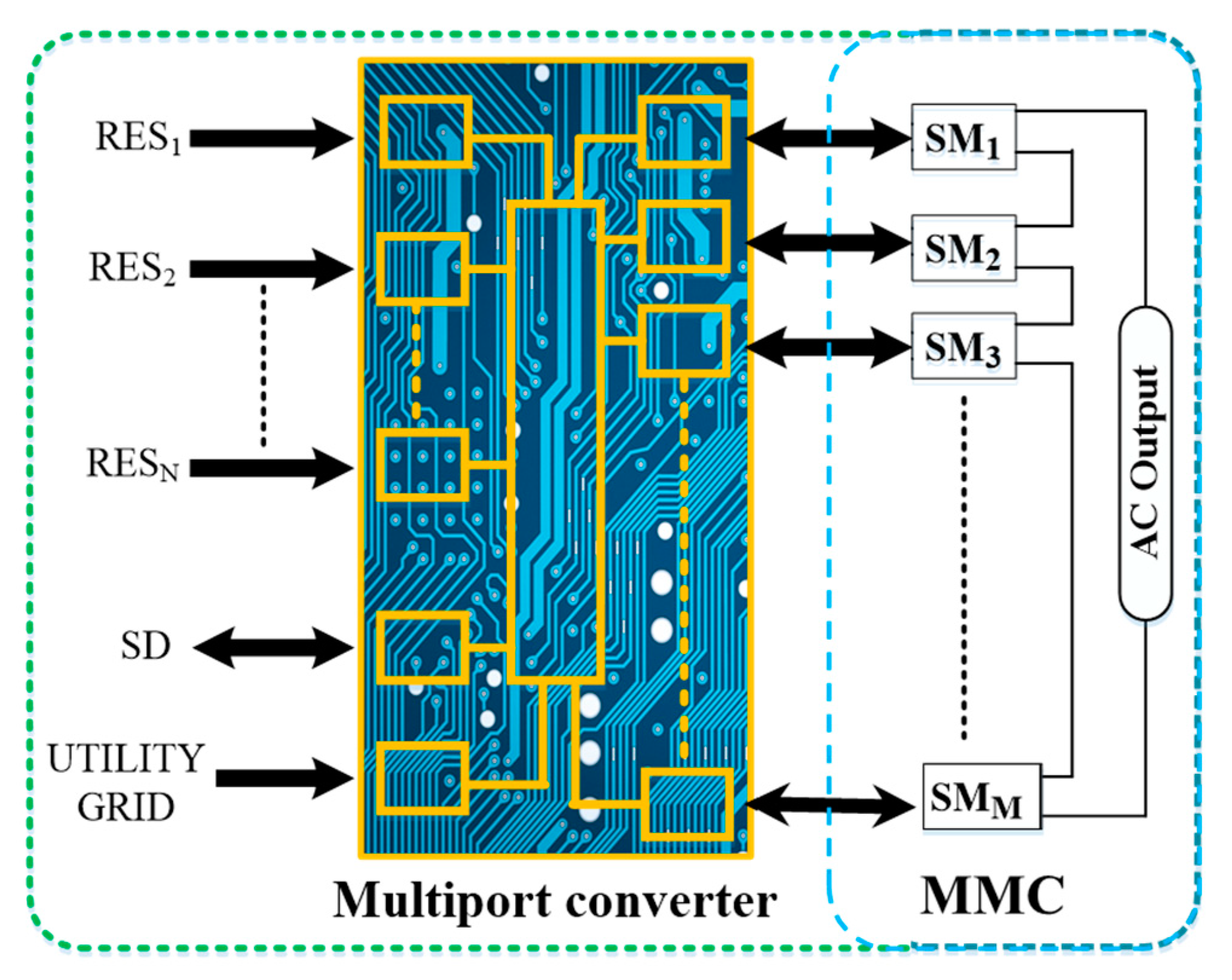
2. Description of Microgrid under Consideration

The detailed circuit diagram of the proposed converter is shown in Figure 2. It mainly consists of three components:
(i)
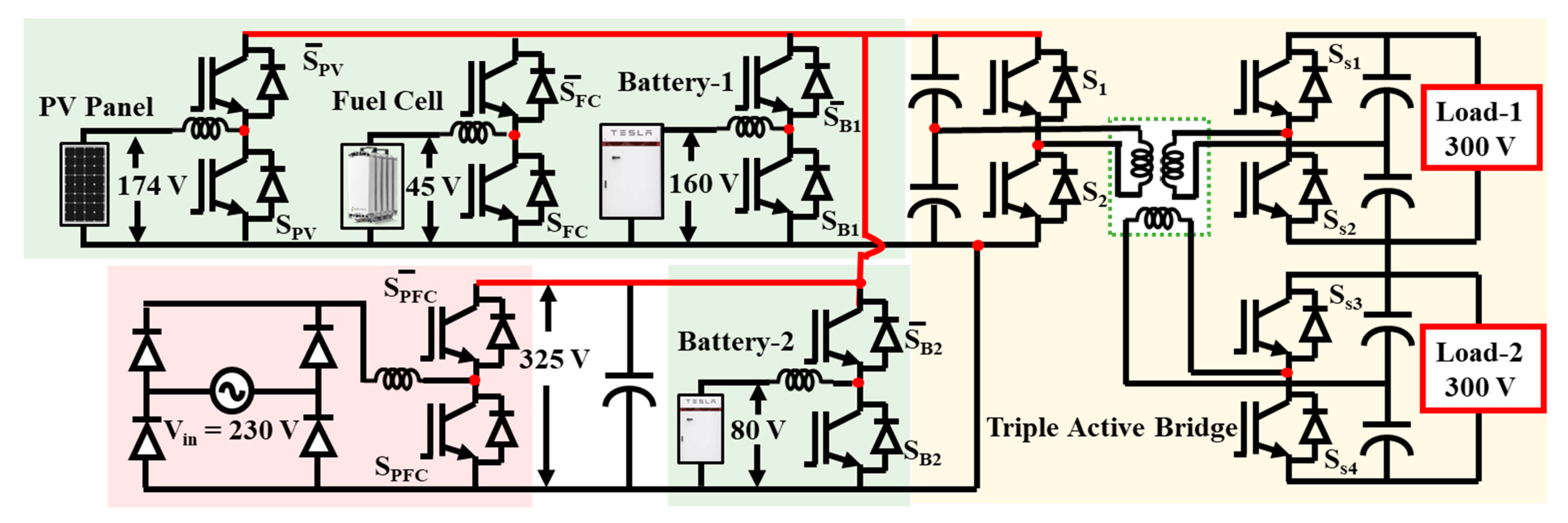
A triple active half-bridge converter is capable of bidirectional dc–dc conversion. It consists of a high-frequency transformer with a single primary and multiple secondary windings. Half-bridge with doubler capacitors, realizing a triple active half-bridge circuit, is employed on both sides. Symmetrical cascaded semi-active bridges are extendable for multilevel conversion operations.
(ii)
Green utility grid circuit consisting of diode-based rectifier followed by boost converter-based power factor correction circuit. This helps to achieve the unity power factor operation along with the minimized harmonic contents.
(iii)
Boost converter-based integrated renewable energy sources (PV panel and fuel cell stacks) and battery storages (Battery–1 and Battery–2) supplying power to the load depending upon the availability.
First, optimum operation of the RES (at the respective MPPT points) and SD power flow must be ensured by developing a proper control algorithm at each circuit level. This results in different designs and implementations of the modular boost converter depending on the energy source it is connected to. Second, the power required by the output dc loads must be controlled such that the power consumed from the utility grid is minimized. Another possibility (although not in the scope of the present paper) would be controlling the three active bridges to direct power flow between the two dc buses (such that the leading bus delivers the power to the lagging bus).

3. Design of Different Components of the System

A.
Diode Rectifier: A grid voltage of 230 V, 60 Hz, is connected at the input of the diode bridge rectifier. A peak grid voltage of 325 V must be obtained at the output, assuming that a big capacitor is placed at the output. This means that the voltage blocking capacity of the diodes must be at least 325 V. Conclusively, the diode of a 600 V rating must be selected (considering safety margin). On the other hand, as boost power factor correction is used at the output of the rectifier, the grid current is sinusoidal under all operating conditions. Thus, the current rating of the diode must be equal to the full load current contributed by the utility grid alone with no other power source operating.
Design of Power Factor Correction Circuit: To achieve a voltage ripple of a 2% of peak grid voltage, the capacitor required is calculated to be [34]:
C = P o u t 2 × η × V o u t 2 × ( R F v ) × ω
where Pout is the rated output power, RFv designates the voltage ripple, ω is the grid frequency, and Vout is the rectifier output voltage. Substituting these values, the capacitor value is obtained to be 1.3 mF. Thus, the selected capacitor must be rated for 1.5 mF, 600 V.
The inductor value required to obtain a 10% current ripple in the grid current waveform is given by [34]:
L s = V o u t 4 × f × ( R F i ) × I s
where f is the switching frequency (restricted to 20 kHz) and Is refers to the rms value of the grid current (9.15 A in this case). Substituting these values, we obtain the value of the inductor to be approximately 4.5 mH. Thus, the rating of the inductor is selected to be 5 mH, 20 A. The boost switch and boost diode are rated for peak grid voltage and peak grid current. Thus, the rating of each is selected to be 600 V, 20 A, and the diode must have a fast reverse recovery characteristic.
B.
Design of Half-Bridge DAB Converter [35]: The design of the half-bridge DAB converter must be designed for one primary winding and two secondary windings. The primary side DAB is powered from the output voltage of the power factor correction circuit with a peak of grid voltage (325 V). This input voltage is inverted to give ac voltage at the input of the DAB converter, and it is then transmitted to the secondary windings to give two isolated secondary windings. The turns ratio of the windings is maintained as: primary: secondary-1 = 1:1 and primary: secondary-2 = 1:1. The transformer is rated for a maximum power rating of 2 kW (i.e., 1 kW for each secondary). For an input voltage of 230 V (rms), the rms current value is calculated to be 8.7 A for a 100% efficiency assumption. For 95% efficiency, the current at the input of the transformer must have an rms value of 9.15 A. The switching frequency of the DAB converter is selected to be 40 kHz.
For the 1 kW power rating of each secondary with a 100 Ω resistance connected at the load, the output voltage and output current are approximately 325 V and 3.25 A, respectively. A similar voltage and current are also obtained at the other secondary winding. Since the DAB converter uses a half-bridge converter with a voltage doubler at the secondary, the output voltage at the transformer secondary is 162.5 V at each secondary winding. On the primary side, a similar half-bridge circuit is used along with capacitors, which bucks the input voltage to half, i.e., applied dc bus voltage of 325 V is reduced to 162.5 V. This means that the switches on either side of the transformer must be rated for half of the dc-link voltages. Thus, they must be selected to be rated for 300 V (with a considerable margin of safety). Leakage inductance for the transformer winding is calculated by using the formula [30,36]:
L s = V i n × V o u t × ϕ × ( 1 ϕ ) 8 π × f × n × 4 P o
where Po is rated output power, ϕ is the maximum phase shift between primary and secondary winding, Vin is the input voltage applied to the DAB converter, and Vout is the output voltage obtained at the output of the DAB converter. Substituting these values with ϕ = 0.25 (where maximum power transfer occurs), the value of leakage inductance is obtained to be 12 uH. The resistance of the winding is set as 0.02 Ω. Shunt impedance values are assumed to be high and can be neglected.
C.
Design of Boost Converter for Solar PV Panel: Each PV panel used in the simulation model has a maximum power rating of 213 W with its MPPT point being (29 V, 7.35 A). To reach a dc-link voltage of 325 V, six of these PV panels are connected in series to give an input voltage of 174 V at 7.35 A as its MPPT point (1278 W). This means that the MPPT voltage must now be boosted to 325 V using a dc–dc boost converter to ensure controlled and MPPT operation. The voltage rating of the two switches is equal to the dc-link voltage of 325 V, and the current rating can never exceed the maximum panel current rating of 7.84 A. Thus, the two switches are selected to be of 600 V, 10 A rating.
For these specifications, to reach the output voltage of 325 V from maximum input of 174 V (at MPPT), the duty ratio required is D = 0.46. At this duty cycle, for an inductor current ripple of 30% at a switching frequency of 20 kHz, the inductor value is obtained by using the formulae [37]:
L s = V i n × ( V o u t V i n ) f × ( Δ I L ) × V o u t   where   Δ I L = R F i × I o u t ( max ) × V o u t V i n  
Substituting the above values, the inductor value is obtained to be 1.6 mH. Thus, the inductor is selected to be 2 mH, 10 A. For the capacitor design, the formula used is given by [37]:
C o u t ( min ) = D × I o u t ( max ) f × Δ V o u t
For a 1% voltage ripple of 325 V and a 4.6 A maximum output current, the capacitor value is calculated to be 30 µF. Thus, the selected value of the capacitor is rated for 100 µF and 600 V.
D.
Design of Boost Converters for Batteries: The two batteries used in the circuit are rated for 160 V, 10 A and 80 V, 10 A. In the design, the two batteries differ in power rating and the operating duty ratio to achieve the dc-link voltage. To reach dc-link voltage at the output of battery-1 (160 V, 10 A), the duty ratio required is calculated to be 0.51 for the boost converter. For this duty ratio, the inductor and capacitor values are calculated to be 4 mH (10% current ripple) and 38 µF (1% voltage ripple) using (4) and (5), respectively. Thus, the selected inductor and capacitor values are selected to be 5 mH, 15 A, and 100 µF, 600 V.
For battery-2 with the specifications of 80 V, 10 A, the required duty cycle is 0.75. For this duty cycle, with a 20 kHz switching frequency, the inductor and capacitor are estimated to be 3 mH (10% current ripple) and 29 µF (1% voltage ripple). Thus, the inductor value is selected to be 1 mH, 15 A, while the capacitor value is selected to be 100 µF, 600 V.
E.
Design of Boost Converter for Fuel Cell: Fuel cells are characterized by a high current and relatively low voltages compared to other renewable sources. Here, the nominal voltage and current values are 35 A and 45 V, respectively. For these values, the duty ratio is required D = 0.816. Here, the inductor required for a 10% current ripple is estimated to be 553 uH using Equation (4). The rating of the inductor is selected to be 1 mH, 50 A. The capacitor value required for a 1% voltage ripple is calculated to be 64 µF using Equation (5). For this, the capacitor value is selected to be 150 µF, 600 V. The boost switch must be rated for 600 V, 50 A, and the series diode must be rated for 600 V, 50 A (fast recovery).

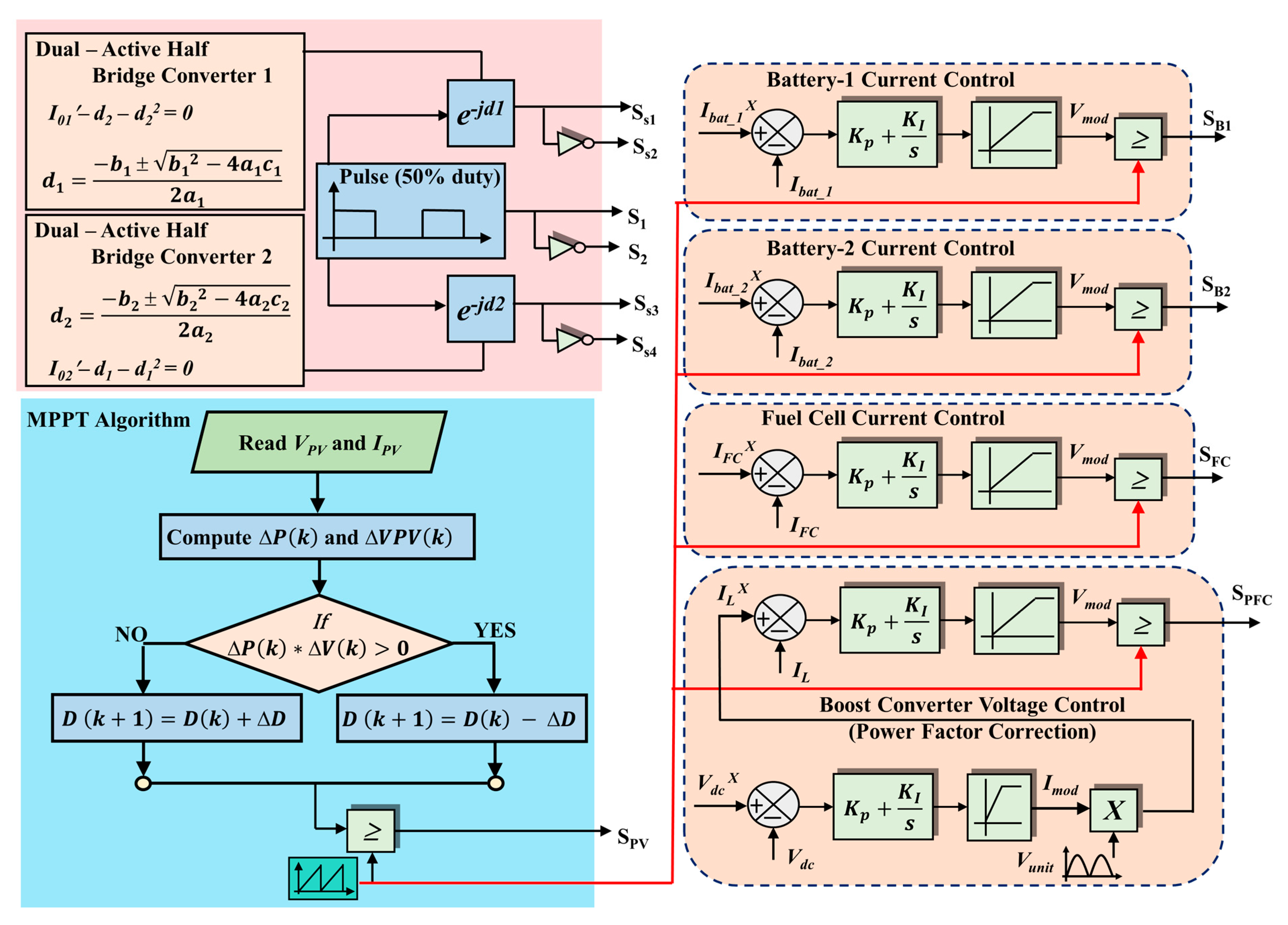
4. Control Algorithm

In the circuit designed above, three types of devices are characteristically different. They are the:
(i)
Unidirectional energy source—utility grid, PV energy source, and fuel cell stacks;
(ii)
Unidirectional Loads—resistive load connected at the output of the triple-active half-bridge outputs;
(iii)
Bidirectional energy source—batteries that can supply/consume power from the utility grid.
For control of the system consisting of multiple energy sources and loads, two levels of control always exist. First, power generation is controlled and managed among the different generators. In this section, first, the control algorithm is first explained on the component level, and certain constraints are then established to simplify the system-level control.
  • Control Algorithm for power factor correction circuit of diode bridge rectifier: The boost circuit is implemented here for the power factor correction of the diode bridge rectifier current. Here, either the hysteresis controller or the PI controller (consisting of two PI controllers) can be used for controlling the grid current. Although the hysteresis controller is fast and reliable, it suffers from variable switching frequency, which affects other components that are connected in the system. Because of the complexity of the system, the PI controller-based control algorithm is adopted here, as shown in Figure 3. First, the output voltage is sensed and compared with the reference value to give the inductor current reference. This inductor current must now have the waveshape of a rectified sine wave in synchronism with the input voltage. To create the desired waveshape, the output voltage of the diode bridge rectifier is sensed and unitized by dividing it with the peak value to obtain a unity signal. This signal is then multiplied with the output of the voltage control loop to obtain the current reference. This current reference is then passed through the current control loop to generate the desired duty cycle. This duty cycle is then compared with a 20 kHz sawtooth carrier signal to generate switching pulses for the boost switch. As mentioned above, a fast recovery semiconductor diode must be used in the boost converter for accurate performance.
  • MPPT Algorithm for control of PV power injection: The power generated by the PV panels must be maximized by operating the circuit at the MPPT point. To achieve this, the panel voltage and panel current must be sensed. These sensed values are then compared with the previous values to obtain ΔP and ΔV. The slope of ΔPV must then be determined. However, this may result in an infinite value at the starting of the algorithm. The only important information to be collected here is the determination of ΔPV. This can also be collected by multiplying ΔP and ΔV. Based on the determination of this parameter, the duty cycle is either incremented or decremented. Summarizing this information, the two equations that dictate the operation at MPPT, as shown in Figure 3, are given by:
    Case (i): If Δ P × Δ V is positive, then D ( k + 1 ) = D ( k ) Δ D ;
    Case (ii): If Δ P × Δ V is negative, then D ( k + 1 ) = D ( k ) + Δ D .
    Based on this, for a given temperature and solar irradiation, this algorithm can track the MPPT operating point.
  • Current Control of Boost Converter (for Batteries and Fuel Cell): In the conventional boost converter control algorithm, output voltage control is usually implemented as the load voltage or the dc-link voltage and must be stiffly maintained. However, this is not a major requirement in this application. Here, the dc-link voltage is stiffly maintained by the output capacitor of the power factor correction circuit. Thus, in this case, the priority must be to control the current pumped by the boost converter towards the load. In PI controller-based current control, the input current value is sensed from the boost inductor and compared to a reference value to obtain the error signal. This error signal is then passed through the PI controller to generate the boost switch duty cycle. This duty signal is then compared to a sawtooth waveform of 20 kHz, switching frequency to obtain the switching signal. For a boost converter requiring bidirectional power flow, this switching signal must be passed through logical OR operation flow to generate a switching signal for the series switch (for bidirectional current control of battery circuit). For unidirectional current flow (in the case of the fuel cell), a series diode (fast recovery) is used, and only one switching signal for the boost switch is required. However, it should be remembered that the operation of a fuel cell connected boost converter must boost the applied input voltage by approximately eight times to achieve an accurate current control operation. Although the current control structure is the same in both the battery and fuel cell power electronic circuits, each PI controller is tuned differently with different proportional (Kp) and integral gain (KI) values.
Constant Power control in Half-Bridge Triple Active Bridge Converter: For multiple secondary windings of half-bridge DAB converters, constant power control must be achieved. Here, the primary winding of the DAB converter is powered with a 50% duty cycle switching signal to generate a square wave. To control the power transfer, either the width of the duty cycle or a phase shift between the primary and secondary windings can be varied. Here, to achieve independent power control of the two secondary windings, the phase shift is maintained at different values. Here, the quadratic expression used for determining the desired phase shift is given by [33]:
I o = n V i n T s 2 L ( d d 2 )
Here ‘d’ denotes the phase shift required to transfer the desired power through the dab converter. The positive root of the two obtained values is then used for implementation.
System-level control algorithm:
For system-level control, operating modes (depending upon availability) are scheduled. Here, the variability of solar power in the system-level configuration must be reflected. With this consideration, the different operating modes are identified and are represented pictorially in Figure 4:

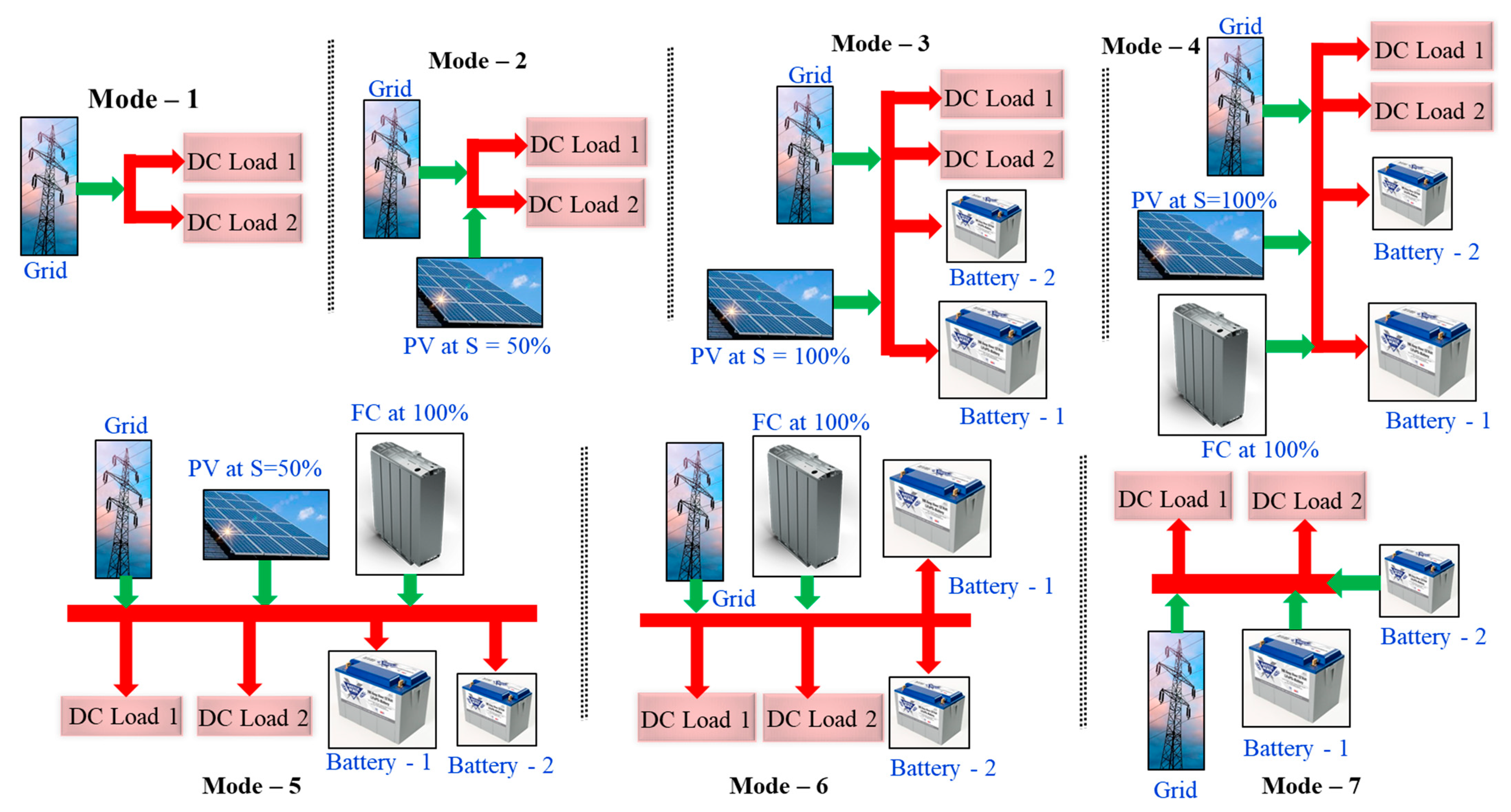
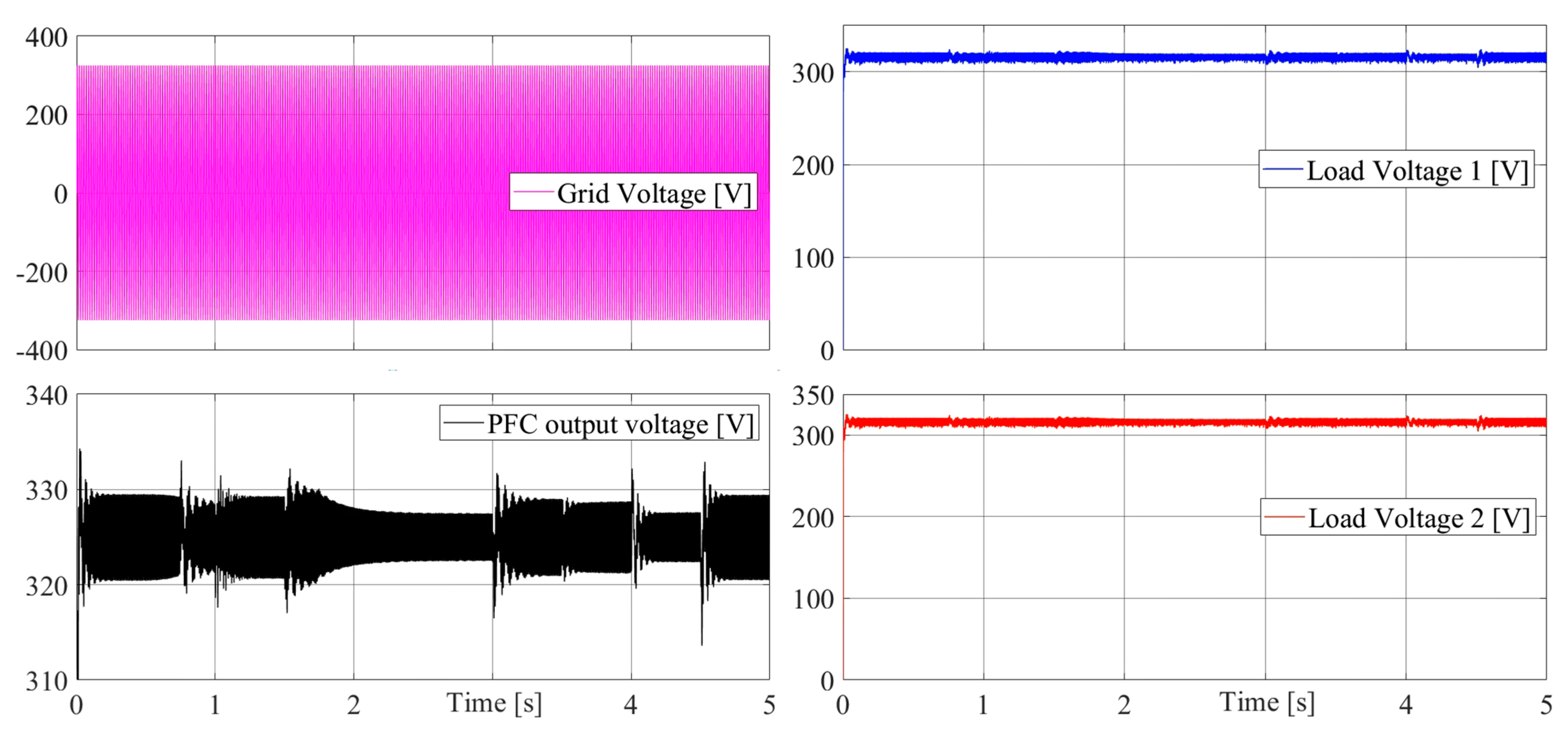
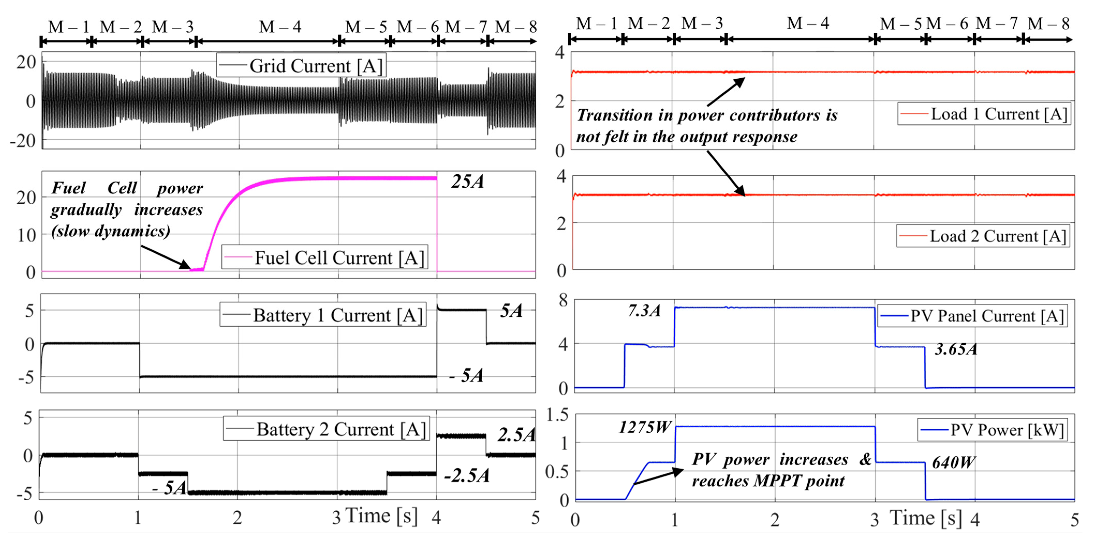
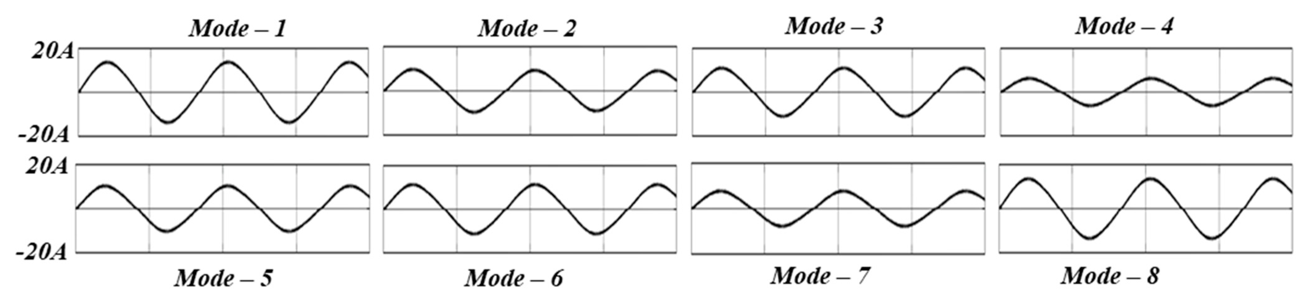
5. Simulation Results

To validate the performance of the proposed circuitry, simulation results are shown in Figure 5, (as per mode identification in Figure 4) where different operating modes are identified. The component specifications used for different circuits are given in Table 1 and Table 2. Figure 5 and Figure 6 show the simulation results from t = 0 to t = 5 s. Figure 7 shows a sinusoidal grid current for various modes of operation with unity power factor operation. In the discussion to follow, the focus is mainly on ensuring the optimum operation of the circuit along with the impact on the power drawn by the utility grid.
Mode–1: In this mode, the utility grid supplies power to dc loads. This mode is observed from t = 0 to t = 0.5 s. Here, the current drawn by the utility grid is observed to be perfectly sinusoidal, and unity power factor operation is ensured. This validates the optimum performance of the power factor correction circuit. During this mode, each secondary winding consumes approximately 1 kW (320 V, 100 Ω). The grid current has an rms value of 9.2 A and thus, the power drawn from the grid is 2116 W. The DC current at the input of the primary transformer winding is calculated to be 6.5 A. Thus, the circuit operates at an efficiency of 94.5%.
Mode–2: This mode is observed from t = 0.5 s to t = 1 s. At t = 0.5 s, the solar irradiation level of the PV panel increases from S = 0 to S = 500 W/m2. This invokes the MPPT algorithm, and the current supplied by the solar panel gradually moves towards the MPPT point (at the given insolation level) and finally settles there. Although the current can be observed to have reached the peak current value, the PV panel power rises slowly and reaches the MPPT point. This is the time required by the MPPT algorithm. During this mode, the PV panel supplies half of the rated current i.e., 3.65 A at approximately 640 W. This injection of power reduces the power and current drawn from the utility grid, as observed in Figure 5. At MPPT, the duty cycle of the boost converter is observed to be 0.54. Thus, the current pumped into the DAB converter primary winding by the PV panel is 1.97 A, which means that the input current of the DAB converter that is contributed by the utility grid decreases from 6.5 A to approximately 4.5 A (with the input grid current being 6.2 A rms).
Mode–3: This mode is observed from t = 1 s to t = 1.5 s. At t = 1 s, the solar irradiation level of the PV panel is increases from S = 0.5 kW/m2 to 1.0 kW/m2. With this increment in the solar irradiation level, the MPPT algorithm activates and shifts the operating point towards MPPT. During this mode, the power supplied by the solar panel is 1275 W at 7.3 A. As the power generated by the PV panel is at the rated value, Battery 1 and Battery 2, which are connected in the system, are charged at 5 A and 2.5 A, respectively. This means the power from the PV panel and the utility grid is used to feed dc loads and batteries. Compared to the previous mode, the addition of batteries charging the load compensates for the increase in PV power generation, and resultantly, the grid current that is drawn increases from 6.2 A (1.42 kW) to 7.3 A (1.68 kW).
Mode–4: This mode is observed from t = 1.5 s to t = 3 s. In this mode, the boost converter connected to the fuel cell is activated, and the converter is controlled to produce a 25 A current at the input of the boost converter. As fuel cell technology usually has higher current values at rated conditions, this converter demonstrates slow dynamics, and thus, this mode is observed for 1 s (compared to other modes demonstrated for 0.5 s).Controlling the fuel cell stack to inject 25 A at 45 V means the power supplied by the fuel cell is 1.125 kW. Due to this increase in generated power, the charging current of battery–2 incrases from 2.5 A to 5 A. This means the total power now supplied by the combination of the grid, PV panels, and fuel cell stacks are used to charge the two batteries and power the two dc loads. Due to the power contribution from the fuel cell stack, the current drawn by the utility grid reduces from 7.3 A (1.68 kW) to 4.1 A (940 W). This mode of operation exhibits the minimum amount power drawn by the utility grid. To further minimize the grid current, one of the battery charging loads can be disconnected. However, in the case of absolute zero grid current, the dc-link voltage available at the input of the triple-active half-bridge converter is not kept constant and is governed by the boost converters of the alternate energy sources. Thus, to maintain a fixed dc-link voltage, the grid current must be above minimum value throughout the operation.
Mode–5: This mode is observed from t = 3 s to t = 3.5 s. At t = 3 s, the solar irradiation level decreases from S = 1 kW/m2 to 0.5 kW/m2. This forces the MPPT algorithm to change the operating point to the MPPT condition at the given solar irradiation condition i.e., from 1275 W to 640 W (approx.). Even after this decrease in the PV panel contribution, the load on the system is kept constant. Due to this fall in PV power, the power drawn from the utility grid increases from 940 W (4.1 A) to 1.575 kW (6.9 A).
Mode–6: This mode is observed from t = 3.5 s to t = 4 s. At t = 3.5 s, and the PV panel experiences zero solar irradiation (emulating night condition). Due to this elimination of PV contribution, the current reference of Battery 2 is reduced from 5 A to 2.5 A. However, due to the absence of the PV contribution, the grid current now increases from 1.575 kW to approx. 1.8 kW (7.8 A). Conclusively, during this mode, the fuel cell stack and utility grid supply power to the batteries and dc loads.
Mode–7: This mode is observed from t = 4 s to t = 4.5 s. At t = 4 s, the power output of the fuel cell stacks reduces to zero. This power deficiency is now dealt with by changing the operating modes of the batteries from discharging to charging. Now Battery 1 and Battery 2 supply 5 A and 2.5 A (boost converter input currents) to the load. Thus, in this mode, both the batteries discharge in the load along with the utility grid with both the PV and the fuel cell stack generating zero power. During this mode, due to the battery contribution, the power drawn from the gird decreases from 1.8 kW to 1.35 kW.
Mode–8: The current contributions by the two batteries are now reduced to zero, and thus, this mode is similar to Mode–1. Here, the utility grid directly supplies the dc loads. Conclusively, it can be stated that successful integration and operation (at optimum conditions) are demonstrated here. Output voltages can then be used for powering the modules of the MMC converter.

6. Conclusions

This paper presents a novel multiport converter structure demonstrating that the easy integration of alternate energy sources can be achieved along with feeding isolated independent multiple loads. Solar PV panels, battery storage, and fuel cell stacks are easily integrated into the utility-powered system by using a modular converter structure. Additionally, the required isolation between the input and the output is achieved using a triple-active half-bridge converter, which allows independent power control of the connected dc loads. Simulation results were presented in detail verify the coordinated operation of various components to support system performance. To optimize the efficiency of the system, the power drawn by the utility grid is always real power due to the implementation of the power factor correction circuit, which achieves unity power factor operation.

Author Contributions

Writing—original draft preparation and methodology: S.R.; conceptualization, writing—review and editing, and supervision: I.K.; formal analysis and visualization: K.R.; review and funding: S.A.O.; review and editing: H.I.A.; methodology and funding: A.I. All authors have read and agreed to the published version of the manuscript.

Funding

This research was funded by Taif University Researchers Supporting Project, number (TURSP-2020/228).

Conflicts of Interest

The authors declare no conflict of interest.

References

  1. Rodríguez, J.; Bernet, S.; Wu, B.; Pontt, J.O.; Kouro, S. Multilevel voltage-source-converter topologies for industrial medium-voltage drives. IEEE Trans. Ind. Electron. 2007, 54, 2930–2945. [Google Scholar] [CrossRef]
  2. Abu-Rub, H.; Holtz, J.; Rodriguez, J.; Baoming, G. Medium-voltage multilevel converters—State of the art, challenges, and requirements in industrial applications. IEEE Trans. Ind. Electron. 2010, 57, 2581–2596. [Google Scholar] [CrossRef]
  3. Rahman, S.; Meraj, M.; Iqbal, A.; Tariq, M.; Maswood, A.I.; Ben-Brahim, L.; Al-ammari, R. Design and Implementation of Cascaded Multilevel qZSI Powered Single-Phase Induction Motor for Isolated Grid Water Pump Application. IEEE Trans. Ind. Appl. 2019, 56, 1907–1917. [Google Scholar] [CrossRef]
  4. Lai, J.-S.; Peng, F.Z. Multilevel converters—A new breed of power converters. IEEE Trans. Ind. Appl. 1996, 32, 509–517. [Google Scholar]
  5. Kazmierkowski, M.P.; Franquelo, L.G.; Rodriguez, J.; Perez, M.A.; Leon, J.I. High-performance motor drives. IEEE Ind. Electron. Mag. 2011, 5, 6–26. [Google Scholar] [CrossRef] [Green Version]
  6. Akagi, H. Multilevel converters: Fundamental circuits and systems. Proc. IEEE 2017, 105, 2048–2065. [Google Scholar] [CrossRef]
  7. Rashid, M.H. Power Electronics Handbook; Butterworth-Heinemann: Oxford, UK, 2017; ISBN 0128114088. [Google Scholar]
  8. Khan, F.H.; Tolbert, L.M. A multilevel modular capacitor-clamped DC–DC converter. IEEE Trans. Ind. Appl. 2007, 43, 1628–1638. [Google Scholar] [CrossRef]
  9. Priya, M.; Ponnambalam, P.; Muralikumar, K. Modular-multilevel converter topologies and applications—A review. IET Power Electron. 2019, 12, 170–183. [Google Scholar] [CrossRef]
  10. Rohner, S.; Bernet, S.; Hiller, M.; Sommer, R. Modulation, losses, and semiconductor requirements of modular multilevel converters. IEEE Trans. Ind. Electron. 2009, 57, 2633–2642. [Google Scholar] [CrossRef]
  11. Kumar, A.; Wang, Y.; Raghuram, M.; Pilli, N.K.; Singh, S.K.; Pan, X.; Xiong, X. A Generalized Switched Inductor Cell Modular Multilevel Inverter. IEEE Trans. Ind. Appl. 2019, 56, 507–518. [Google Scholar] [CrossRef]
  12. Bina, M.T. A transformerless medium-voltage STATCOM topology based on extended modular multilevel converters. IEEE Trans. Power Electron. 2010, 26, 1534–1545. [Google Scholar]
  13. Marzoughi, A.; Burgos, R.; Boroyevich, D. Optimum design guidelines for the modular multilevel converter in active front-end applications: Considerations for passive component reduction. IEEE Power Electron. Mag. 2018, 5, 56–65. [Google Scholar] [CrossRef]
  14. Sharifabadi, K.; Harnefors, L.; Nee, H.-P.; Norrga, S.; Teodorescu, R. Design, Control, and Application of Modular Multilevel Converters for HVDC Transmission Systems; John Wiley & Sons: Hoboken, NJ, USA, 2016; ISBN 1118851560. [Google Scholar]
  15. Zeng, R.; Zhao, B.; Wei, T.; Xu, C.; Chen, Z.; Liu, J.; Zhou, W.; Song, Q.; Yu, Z. Integrated gate commutated thyristor-based modular multilevel converters: A promising solution for high-voltage dc applications. IEEE Ind. Electron. Mag. 2019, 13, 4–16. [Google Scholar] [CrossRef]
  16. Debnath, S.; Qin, J.; Bahrani, B.; Saeedifard, M.; Barbosa, P. Operation, control, and applications of the modular multilevel converter: A review. IEEE Trans. Power Electron. 2014, 30, 37–53. [Google Scholar] [CrossRef]
  17. Raju, M.N.; Sreedevi, J.; Mandi, R.; Meera, K.S. Modular multilevel converters technology: A comprehensive study on its topologies, modelling, control and applications. IET Power Electron. 2019, 12, 149–169. [Google Scholar] [CrossRef]
  18. Lachichi, A.; Junyent-Ferre, A.; Green, T. Optimal design of a LCL filter for LV modular multilevel converters in hybrid AC/DC microgrids application. In Proceedings of the IECON 2018—44th Annual Conference of the IEEE Industrial Electronics Society, Washington, DC, USA, 21–23 October 2018; pp. 3973–3978. [Google Scholar]
  19. Lachichi, A.; Junyent-Ferre, A.; Green, T.C. Comparative optimization design of a modular multilevel converter tapping cells and a 2L-VSC for hybrid LV ac/dc microgrids. IEEE Trans. Ind. Appl. 2019, 55, 3228–3240. [Google Scholar] [CrossRef]
  20. Akagi, H. Classification, terminology, and application of the modular multilevel cascade converter (MMCC). IEEE Trans. Power Electron. 2011, 26, 3119–3130. [Google Scholar] [CrossRef]
  21. Wu, M.; Li, Y.W.; Konstantinou, G. A Comprehensive Review of Capacitor Voltage Balancing Strategies for Multilevel Converters Under Selective Harmonic Elimination PWM. IEEE Trans. Power Electron. 2020, 36, 2748–2767. [Google Scholar] [CrossRef]
  22. Ronanki, D.; Williamson, S.S. Modular multilevel converters for transportation electrification: Challenges and opportunities. IEEE Trans. Transp. Electrif. 2018, 4, 399–407. [Google Scholar] [CrossRef]
  23. Tang, Y.; Ran, L.; Alatise, O.; Mawby, P. Capacitor selection for modular multilevel converter. IEEE Trans. Ind. Appl. 2016, 52, 3279–3293. [Google Scholar] [CrossRef]
  24. Wang, S.; Liu, T.; Huang, X.; Yu, Y. Capacitor voltage balancing control with reducing the average switching frequency in MMC. J. Eng. 2019, 2019, 2375–2380. [Google Scholar] [CrossRef]
  25. Zhang, Y.; Adam, G.P.; Lim, T.C.; Finney, S.J.; Williams, B.W. Analysis of modular multilevel converter capacitor voltage balancing based on phase voltage redundant states. IET Power Electron. 2012, 5, 726–738. [Google Scholar] [CrossRef]
  26. Gao, C.; Liu, X.; Liu, J.; Guo, Y.; Chen, Z. Multilevel converter with capacitor voltage actively balanced using reduced number of voltage sensors for high power applications. IET Power Electron. 2016, 9, 1462–1473. [Google Scholar] [CrossRef]
  27. Dekka, A.; Wu, B.; Zargari, N.R. A novel modulation scheme and voltage balancing algorithm for modular multilevel converter. IEEE Trans. Ind. Appl. 2015, 52, 432–443. [Google Scholar] [CrossRef]
  28. Zhao, B.; Song, Q.; Liu, W.; Sun, Y. Overview of dual-active-bridge isolated bidirectional DC–DC converter for high-frequency-link power-conversion system. IEEE Trans. Power Electron. 2013, 29, 4091–4106. [Google Scholar] [CrossRef]
  29. Tao, H.; Kotsopoulos, A.; Duarte, J.L.; Hendrix, M.A.M. Family of multiport bidirectional DC–DC converters. IEE Proc. -Electr. Power Appl. 2006, 153, 451–458. [Google Scholar] [CrossRef] [Green Version]
  30. Zhao, W.; Zhang, X.; Gao, S.; Ma, M. Improved Model-Based Phase-Shift Control for Fast Dynamic Response of Dual Active Bridge DC/DC Converters. IEEE J. Emerg. Sel. Top. Power Electron. 2020, 9, 223–231. [Google Scholar] [CrossRef]
  31. Bu, Q.; Wen, H.; Wen, J.; Hu, Y.; Du, Y. Transient DC Bias Elimination of Dual Active Bridge DC-DC Converter with Improved Triple-Phase-Shift Control. IEEE Trans. Ind. Electron. 2019, 67, 8587–8598. [Google Scholar] [CrossRef]
  32. Naayagi, R.T.; Forsyth, A.J.; Shuttleworth, R. High-power bidirectional DC–DC converter for aerospace applications. IEEE Trans. Power Electron. 2012, 27, 4366–4379. [Google Scholar] [CrossRef]
  33. Naayagi, R.T.; Forsyth, A.J.; Shuttleworth, R. Bidirectional control of a dual active bridge DC–DC converter for aerospace applications. IET Power Electron. 2012, 5, 1104–1118. [Google Scholar] [CrossRef]
  34. 95% Efficiency, 1-kW Analog Control AC/DC Reference Design for 5G Telecom Rectifier. Available online: https://www.ti.com/lit/ug/tiduet4a/tiduet4a.pdf?ts=1627097917458&ref_url=https%253A%252F%252Fwww.google.com.hk%252F (accessed on 24 June 2021).
  35. Texas Instruments. Bi-Directional, Dual Active Bridge Reference Design for Level 3 Electric Vehicle Charging Stations; Texas Instruments: Dallas, TX, USA, 2019; pp. 1–51. [Google Scholar]
  36. Dung, N.A.; Chiu, H.-J.; Lin, J.-Y.; Hsieh, Y.-C.; Liu, Y.-C. Efficiency optimisation of ZVS isolated bidirectional DAB converters. IET Power Electron. 2018, 11, 1499–1506. [Google Scholar] [CrossRef]
  37. Hauke, B. Basic Calculation of a Boost Converter’s Power Stage; Application Report; Texas Instruments: Dallas, TX, USA, 2009; pp. 1–9. [Google Scholar]
Figure 1. Block diagram of the proposed system.
Electronics 10 01779 g001
Figure 2. Detailed circuit diagram of the integrated converter.
Electronics 10 01779 g002
Figure 3. Primary control algorithms for different components of the system.
Electronics 10 01779 g003
Figure 4. Different modes of operation possible with the interconnected components with the aim of minimizing power drawn from utility grid (FC = Fuel Cell).
Electronics 10 01779 g004
Figure 5. Voltages observed at different points in the system—input grid voltage, power factor correction (PFC) circuit output voltage and load voltages measured at the two outputs of the DAB converters.
Electronics 10 01779 g005
Figure 6. Current supplied and drawn by various components of the integrated system.
Electronics 10 01779 g006
Figure 7. Grid current during all the modes exhibiting sinusoidal waveshape thereby mnimizing harmonics.
Electronics 10 01779 g007
Table 1. Component specification of PV panel, fuel cell stacks, and battery specifications.
ParameterSpecificationParameterSpecificationParameterSpecification
Total solar rating 1275 WFuel Cell SpecificationsBattery 1 Specifications
Part Number1STH-215-PNominal current 35 ABattery Rating160 V, 10 A
MPPT point213 W, 29 V, 7.35 A Nominal voltage45 V Series Inductor4 mH, 15 A
Open circuit voltage36.3 VMaximum current70 AFiltering capacitor100 µF, 600 V
Short circuit current7.84 AMaximum voltage37 VBattery 2 Specifications
Configuration6 Series panelsEfficeincy of Fuel
Cell Stcik (ηstack)
55%Battery rating80 V, 10 A
Series Inductor2 mH, 10 ASeries Inductor3 mH, 15 A
Output capacitor100 µF, 600 VSeries Inductor1 mH, 50 AFiltering capacitor100 µF, 600 V
Input capacitor 2.5 mF, 300 VFiltering capacitor150 µF, 600 VInitial SOC80%
Boost switch600 V, 10 ABoost switch rating600 V, 50 ABoost switch rating 600 V, 15 A
Series diode 600 V, 10 ASeries diode rating600 V, 50 ASeries switch rating600 V, 15 A
Table 2. Component specifications of power factor correction circuit and dual active half bridge converter.
ParameterSpecificationParameterSpecificationParameterSpecification
Diode Bridge Rectifier + PFCDAB Converter SpecificationsTransformer Specification
Diode Rating 600 V, 20 A (General)Switches600 V, 10 APower rating 2 kW
Boost switch600 V, 20 A Capacitors 20 µF, 600 VVoltage rating230 V (rms)
Series diode600 V, 20 A (fast recovery) Load100 ΩSwitching frequency 40 kHz
Series inductor 5 mH, 20 ATurns’ ratio-1 1:1Maximum phase shift6.25 us
Output capacitor1.5 mF, 600 VTurns’ ratio-2 1:1Leakage inductance 12 uH, 0.02 Ω
Publisher’s Note: MDPI stays neutral with regard to jurisdictional claims in published maps and institutional affiliations.

