
A Hybrid Control Scheme with Fast Transient and Low Harmonic for Boost PFC Converter


1
Department of Electrical Engineering, National Formosa University, No. 64, Wunhua Rd., Huwei Township, Yunlin County 632, Taiwan
2
Aplustek Integrated Circuits Corp, National Formosa University, No. 372, Minsheng Rd., Taoyuan Dist., Taoyuan City 330, Taiwan
3
Department of Vehicle Engineer, National Formosa University, No. 64, Wunhua Rd., Huwei Township, Yunlin County 632, Taiwan
*
Author to whom correspondence should be addressed.
Electronics 2021, 10(15), 1848; https://0-doi-org.brum.beds.ac.uk/10.3390/electronics10151848
Submission received: 2 July 2021
/
Revised: 28 July 2021
/
Accepted: 29 July 2021
/
Published: 31 July 2021
(This article belongs to the Special Issue Automotive Electronics)
Abstract
:In this study, a new control strategy was proposed to improve transient response and the input current harmonic distortion of power factor correction (PFC) regulators operating in an average current mode. The proposed technique required only two additional gain selectors and a peak detector circuit on the feedforward voltage loop and output voltage feedback loops. It provided a direct reading for the average voltage value of feedback control loops and the peak voltage of feedforward control loops, producing PFC boost regulators with fast dynamic responses and low-input current harmonic distortion. The use of digital potentiometers for directly changing the gain of control loops did not require any divider or squarer to reduce the complexity of control circuits. The operating principles and control strategies of 300 W boost PFC with the new control strategy are presented with detailed analysis and discussion. The experimental results were satisfactory.
1. Introduction
Currently, mainstream power supplies on the market are designed and developed using high-frequency switching technologies to achieve compactness and high performance. However, power switching is affected by nonlinear resistance, which leads to harmonic pollution of electrical devices and even increases the loss of transmission lines [1]. Therefore, the International Electrotechnical Commission (IEC) stipulated relevant standards for power harmonics such as the IEC 61000-3-2 standard [2].
In order for the problem of harmonic pollution to be solved, the active power factor correction (PFC) technique is the most suitable method because it increases the input power factor (PF) and reduces input current harmonic distortion [3]. Common current mode control methods include peak current control and average current control methods. Because the peak current control method is likely to be affected by noise [4] and requires slope compensation [5], the average current control method is extensively applied in switching power supply industries. As shown in Figure 1, the average current control method features current and voltage control loops [6,7]. The current control loop controls the phase difference between input current and voltages, whereas the voltage control loop regulates the direct current (DC) output voltage. Both control loops contain twice-line frequency ripples; therefore, the input currents generate second harmonic distortion. The increase in the ripple voltage increases input current harmonic distortion (total harmonic distortion; THDi). Commonly, to reduce the second harmonic effect, the voltage and current loop bandwidth are limited. However, this design drags the system transient response. In applications for light-emitting diode drivers or adapters, fast dynamic responses must be considered because, when load currents change, the output voltage frequently generates oscillation.
To achieve THDi with a fast dynamic response and reduced input current, researchers have proposed many methods [8,9,10,11,12,13,14]. Studies [8,9,10] have adopted a two-stage scheme, with the front-end and back-end schemes serving to reduce THDi and improve transient responses, respectively. In addition, increasing additional circuits in the control loop is an effective improvement method. For example, the studies [11,12,13] used a sample-and-hold (S/H) circuit to sample output feedback voltage at the zero crossing point of input voltage. Digital control technologies are other common solutions [5,14,15,16,17] because digital controllers have the advantages of accurate time control and easily increased system flexibility. For example, the average sliding control technique can be used to determine the relationship between the sliding surface and the input voltage and current and to further reduce input current harmonics [17,18,19,20]. The digital signal processors can be used as the control core and combined with the reference commands provided by phase-locked loops to avoid voltage loops from being affected by twice-line frequency. Subsequently, the voltage loop bandwidth can be increased, and PFC transient responses improved [21].
The described methods can prevent voltage loops from being affected by twice-line frequency and increase voltage loop bandwidths, addressing the defects of conventional techniques. However, the complexity of the controllers will increase, and complex algorithms and high-cost microcontrollers are required.
Moreover, one cycle control method is also a novel technique. It does not need a multiplier and the rectifying signal from input voltage; consequently, high power factor can be achieved easier with fewer components. This method will not be influenced by 120 Hz ripple from the rectified input voltage, and this benefit helps PFC to operate in wider range of the bandwidth. However, this technique requires a resettable integrator and a comparator. The switching noise will be a major concern and impact for the comparator [22].
Therefore, in this study, a new control technique was proposed that requires only two additional digital potentiometers, two analog-to-digital converters (ADCs), and a zero-point detection circuit. When the zero-point detection circuit detected input voltage zero points, ADCs are employed to sample input voltage peaks and feedback error signals. The sampling results inform the adjustment of digital circuits to change the system loop gains and complete PFC operations. This prevents the system from being affected by twice-line frequency ripples and subsequently increased the system bandwidths. In this system, the controller requires no dividers or squarer, thereby reducing the overall circuit complexity.
This paper comprises six sections. Section 2 illustrates the operating principles. Section 3 explains the control circuit design. Section 4 describes the stability analysis and compensator design. Section 5 provides the experimental results, which were verified for the 300 W boost power PFC prototype. Section 6 provides the conclusions of this study.
2. Description of the Proposed Scheme
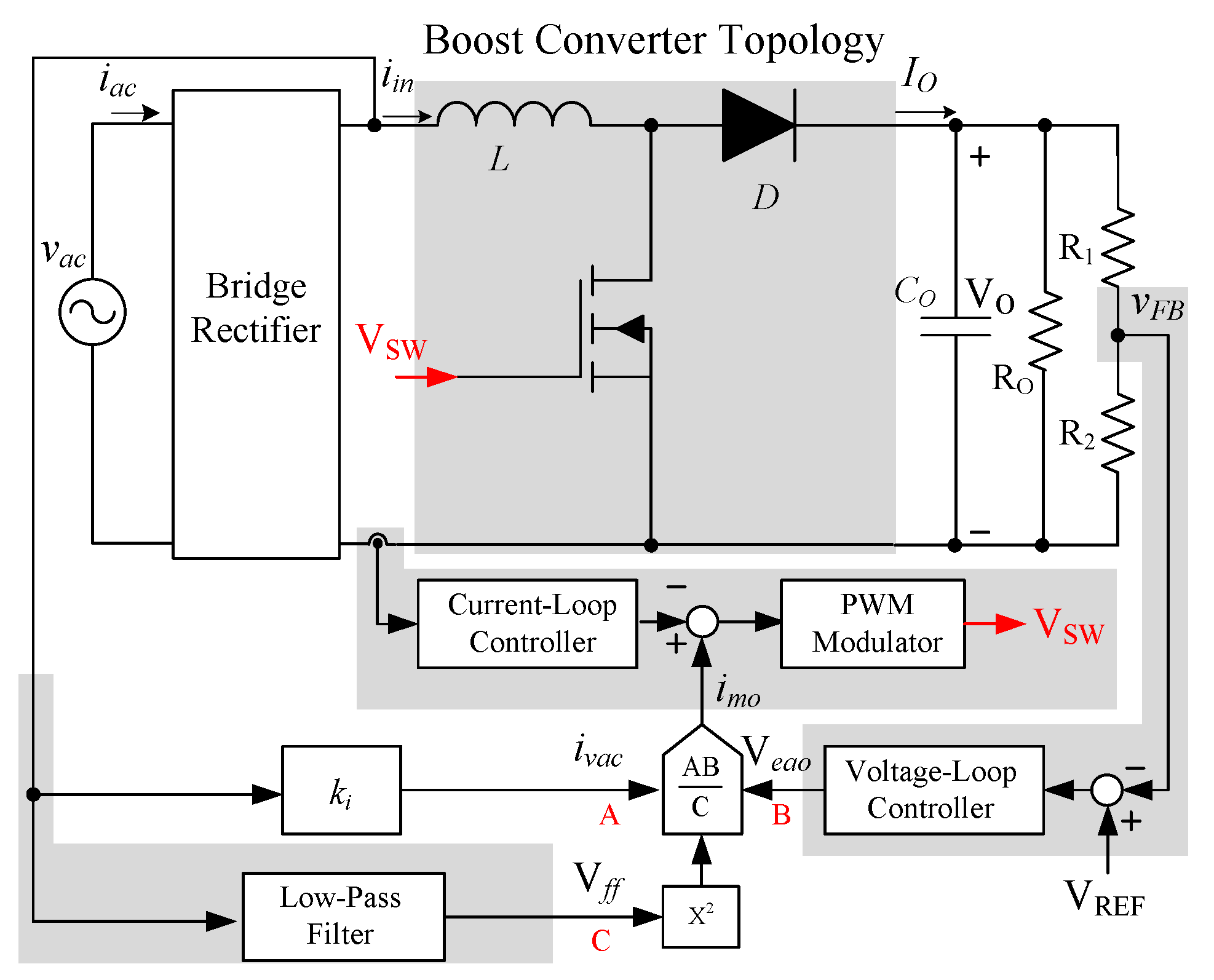
Figure 1 shows the control circuit block diagram conventionally operating in the average current mode. In the circuit scheme, the boost converter is adopted. In terms of the simplification of the analysis, all components are assumed to be ideal. The current command imo decides the waveform of the input current iin, which is composed of three main parameters, namely, rectified input current ivac, feedforward voltage vFF, and feedback voltage Veao. In a steady state, the current control command imo can be expressed as follows:
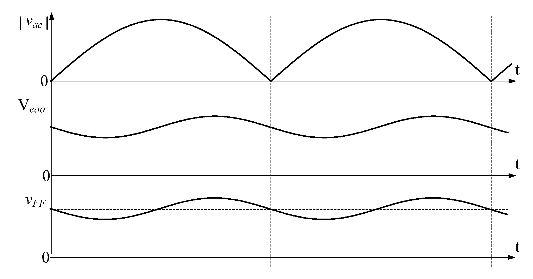
The input voltage is a sinusoidal wave rectified through a bridge full-wave rectifier, and filter capacitors are added at the feedforward loop; therefore, Veao and vFF simultaneously feature DC and low-frequency 120 Hz alternating current (AC) components, as shown in Figure 2 [21]. To avoid PFC-induced input current harmonic distortion, the conventional method uses narrow bandwidth filters to inhibit low-frequency components; however, the PFC transient response speed is limited.
Figure 2 shows that, when the input voltage vac is at the peak or zero point, the values for the voltage error signal Veao and the voltage feedforward signal vFF are their respective means. Therefore, the input voltage peak and feedforward means are proportionally related. When the input voltage peak increases, the feedforward signal means increase. Conversely, when the input voltage peak decreases, the feedforward signal means decrease. In summary, the feedforward loops in this study use no filter capacitors; instead, they use peak detectors to read the feedforward signal peak voltage as the feedforward command vFF to improve the input transient responses. For the output feedback, a 120 Hz S/H device is employed to sample the voltage error signal Veao. This method maintains the signal Veao at the mean value between sample intervals.
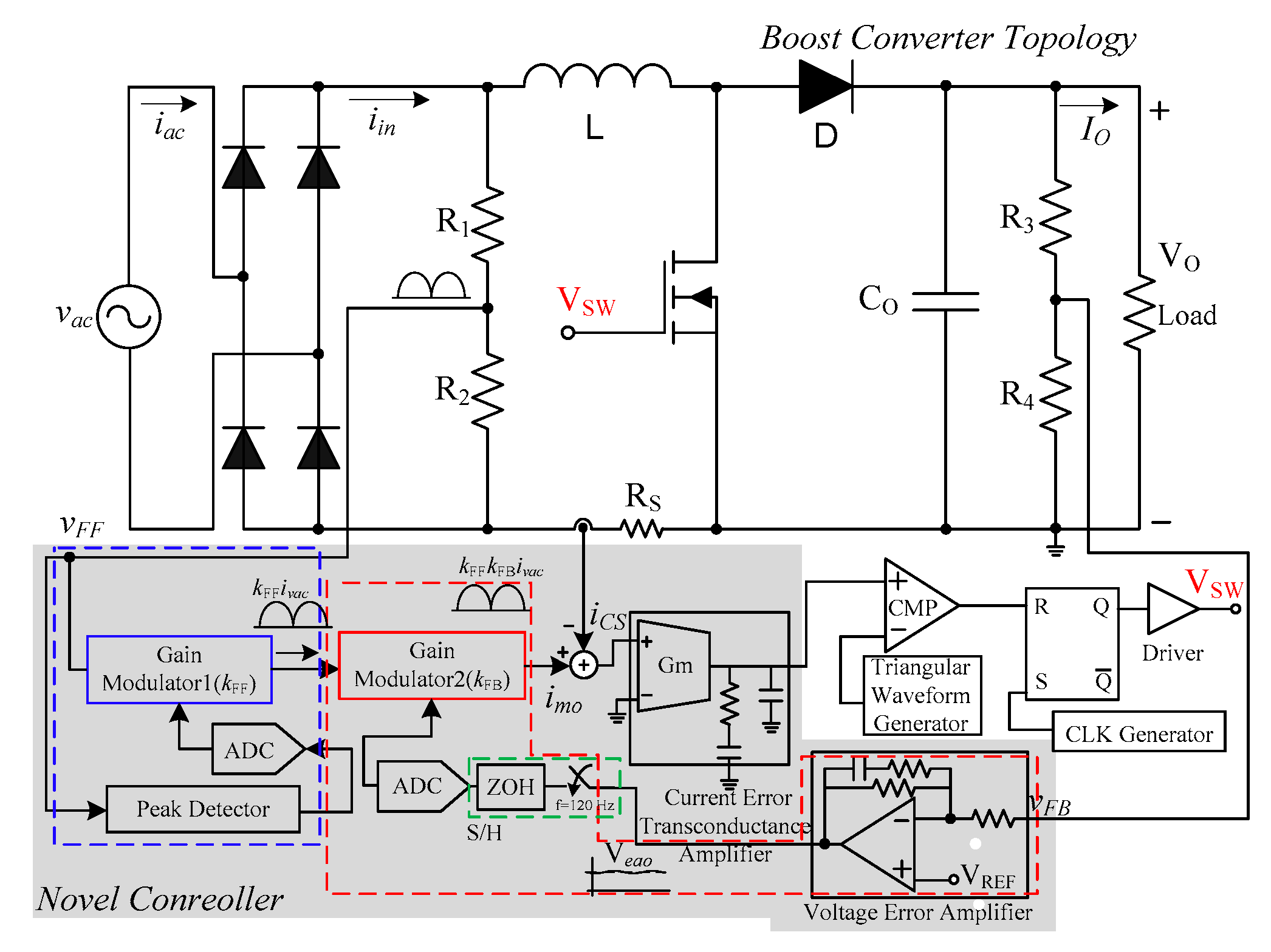
A new control scheme was proposed, as shown in Figure 3, with two gain control circuits (kFF, kFB), two ADCs, a peak detector, a transconductance amplifier, and an S/H circuit. The core of the controller consists of two adjustable gain modulators, which are separately located at the feedforward loop (dotted blue line) and the voltage feedback loop (dotted red line). On the feedforward loop, the voltage vFF is generated by the input voltage vac through a bridge rectifier. Peak detectors sample voltage vFF results to adjust the gain kFF size. In addition, to eliminate the effect of output voltage ripples on voltage feedback loops, the error signals Veao for controlling the gain kFB size are determined by the S/H circuit with a 120-Hz sampling frequency and an ADC. Through the aforementioned analysis, the input current reference command imo can be rewritten as follows:
where kFF(k) and kFB(k) are respectively the kth feedforward gain and feedback gain. The comparison results of (1) and (2) reveal that, when and , the size of the two gains can be adequately adjusted for PFC control.
According to (2), the current control command is determined by the output of the rectified line voltage peak and the voltage error amplifier. Therefore, the command can simultaneously control the converter input impedance, demonstrating resistance and stable output voltage. Subsequently, the roles of the gains kFF(k) and kFB(k) in this study are explained.
The gain kFF(k) provides an open-loop modification that maintains voltage loop gain at a constant value. For example, when the output power remains unchanged (fixed kFB) and the input voltage doubles, the peak detector readjusts the gain controller size as follows:
The results reveal that, although the current ivac is doubled, the current command imo(t) is halved, maintaining input power identical to that in the previous state.
The gain kFB(k) is controlled using the voltage error amplifier. When the output power increases, the output voltage Veao of the voltage error amplifier increases. Through the digital output of the ADC, the gain kFB(k) is increased to change the value of the root mean square of the current command imo(t) to stabilize the output voltage. By contrast, when the output power decreases, the gain kFB(k) decreases the root mean square value of the current command imo(t). Notably, on the basis of the twice-line frequency, sampling of the S/H circuit is conducted to obtain a point within a half-wave cycle of the supply mains to ensure that the gain kFB(k) is unaffected by the 120 Hz output ripple voltage.
3. Control Circuit
3.1. Feedforward Loop Control Circuit
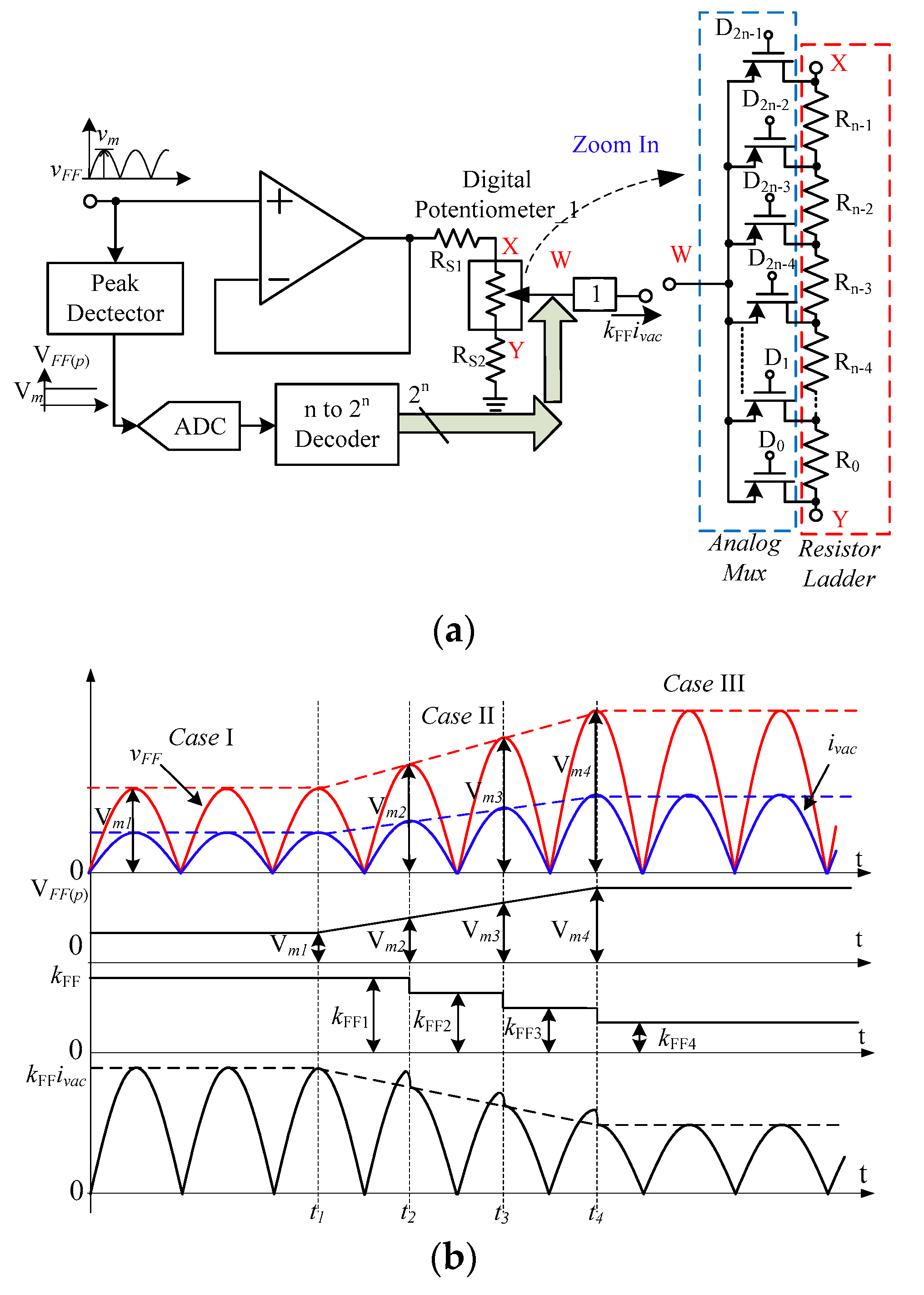
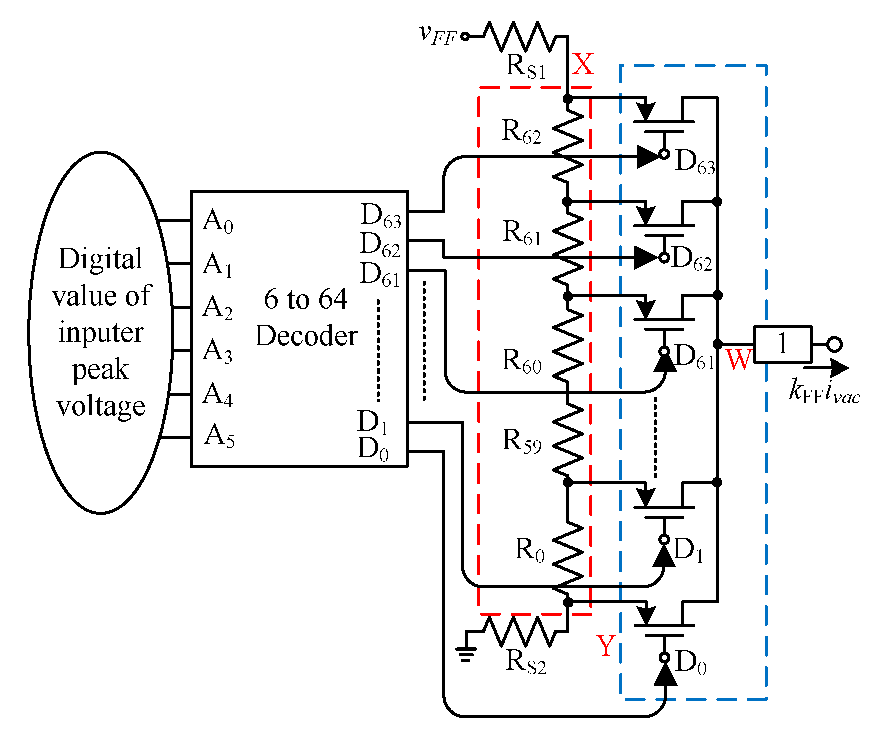
Figure 4a shows the feedforward loop control circuit scheme of the proposed new control strategy, which uses digital potentiometers and an operational amplifier to adjust the kFF. The digital potentiometers play key roles in the circuits because they adjust the command of the gain kFF according to the feedforward voltage vFF peak. General digital potentiometers comprise resistor ladder and wiper. The resistor ladder is composed of equivalent series resistances, and the wiper uses digital signals to control the conduction of analog switches and set series resistance [23].
The square of feedforward voltage vFF is used to determine the gain kFF; therefore, the resistor ladder of the first digital potentiometer is not composed of equivalent series resistance but has an appropriate design. Figure 4b illustrates the process of feedforward control circuit adjustment for kFF when the input voltage varies. Next, Figure 4a,b illustrates Case I, Case II, and Case III to demonstrate the operating principles of the feedforward loop control circuit. To simplify the analysis of operating principles, all components are assumed to be ideal:
Case I:
In this interval, the peak detectors begin to sample the voltage peak for vFF as shown in Figure 4b. When the voltage peak Vm1 is determined, the ADC converts analog signals into a certain proportion of digital signals. The n-bit decoder is then used to generate D(0) to D(2n−1) outputs to set the wiper and adjust the resistance value to determine the size of the gain kFF. The gain kFF is calculated using the following equation.
where and respectively represent the sums of series resistance between terminals W and X and between terminals W and Y. Equation (4) indicates that the gain kFF contains no 120-Hz ripple component subject to steady-state operation; accordingly, the input current harmonic distortion can be reduced.
Case II:
This interval is the transient region (t1–t4) of input voltage variation, as shown in Figure 4b. At t1, the voltage peak begins to increase from Vm1 to Vm4, and the peak detector output voltage increases accordingly. According to the ADC output value, the decoder then controls the analog switch of the digital potentiometer to move terminal W toward terminal Y, thereby completing the operation of reducing gain kFF. Notably, the ADC samples only at t2, t3, and t4. Therefore, the gain kFF changes once in a cycle (8.33 ms). For example, in the interval , the peak detector output voltage increases with time, but the gain kFF only changes from kFF1 to kFF2.
Case III:
At t4, the output voltage again reaches a steady state, and the input voltage peak remains identical. The digital potentiometer maintains the feedforward gain kFF4 according to the ADC digital data, as shown in Figure 4b. Although the input voltage varies with time, the proposed control strategy enables the feedforward loop gain to be maintained at a fixed value, simplifying the design of the loop compensator.
The analysis results indicate the role of gain kFF in PFC feedforward loop control. Subsequently, the design for gain kFF is described. The general grid specification is between 90 and 265 Vrms. For the facilitation of the PFC operation in the specification, the gain kFF is designed accordingly. First, the resolution of the digital potentiometer is considered. Higher resolution increases the accuracy of signals. However, each piece of data requires increasing numbers of bits, and the ADC price increases.
In this study, the ADC is only required to sample the input peak voltage; thus, the resolution has the minimum bit requirement, which can be expressed using the following equation:
where and respectively represent the maximum input voltage peak and minimum voltage peak. For the proposed specification, the maximum input voltage peak was 375 V, and the minimum resolution unit was 4 V. Equation (5) can be used to determine the resolution bit for . A 6-bit resolution ADC and a digital potentiometer with 6-bit resolution are adopted to satisfy the varying input voltage peaks corresponding to various gain kFF sizes.
Equation (2) indicates that, in fixed output power conditions, the current command can be determined through kFFivac. Figure 5 shows the proposed feedforward loop circuit scheme, which uses a 6-to-64 line decoder to decode input voltage peak results and control the conduction position of analog switches, thereby changing the current command size. Table 1 shows the truth table of the 6-to-64 line decoder corresponding to input peak voltage. When the input peak voltage VFF(p) = VmB is decoded as ((B)10 = (A5A4A3A2A1A0)2), D(B) = 1 is output to drive conduction of the analog switch. The current command kFFivac can be expressed as follows:
where B is a constant ranging from 1 to 63.
In particular, when B = 0, the current command can be expressed as follows:
3.2. Voltage Feedback Loop Control Circuit
The main function of the voltage feedback loop is to regulate PFC and maintain a stable output voltage. In the conventional design method, the rectified input voltage is multiplied by the voltage error signal Veao and the product divided by squared feedforward voltage vFF. Subsequently, a current control command imo is generated to regulate the input current size and achieve stable output voltage control. As such, the voltage Veao and current control command imo are in direct proportional relationship. Moreover, the bandwidth of voltage loops must be set far lower than that of the input line voltage because excessively wide bandwidth may cause severe input current harmonic distortion [24]. Therefore, the conventional method cannot simultaneously improve the voltage transient response and input current harmonic distortion.
To improve the shortcoming of the conventional PFC control strategy caused by the voltage loop, we adopted a digital potentiometer, an ADC, and an S/H circuit in the voltage loop, as shown in Figure 6a. When the input load varies, the voltage feedback control circuit adjusts kFB through the process in Figure 6b. To simplify the analysis of operating principles, we assumed all components to be ideal.
State 1 (t0–t1):
Before t1, PFC is performed at a steady state. The second digital potentiometer adjusts the wiper W to a suitable position according to the Veao decoded using the ADC, as shown in Figure 6b. Because the ADC sampling time is determined by the twice-line frequency, PFC can avoid from the effect of voltage Veao ripples.
According to Figure 6a, the resistor ladder structure of the second digital potentiometer is different from that of the first. It is composed of equivalent series resistance RS, where a total of 2n series resistances is observed between terminal X and terminal Y. The wiper of the second potentiometer has identical functions to that of the first, namely, to set any of the 2n − 1 resistances through conduction of the analog switch.
Because the terminals X and Y of the digital potentiometer are respectively connected to the feedforward loop control command signal kFFivac and the operational amplifier output end, the circuit output is expressed as follows:
where
Equation (8) indicates that the adjustment of gain can facilitate a proportional relationship between voltage Veao and current control command imo without any 120 Hz ripple component in kFB.
State 2 (t1~t4):
When the PFC output load is instantaneously switched from a light load (10%) to a heavy load (100%), the potential of the output voltage decreases suddenly, as shown in the dotted red line in Figure 6b. The error amplifier then compares the feedback voltage vFB and reference voltage VREF to obtain the required error signal Veao. Through the error signal, the wiper of the potentiometer is adjusted to increase kFB, thereby facilitating the rapid restoration of PFC output voltage from a lower value to the normal voltage range. Consequently, the goal of stable output voltage is achieved, as shown in Figure 6a.
In this state, although ADC sampling is conducted only at t2, t3, and t4, the voltage loop bandwidth—without the effect of the output voltage ripple—can be set at a larger value compared with for the conventional method.
In addition, the output power specification must be considered in the resolution of the second digital potentiometer. Theoretically, higher ADC resolutions entail more accurate sampling results for the output power. However, due to cost limits, this study used 2% output power as the minimum resolution unit. The minimum resolution bit can be determined using (9):
where is the maximum output power. This study set a specification of 300 W for the maximum output power. Equation (9) indicates that the ADC resolution and the resolution of the second digital potentiometer must be 6 bits. The ADCs with 50-kHz sampling frequencies are currently common on the market. This sampling frequency is enough to increase voltage loop bandwidth. Thus, this study adopted the ADC with said sampling frequency.
Table 2 provides a comparison between the predictive CCM average current control technique and the proposed technique. It is worth noticing that the predictive CCM average current control technique performs better, but it requires a DSP to achieve the algorithm. This is much more complex, and the cost of circuit is higher. In this paper, the proposed control technique can be integrated as an IC by using the ADC and the digital potential meter structure. The cost is much lower than the control technique with DSP controller.
4. Design Criteria
Two adjustable gain modulators are used to resolve the defects of poor conventional PFC transient response. Therefore, the settings of the two digital variable resistances are critical. The selection of a compensator, digital potentiometer resolution, and gain range require consideration as well as the inductors, power switch, and diode voltage and current-withstand capacities. For the proposed PFC, we applied the following circuit parameter settings.
- Input AC voltage: vac = 110 Vrms~220 Vrms;
- Output DC voltage: VO = 385 VDC;
- Output maximum power: PO(max) = 300 W;
- Switching frequency: fS = 70 kHZ.
4.1. Digital Potentiometer
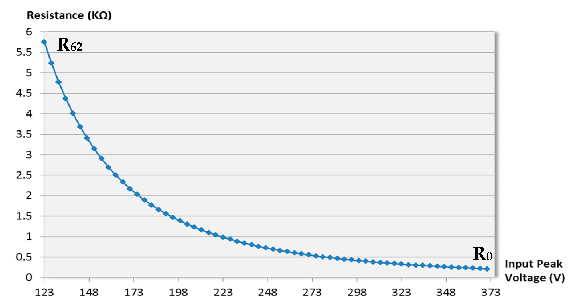
In (6), the current command kFFivac and feedforward voltage vFF are crucial parameters for determining the series resistance of the first digital potentiometer. If maximum output power is set as a condition, when the input voltage reaches the maximum peak, the feedforward voltage vFF maximum peak is Vm(max). Table 1 indicates that, D0 = 1 for the decoder when the voltage peak is at its maximum. The minimum peak of the current command kFFivac can be predicted because its peak value depends on the input current. The relationship for resistance RS2 can be expressed as follows:
By contrast, when the feedforward voltage vFF is at the minimum peak Vm(min), the decoder D63 = 1. The relationship for resistance RS1 is expressed as follows:
Reorganization of (10) and (11) yields the following relationship between the resistances RS2 and RS1:
Per the aforementioned specification, the maximum peak range of the input current is between 1.60 and 4.88 A. Therefore, the current command A and A. Vm(max) = 15 V and Vm(min) = 4.92 V. Equation (11) yields the resistance RS2 = 10 k Ω and RS1 = 827 Ω. In summary, the resistance of the first digital potentiometer can be determined; .
When the input voltage vac peak decreases to 371 V, the feedforward voltage peak is vFF(peak) = 14.84 V, and D1 = 1 for the decoder. The current command peak A, and the resistance R0 is expressed as follows:
Following this inference, we find that different input voltage peaks correspond to different resistance values, which can be plotted as shown in Figure 7. Figure 7 shows that the resistances R0 to R62 are nonlinear. Therefore, the first digital potentiometer cannot use the equivalent series resistance scheme.
The second digital potentiometer has the main function of stabilizing the output voltage. Changes in the output power of a converter generally cause output voltage errors. To enable precise adjustment of the output power, this study adopted 6-bit digital potentiometers (10 kΩ).
4.2. Inductor
For the setting of inductors, when switching frequency is 100 kHz, the duty cycle of the converter at a low voltage input is represented as D = (VO − Vin)/VO = 0.59. The inductor current ripple peak-to-peak value is set as 20% of the maximum line current peak. Thus, the inductance relationship is expressed as follows [17]:
This study set the inductance at 380 μH.
4.3. Capacitor
A crucial consideration in the selection of output capacitors is the hold-up time of the output voltage when the input energy is withdrawn. Hold-up time is typically approximately 10 ms. Although ripple current and output ripple voltage are factors that require consideration, the capacitance set with the two factors is low. Generally, the hold-up time is the main factor for consideration.
where the hold-up time Δt = 10 ms and the minimum output voltage VO(min) = 340 V.
4.4. Power Switch and Diode
The withstand current of the power switch selected must be higher than the maximum peak current of the inductor. Therefore, the withstand current of the power switch must be at least 5.36 A, and the withstand voltage must be higher than the 400-V output voltage. Diodes must feature the same level rating values as the power switch.
4.5. Design Consideration of the Compensator
Many studies have analyzed boost PFC power transfer functions [24,27]. Relevant literature has revealed that, when boost PFC is operated with resistive load, the control-to-output transfer function of the boost PFC is a one-order system. Hence, the compensator adopts PI controller for providing the phase margin for 45° to 60° and high cross-over frequency [28]. The bandwidth for the voltage loop of conventional PFC is set for 5 HZ to 10 HZ. In this paper, the proposed method can avoid the influence from the 120 HZ ripple voltage. The maximum bandwidth can be designed for 60 HZ.
5. Experimental Results
The following experimental parameters were used: input voltage 110 Vrms, output voltage VO = 400 V, output power PO = 40–300 W, switching frequency f = 70 kHz, output inductance L = 382 μH, and output capacitor CO = 220 μF.
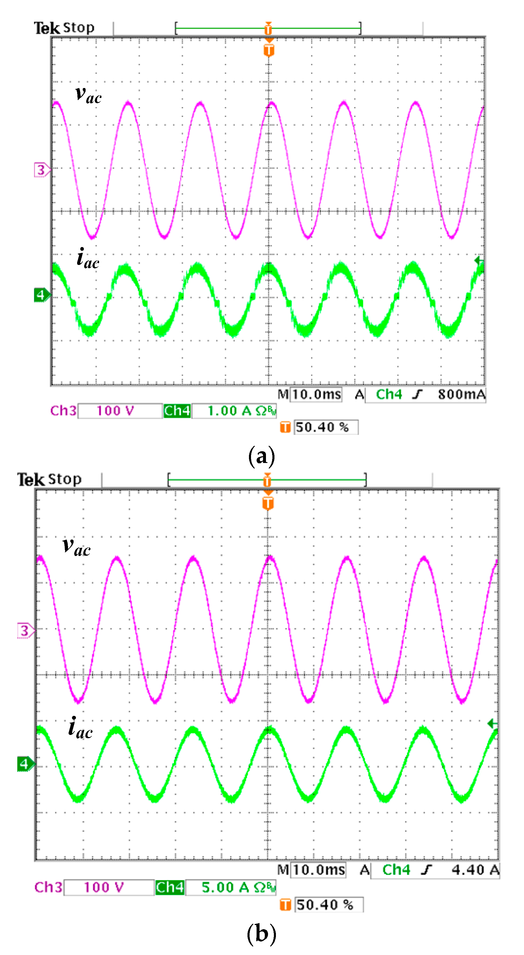
Figure 8a,b respectively represent the grid waveforms for output power PO = 40 W and PO = 300 W at an input voltage vac = 110 Vrms. The waveforms suggest that the proposed control strategy generates input line current waveforms that achieve phases almost perfectly consistent with that of the input line voltage waveforms. The results reveal that the boost PFC converter used according to the proposed method increases the system PF.
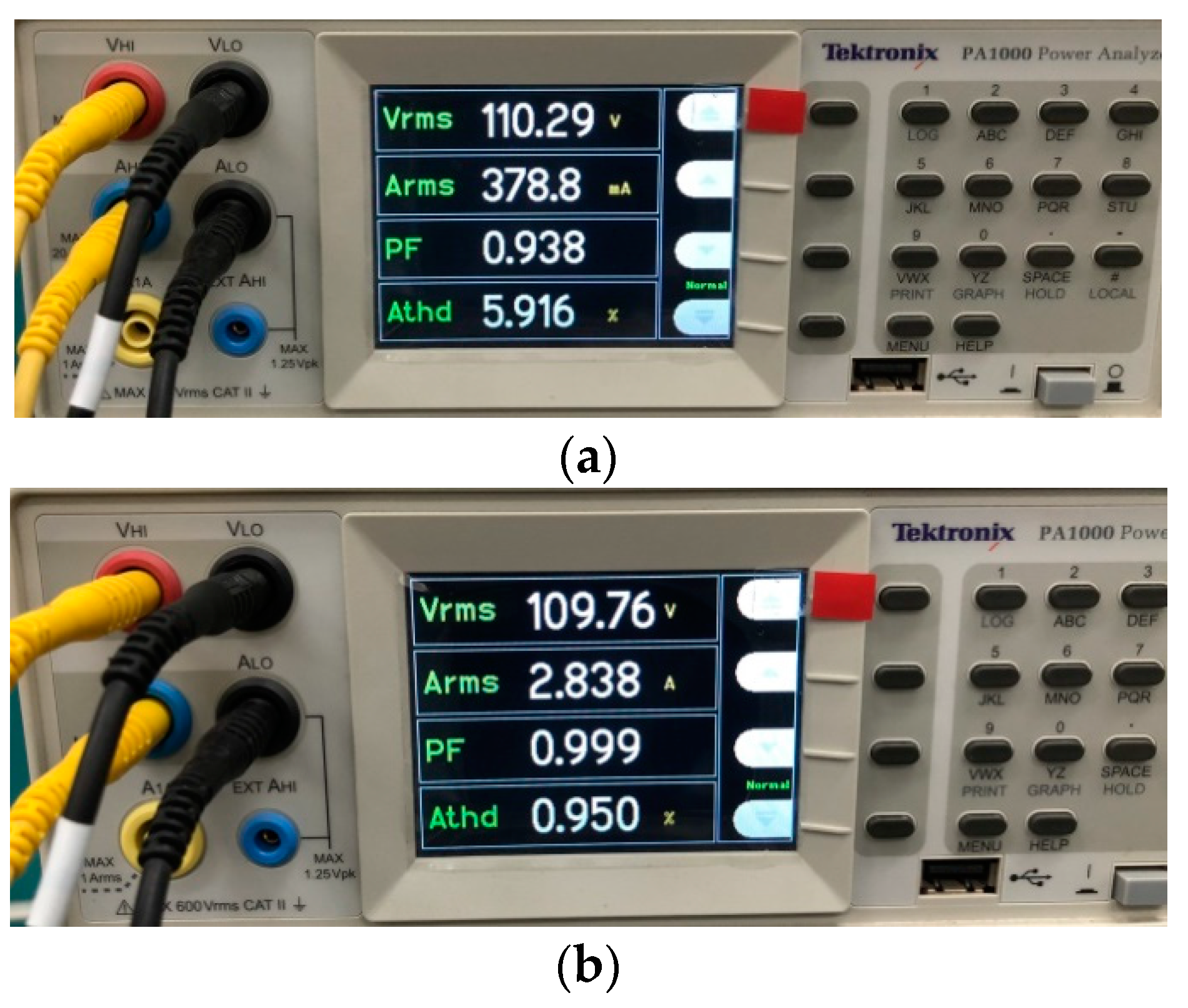
According to the experimental data, the proposed technique not only prevents effects on the PF but also resolves the ripple components of the twice-line frequency, improving the input line current THDi. These effects are obtained by measuring the input voltage in the following conditions: vac = 110 Vrms (PO = 40 W) and vac = 110 Vrms (PO = 300 W). The line current THDi values of both conditions were lower than 5.9%. In particular, the THDi at 300 W was 0.95%, as shown in Figure 9a,b.
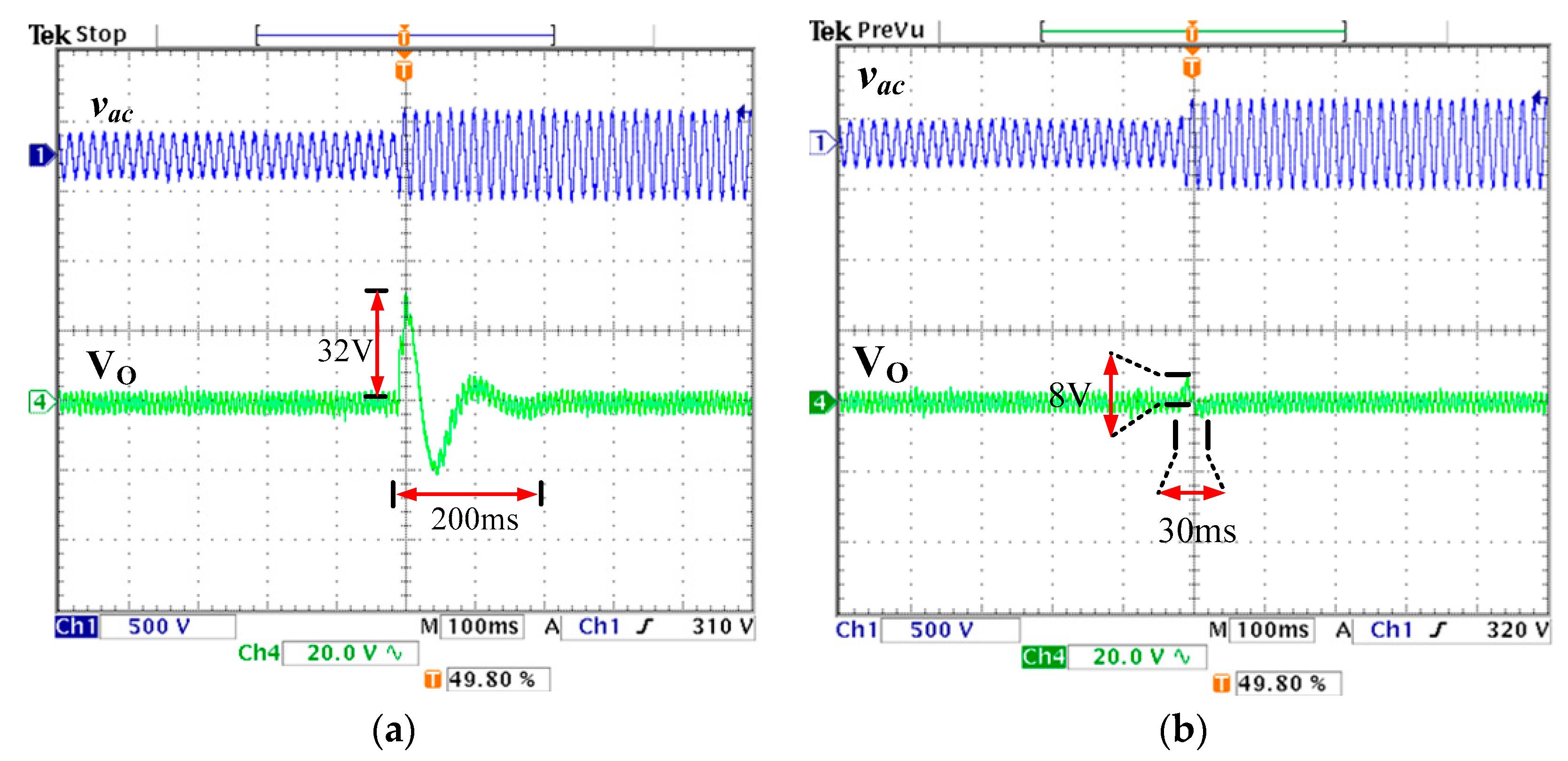
The proposed method requires no additional capacitor on the feedforward loop to attenuate second harmonic waves, and the bandwidth settings of the voltage loops are higher than in conventional methods. Therefore, the proposed control strategy realizes greater input transient response than conventional methods do, as shown in Figure 10 and Figure 11. Figure 10a depicts the input transient response measured in the conditions of input current THDi = 4% and output power PO = 300 W. According to Figure 10a, when the input voltage increased from 110 Vrms to 220 Vrm, the time for the output voltage to transfer from a transient state to a steady state was approximately 200 ms, and voltage maximum overshoot was approximately 32 V in the conventional method. The proposed method reduced the transient time by approximately 170 ms and voltage maximum overshoot by approximately 24 V, respectively, as depicted in Figure 10b. By contrast, in the same conditions, when the input voltage changed from 220 to 110 Vrms, the steady-state time and voltage maximum overshoot respectively exhibited 260-ms and 5-V differences, as shown in Figure 11a,b.
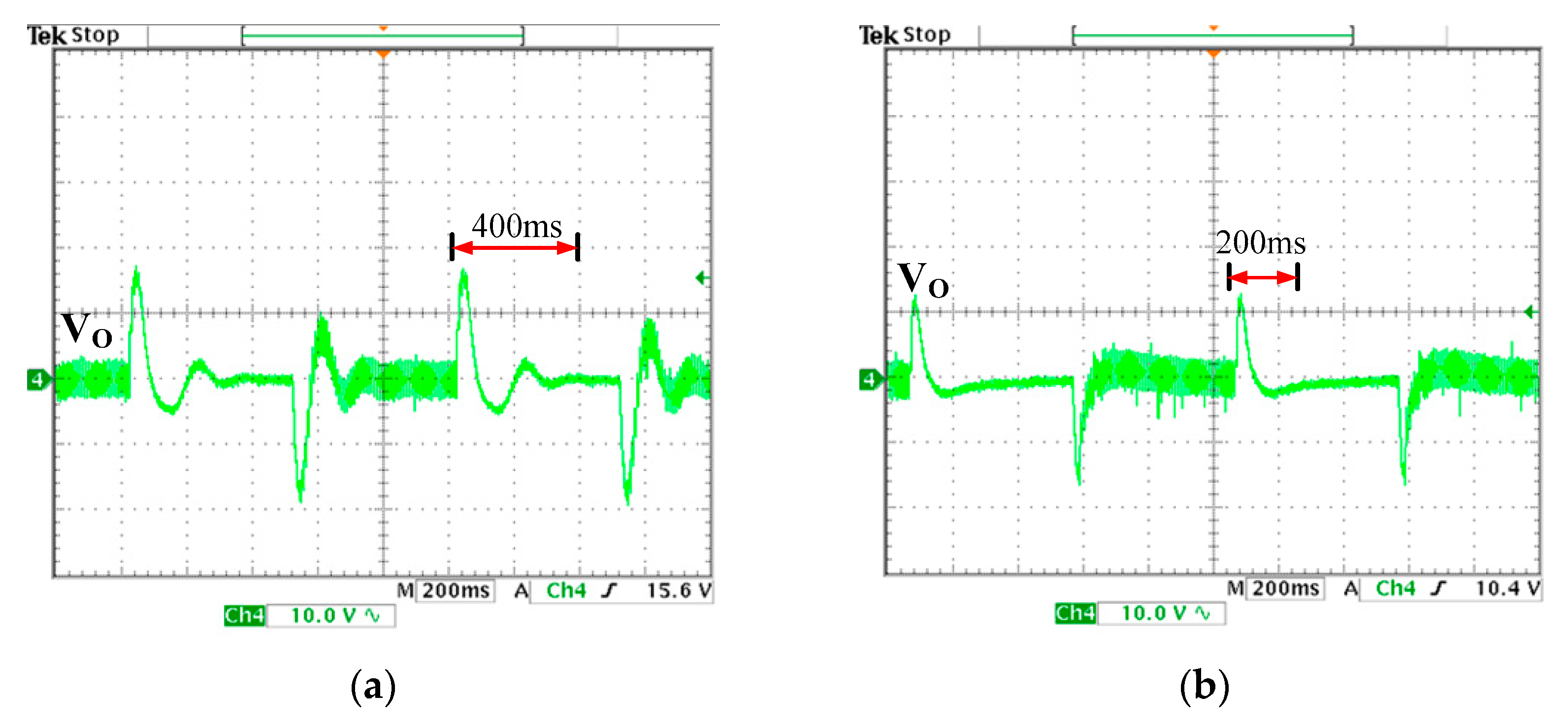
The output voltage transient responses for PFC with the use of conventional and proposed methods were compared. Figure 12a depicts the conventional PFC output voltage transient response (for output power conditions of light load 40 W and heavy load 300 W); Figure 12b depicts the new control strategy–based PFC output voltage transient response. The experimental data revealed that the conventional PFC output voltage transient response required approximately 400 ms to achieve a steady state, whereas the new PFC required approximately 200 ms. The proposed PFC was superior to the conventional one. The experimental data verified that the proposed method reduced input voltage and load transient response time.
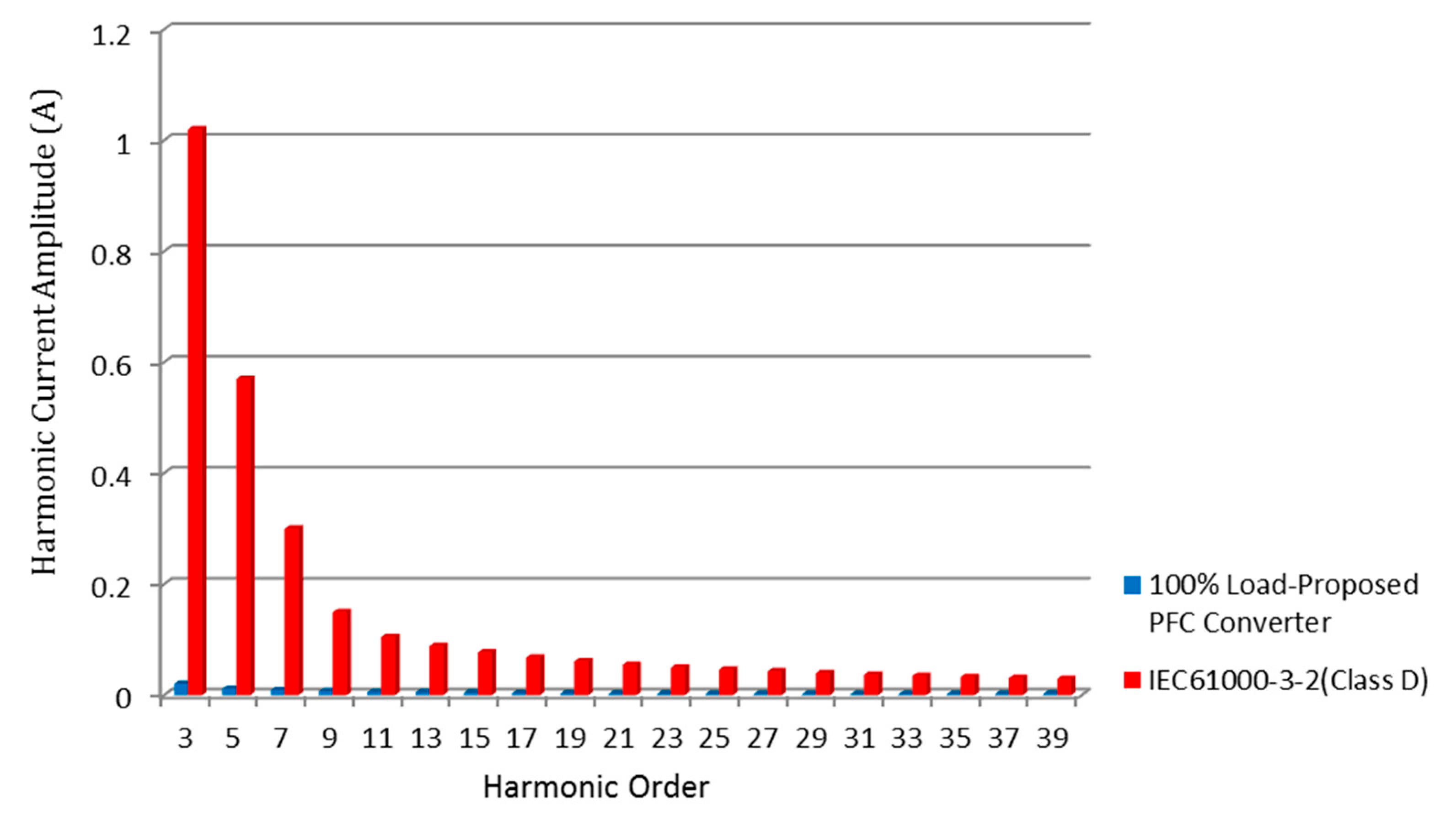
Table 3 demonstrates the relevant PFC measurement data yielded by the new control technique, including the PF value and input current THDi. The optimal input current THDi was approximately 0.9%. Finally, the testing condition was set for 110 V input voltage and 300 W output power. The standard of IEC 61000-3-2 (Class-D) was applied to compare with the proposed scheme, as shown in Figure 13. From this figure, the current harmonic for odd-harmonic of the proposed structure was much lower than the standard. Hence, the proposed scheme of this paper is feasible.
6. Conclusions
The paper proposed a control technique for PFC regulator operated in average current mode. The operation principle of the control technique has been discussed in detailed. A control technique for a 300 W Boost PFC regulator was developed, and it also performed very well. The paper has two advantages from the proposed control techniques. The first is that two sets of ADC and digital potential meter are placed at the feed forward voltage loop and the output voltage loop, respectively. There is no need to place extra multiplier and square circuit for lowering the complexity. The second is that the peak voltage detector and S/H circuit can sample the average value from the feed forward voltage loop and the output voltage loop; hence, there is no influence for 120 HZ ripple voltage. It helps to reduce the input current harmonic distortion. After that, a low frequency bandwidth filter is unnecessary. This will speed up the transient response from input voltage to the output load.
Author Contributions
Conceptualization, J.-M.W. and F.-Y.C.; methodology, S.-T.W. and M.-C.C.; validation, S.-T.W., F.-Y.C., M.-C.C., J.-M.W. and Y.-Y.S.; resources, J.-M.W. and S.-T.W.; writing—original draft preparation, J.-M.W.; writing—review and editing, J.-M.W. and S.-T.W. All authors have read and agreed to the published version of the manuscript.
Funding
This research was funded by Ministry of Science and Technology, R.O.C., grant number MOST 110-2622-E-150-002.
Conflicts of Interest
The authors declare no conflict of interest.
References
- Pressman, A.I. Switching Power Supply Design, 2nd ed.; McGraw-Hill: New York, NY, USA, 1998. [Google Scholar]
- Sakthivel, K.N.; Das, S.K.; Kini, K.R. Importance of quality AC power distribution and understanding of EMC standards IEC 61000-3-2, IEC 61000-3-3 and IEC 61000-3-11. In Proceedings of the 8th International Conference on Electromagnetic Interference and Compatibility, Chennai, India, 18–19 December 2003; pp. 423–430. [Google Scholar]
- Yang, C.; Liu, Y.; Tseng, P.; Pan, T.; Chiu, H.; Lo, Y. DSP-Based Interleaved Buck Power Factor Corrector with Adaptive Slope Compensation. IEEE Trans. Ind. Electron. 2015, 62, 4665–4677. [Google Scholar] [CrossRef]
- Holland, B. Modelling, analysis and compensation of the current-mode converter. Proc. Powercon. 1984, 11, I-2-1–I-2-6. [Google Scholar]
- Billings, K. Switchmode Power Supply Handbook, 2nd ed.; McGraw-Hill: New York, NY, USA, 1999. [Google Scholar]
- Todd, P.C. UC3854 Controlled Power Factor Correction Circuit Design; Appl. Note U-134; Unitrode: Watertown, MA, USA, 2003. [Google Scholar]
- Hwu, K.I.; Chen, H.W.; Yau, Y.T. Fully digitalized implementation of PFC rectifier in CCM without ADC. IEEE Trans. Power Electron. 2012, 27, 4021–4029. [Google Scholar] [CrossRef]
- Chiu, H.; Lo, Y.; Yang, C.; Cheng, S.; Huang, C.; Kou, M.; Huang, Y.; Jean, Y.; Huang, Y. A module-integrated isolated solar micro-inverter. IEEE Trans. Ind. Electron. 2013, 60, 781–788. [Google Scholar] [CrossRef]
- Wai, R.J.; Lin, C.Y. Active low-frequency ripple control for clean energy power-conditioning mechanism. IEEE Trans. Ind. Electron. 2010, 57, 3780–3792. [Google Scholar] [CrossRef]
- Tang, Y.; Zhu, D.; Jin, C.; Wang, P.; Blaabjerg, F. A three-level quasi two-stage single-phase PFC converter with flexible output voltage and improved conversion efficiency. IEEE Trans. Power Electron. 2015, 30, 717–726. [Google Scholar] [CrossRef]
- Chen, Y.; Chen, Y.; Chen, H. On-time compensation method for CRM/DCM Boost PFC converter. In Proceedings of the 2013 Twenty-Eighth Annual IEEE Applied Power Electronics Conference and Exposition, Long Beach, CA, USA, 17–21 March 2013; pp. 3096–3100. [Google Scholar]
- Rajagopalan, J.; Cho, J.G.; Cho, B.H.; Lee, F.C. High performance control of single-phase power factor correction circuits using a discrete time domain control method. In Proceedings of the 1995 IEEE Applied Power Electronics Conference and Exposition-APEC’9, Dallas, TX, USA, 5–9 March 1995; pp. 647–653. [Google Scholar]
- Chu, G.; Tse, C.K.; Wong, S.C.; Tan, S.C. A unified approach for the derivation of robust control for boost PFC converters. IEEE Trans. Power Electron. 2009, 24, 2531–2544. [Google Scholar] [CrossRef]
- Karaarslan, A.; Iskender, I. Average sliding control method applied on power factor correction converter for decreasing input current total harmonic distortion using digital signal processor. IET Power Electron. 2012, 5, 617–626. [Google Scholar] [CrossRef]
- Marcos-Pastor, A.; Vidal-Idiarte, E.; Cid-Pastor, A.; Salamero, L.M. Loss-free resistor-based power factor correction using a semibridgeless boost rectifier in sliding-mode control. IEEE Trans. Power Electron. 2015, 30, 5842–5853. [Google Scholar] [CrossRef] [Green Version]
- Marcos-Pastor, A.; Vidal-Idiarte, E.; Cid-Pastor, A.; Martinez-Salamero, L. Interleaved Digital Power Factor Correction Based on the Sliding-Mode Approach. IEEE Trans. Ind. Electron. 2016, 31, 4641–4653. [Google Scholar] [CrossRef]
- Zhang, F.; Xu, J. A Novel PCCM Boost PFC Converter with Fast Dynamic Response. IEEE Trans. Ind. Electron. 2011, 58, 4207–4216. [Google Scholar] [CrossRef]
- Hosseinzadeh, M.; Salmasi, F.R. Robust optimal power management system for a hybrid AC/DC micro-grid. IEEE Trans. Sustain. Energy 2015, 6, 675–687. [Google Scholar] [CrossRef]
- Rivera, J.; Ortega-Cisneros, S.; Chavira, F. Sliding Mode Output Regulation for a Boost Power Converter. Energies 2019, 12, 879. [Google Scholar] [CrossRef] [Green Version]
- Ahmed, M.; Kuisma, M.; Tolsa, K.; Silventoinen, P. Implementing sliding mode control for buck converter. In Proceedings of the IEEE 34th Annual Conference on Power Electronics Specialist, Acapulco, Mexico, 15–19 June 2003; Volume 2, pp. 634–637. [Google Scholar]
- Wall, S.; Jackson, R. Fast controller design for single-phase power-factor correction systems. IEEE Trans. Ind. Electron. 1997, 44, 654–660. [Google Scholar] [CrossRef]
- Franco, D.A.; Roberto, R.E.; Moreira, V.E.; Lessa, T.F. Experimental evaluation of active power factor correction techniques in a single-phase AC-DC boost converter. Int. J. Circuit Theory Appl. 2019, 47, 1529–1553. [Google Scholar] [CrossRef]
- Pandiev, I.M. Analysis and Behavioral Modeling of Monolithic Digital Potentiometers. IEEE Trans. Ind. Appl. 2017, 54, 416–425. [Google Scholar] [CrossRef]
- Huliehel, F.A.; Lee, F.C.; Cho, B.H. Small-signal modeling of the single-phase boost high power factor converter with constant frequency control. In Proceedings of the PESC’892 Record. 23rd Annual IEEE Power Electronics Specialists Conference, Toledo, Spain, 29 June–3 July 1992; Volume 1, pp. 475–482. [Google Scholar]
- Park, J.; Kim, D.J.; Lee, K. Predictive control algorithm including conduction-mode detection for PFC converter. IEEE Trans. Ind. Electron. 2016, 63, 5900–5911. [Google Scholar] [CrossRef]
- Zhang, W.; Feng, G.; Liu, Y.-F.; Wu, B. A digital power factor correction (PFC) control strategy optimized for DSP. IEEE Trans. Power Electron. 2004, 19, 1474–1485. [Google Scholar] [CrossRef]
- Erickson, R.W.; Maksimovic, D. Fundamentals of Power Electronics, 2nd ed.; Academic: Norwell, MA, USA, 2001. [Google Scholar]
- Mohan, Undeland and Robbins, Power Electronics, 2nd ed.; Wiley: New York, NY, USA, 1995.
Figure 1.
PFC regulators control scheme operating in the average current mode.

Figure 2.
Crucial command waveform.

Figure 3.
Proposed PFC control circuit block.

Figure 4.
(a) The proposed novel feedforward loop control circuit scheme; (b) relevant key waveforms.
Figure 4.
(a) The proposed novel feedforward loop control circuit scheme; (b) relevant key waveforms.

Figure 5.
The proposed feedforward loop circuit scheme.

Figure 6.
(a) The proposed new control strategy–based voltage feedback loop control circuit scheme; (b) relevant critical waveforms.
Figure 6.
(a) The proposed new control strategy–based voltage feedback loop control circuit scheme; (b) relevant critical waveforms.

Figure 7.
Resistance corresponding to various input voltage peaks.

Figure 8.
At an input voltage of 110 Vrms, the boost PFC input voltage and current waveforms with (a) output power of 40 W and (b) output power of 300 W (Vac: 100 V/div., iac: 1 A/div., Time: 10 ms/div.).
Figure 8.
At an input voltage of 110 Vrms, the boost PFC input voltage and current waveforms with (a) output power of 40 W and (b) output power of 300 W (Vac: 100 V/div., iac: 1 A/div., Time: 10 ms/div.).

Figure 9.
At an input voltage of 110 Vrms, the boost PFC input line current THDi with (a) output power of 40 W and (b) output power of 300 W.
Figure 9.
At an input voltage of 110 Vrms, the boost PFC input line current THDi with (a) output power of 40 W and (b) output power of 300 W.

Figure 10.
Transient response waveform of an input voltage change from 110 to 220 Vrms based on PFC with the use of (a) the conventional control strategy and (b) the new control strategy (Vac: 500 V/div., vO: 20 V/div., time: 100 ms/div.).
Figure 10.
Transient response waveform of an input voltage change from 110 to 220 Vrms based on PFC with the use of (a) the conventional control strategy and (b) the new control strategy (Vac: 500 V/div., vO: 20 V/div., time: 100 ms/div.).

Figure 11.
Transient response waveform of an input voltage change from 220 to 110 Vrms based on PFC with the use of (a) the conventional control strategy and (b) the new control strategy (Vac: 500 V/div., vO: 20 V/div., time: 100 ms/div.).
Figure 11.
Transient response waveform of an input voltage change from 220 to 110 Vrms based on PFC with the use of (a) the conventional control strategy and (b) the new control strategy (Vac: 500 V/div., vO: 20 V/div., time: 100 ms/div.).

Figure 12.
Output transient response waveform based on PFC with the use of (a) the conventional control strategy and (b) the new control strategy (Vac: 500 V/div., vO: 10 V/div., time: 200 ms/div).
Figure 12.
Output transient response waveform based on PFC with the use of (a) the conventional control strategy and (b) the new control strategy (Vac: 500 V/div., vO: 10 V/div., time: 200 ms/div).

Figure 13.
Comparison of current harmonic between the proposed structure and the standard of IEC61000-3-2 (Class-D) under the input voltage 110 V and output power 300 W.
Figure 13.
Comparison of current harmonic between the proposed structure and the standard of IEC61000-3-2 (Class-D) under the input voltage 110 V and output power 300 W.


Table 1.
TO-64 line decoder corresponding to input peak voltage.
| VFF(p) | Inputs | Outputs | ||||||||||
|---|---|---|---|---|---|---|---|---|---|---|---|---|
| A5 | A4 | A3 | A2 | A1 | A0 | D63 | D62 | D61 | … | D1 | D0 | |
| Vm64 | 0 | 0 | 0 | 0 | 0 | 0 | 0 | 0 | 0 | … | 0 | 1 |
| Vm63 | 0 | 0 | 0 | 0 | 0 | 1 | 0 | 0 | 0 | … | 1 | 0 |
| · · · | · · · | · · · | · · · | · · · | · · · | · · · | · · · | · · · | · · · | · · · | · · · | · · · |
| Vm3 | 1 | 1 | 1 | 1 | 0 | 1 | 0 | 0 | 1 | … | 0 | 0 |
| Vm2 | 1 | 1 | 1 | 1 | 1 | 0 | 0 | 1 | 0 | … | 0 | 0 |
| Vm1 | 1 | 1 | 1 | 1 | 1 | 1 | 1 | 0 | 0 | … | 0 | 0 |
Table 2.
Comparison of predictive ccm average current control technology and proposed ccm average current control technology for boost pfc converter.
Table 2.
Comparison of predictive ccm average current control technology and proposed ccm average current control technology for boost pfc converter.
| Computational Complexity | Difficulty of IC Integration | PI Controller Design Requirements | Cost | |
|---|---|---|---|---|
| Predictive CCM average current controller [25,26] | Medium | Large | No | High |
| Proposed CCM average current controller | Small | Small | Yes | Low |
Table 3.
Newly structured pf value and Thdi.
| Vin (Vrms) | VO (V) | IO (A) | PF (%) | THDi (%) |
|---|---|---|---|---|
| 110 | 385 | 0.100 | 0.939 | 5.91 |
| 110 | 385 | 0.175 | 0.977 | 3.24 |
| 110 | 385 | 0.260 | 0.989 | 1.92 |
| 110 | 385 | 0.340 | 0.993 | 1.37 |
| 110 | 385 | 0.420 | 0.996 | 1.14 |
| 110 | 385 | 0.500 | 0.997 | 1.06 |
| 110 | 385 | 0.573 | 0.998 | 1.01 |
| 110 | 385 | 0.650 | 0.999 | 0.97 |
| 110 | 385 | 0.723 | 0.999 | 0.98 |
Publisher’s Note: MDPI stays neutral with regard to jurisdictional claims in published maps and institutional affiliations. |
© 2021 by the authors. Licensee MDPI, Basel, Switzerland. This article is an open access article distributed under the terms and conditions of the Creative Commons Attribution (CC BY) license (https://creativecommons.org/licenses/by/4.0/).
Share and Cite
MDPI and ACS Style
Wu, S.-T.; Chen, F.-Y.; Chien, M.-C.; Wang, J.-M.; Su, Y.-Y. A Hybrid Control Scheme with Fast Transient and Low Harmonic for Boost PFC Converter. Electronics 2021, 10, 1848. https://0-doi-org.brum.beds.ac.uk/10.3390/electronics10151848
AMA Style
Wu S-T, Chen F-Y, Chien M-C, Wang J-M, Su Y-Y. A Hybrid Control Scheme with Fast Transient and Low Harmonic for Boost PFC Converter. Electronics. 2021; 10(15):1848. https://0-doi-org.brum.beds.ac.uk/10.3390/electronics10151848
Chicago/Turabian StyleWu, Sen-Tung, Fu-Yuan Chen, Min-Chu Chien, Jian-Min Wang, and Yan-Ying Su. 2021. "A Hybrid Control Scheme with Fast Transient and Low Harmonic for Boost PFC Converter" Electronics 10, no. 15: 1848. https://0-doi-org.brum.beds.ac.uk/10.3390/electronics10151848
Note that from the first issue of 2016, this journal uses article numbers instead of page numbers. See further details here.