
Analysis and Design for Output Voltage Regulation in Constant-on-Time-Controlled Fly-Buck Converter


Department of Energy and Electrical Engineering, Korea Polytechnic University, Siheung 15073, Korea
*
Author to whom correspondence should be addressed.
Electronics 2021, 10(16), 1886; https://0-doi-org.brum.beds.ac.uk/10.3390/electronics10161886
Submission received: 11 July 2021
/
Revised: 30 July 2021
/
Accepted: 2 August 2021
/
Published: 6 August 2021
(This article belongs to the Special Issue High Performance Power Converters: Design, Control, Devices and Applications)
Abstract
:Fly-buck converter is a multi-output converter with the structure of a synchronous buck converter structure on the primary side and a flyback converter structure on the secondary side, and can be utilized in various applications due to its many advantages. In terms of control, the primary side of the fly-buck converter has the same structure as a synchronous buck converter, allowing the constant-on-time (COT) control to be applied to the fly-buck converter. However, due to the inherent energy transfer principle, the primary-side output voltage regulation of COT controlled fly-buck converters may be poor, which can deteriorate the overall converter performance. Therefore, the primary output capacitor must be carefully designed to improve the voltage regulation characteristics. In this paper, a theoretical analysis of the output voltage regulation in COT controlled fly-buck converter is conducted, and based on this, a design guideline for the primary output capacitor considering the output voltage regulation is presented. The validity of the analysis and design guidelines was verified using a 5 W prototype of the COT controlled fly-buck converter for telecommunication auxiliary power supply.
1. Introduction
Multi-output converters can be utilized when different types of output voltages are required in power conversion applications. As the need for multi-output power supply in various industrial applications such as telecommunication equipment and medical devices increases, studies on multi-output converters with simple structure, high efficiency, and improved cross regulation characteristics are being actively conducted [1,2,3,4,5,6,7,8]. As part of these studies, a new multi-output converter called fly-buck converter has been proposed in [9]. The fly-buck converter has a combined structure of a synchronous buck converter structure on the primary side and a flyback converter structure on the secondary side. Hence, multiple outputs can be easily generated through the coupled inductor winding. In addition, it is known that the fly-buck converter has the following advantages:
- One power stage can supply tightly regulated non-isolated output and semi-regulated isolated outputs;
- Isolated outputs have high design freedom by using the duty cycle and turns ratio of the coupled inductor;
- Low price due to low number of components;
- High efficiency at light load due to zero voltage switching (ZVS) operation;
- Excellent control dynamics because it is controlled in a non-isolated form.
Based on these advantages, fly-buck converters can be used for several power supply applications, including gate drivers and dual supply amplifiers. A number of related studies have also been reported [10,11,12,13]. In [10], the design of the fly-buck converter used to provide IGBT gate driver bias was addressed. In [11], the cross-regulation characteristic between primary and secondary side outputs of the fly-buck converter is studied. In [12], a comparative study is presented on the time domain analysis of fly-buck converter with and without considering the effect of parasitic components.
In terms of fly-buck converter control, the primary side of the fly-buck converter has the same structure as the synchronous buck converter, so the control techniques applicable to the synchronous buck converter such as voltage mode control, hysteresis control, constant-on-time (COT) control can be used as it is. Among them, COT control is one of the most commonly used control techniques. Since COT control does not require a loop compensation network, it can achieve a fast transient response and make design easier. Accordingly, in [13], COT control has been applied to the fly-buck converter. In particular, the literature compared the control dynamic and voltage regulation when voltage mode control and COT control were, respectively, applied to a fly-buck converter. As a result, in COT control, the control dynamic was excellent, but the voltage regulation characteristic was inferior.
The poor voltage regulation characteristic when applying COT control is due to the inherent operating principle of the fly-buck converter. Unlike other conventional topologies, the non-isolated primary side output capacitor acts as an intermediate in energy transferring to the isolated outputs in the fly-buck converter. Therefore, the heavier the load on the isolated secondary side or the smaller the primary output capacitor, the larger the ripple voltage on the primary side, which adversely affects the primary side voltage regulation of the COT controlled fly-buck converter. Moreover, since the secondary output voltage is indirectly controlled by the primary output voltage and the turns ratio of the coupled inductor, the regulation of the primary output voltage must be treated as important for the overall converter performance. Due to these properties, the primary side output capacitor must be chosen very carefully when designing a fly-buck converter. However, there is no literature dealing with this design issue as far as the authors are concerned. Therefore, this paper aims to identify the cause of the phenomenon through the steady-state analysis of the fly-buck converter and propose a design guideline for the primary-side output capacitor based on the analysis.
This paper is organized as follows. Section 2 describes the steady-state analysis of the fly-buck converter. Section 3 analyzes the relationship between the primary output capacitor and the primary output voltage ripple regarding output voltage regulation, and establishes design guidelines for the primary output capacitor design. In Section 4, the experimental results verify the overall content of the analysis made. Finally, the conclusion of the paper is discussed in Section 5.
2. Operating Principle of the Fly-Buck Converter
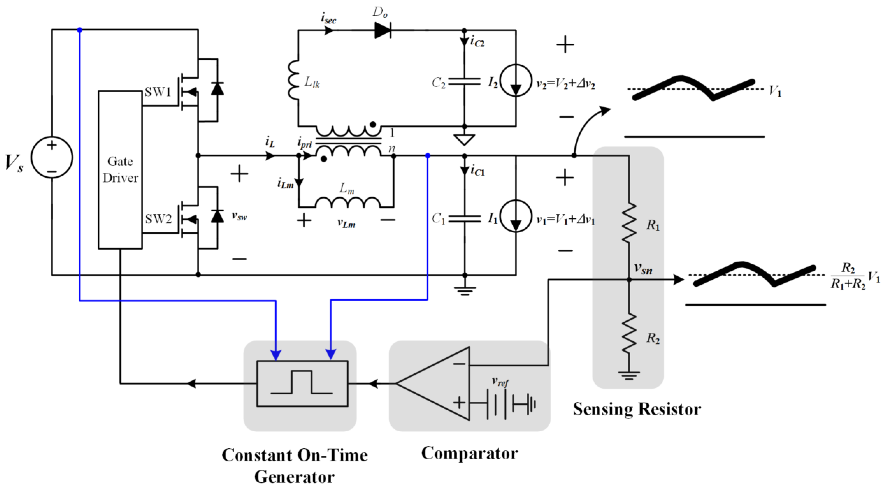
The circuit configuration of the fly-buck converter is shown in Figure 1. The non-isolated primary side has the same structure as the synchronous buck converter except that a coupled inductor is used in place of the output inductor. The coupled inductor has a turns ratio of n:1 and is modeled using the magnetizing inductance, Lm, and leakage inductance reflected on the secondary side, Llk. SW1 and SW2 act as high side switch and low side switch of the synchronous buck converter. C1 and I1 represent the primary output capacitor and the primary load current. On the secondary, Do, C2, and I2 refer to the output diode, secondary output capacitor, and secondary load current, respectively.
The following describes the voltage symbols indicated in Figure 1. Vs is the input voltage, v1(t) and v2(t) are the primary and secondary output voltages, V1 and V2 are the DC value of the primary and secondary output voltages, and Δv1(t) and Δv2(t) are the ripple components of v1(t) and v2(t), respectively. vsw(t) is the voltage across the low side switch, and vLm(t) is the voltage across the magnetizing inductance.
The following describes the current symbols indicated in Figure 1. I1, I2, ic1(t), and ic2(t) are the primary side load current, the secondary side load current, and the current flowing into C1 and C2, respectively. Additionally, iLm(t) is the current flowing through a magnetizing inductance, and ipri(t) and isec(t) are the currents flowing through the primary and secondary sides of the coupled inductor. Finally, iL(t) represents the sum of ipri(t) and iLm(t).
The operation modes of the fly-buck converter are shown in Figure 2. The overall operation is divided into a buck mode in which SW1 is turned on (SW2 is turned off) and a flyback mode in which SW2 is turned on (SW1 is turned off). In actual operation, the modes can be further subdivided due to the effects of dead time and parasitic components, but in this paper, the analysis proceeds based on these two modes for the convenience of analysis. Figure 3 shows the steady-state waveforms based on the two modes.
2.1. Buck Mode
The circuit operation in buck mode is shown in Figure 2a. During the interval [t0, t1], because a negative voltage is applied to Do, Do does not conduct, and energy is not transferred to the secondary side. Therefore, it operates the same as when the high side switch of the synchronous buck is turned on. In this mode, the basic equations of a circuit are expressed as
2.2. Flyback Mode
The circuit operation in flyback mode is shown in Figure 2b. During the interval [t1, t3], the primary side operates as the freewheeling mode of the synchronous buck converter. On the secondary side, Do starts to conduct and acts similar to a flyback converter. In this mode, the basic equations of a circuit are expressed as
In more detail, the configuration of the primary and secondary sides in the flyback mode can be expressed as Figure 4a. By reflecting the primary side into the secondary side, the equivalent circuit in Figure 4b can be obtained. Here, for the convenience of analysis, assuming that the impedance of the Lm is large enough, the equivalent circuit can be simplified as shown in Figure 4c. From Figure 4c, it can be seen that the fly-buck converter operates by the resonance of Llk, C1, and C2, unlike the conventional flyback converter during flyback mode operation.
From Equations (5)–(8) and the differential equation of the resonance mode, isec(t) and v2(t) can be expressed as
where Ceq is the equivalent capacitor which can be obtained as
2.3. Voltage Gain
For the non-isolated primary output, since the operation is exactly the same as that of the synchronous buck converter, the relationship between the input voltage and the output voltage is expressed as
where D is the duty cycle of the fly-buck converter.
The exact output voltage equation can be expressed as Equation (10) for the isolated secondary output. However, it is difficult to use it as a design formula for its complexity. In general, Llk is a reasonably small value, so if ignored, Equation (10) can approximately be represented as:
However, it should be noted that if Llk is not negligibly small, the V2 will drop as the I2 increases. Consequently, with respect to the indirectly controlled V2, how small the Llk is has a significant impact on cross regulation performance.
3. Analysis on the Output Voltage Regulation of COT Controlled Fly-Buck Converter
As stated in Section 1, the non-isolated primary side output capacitor in the fly-buck converter acts as an intermediate in energy transferring to the isolated outputs, unlike other conventional topologies. Therefore, the heavier the load on the isolated secondary side or the smaller the primary output capacitor, the larger the ripple voltage, Δv1(t), on the primary side.
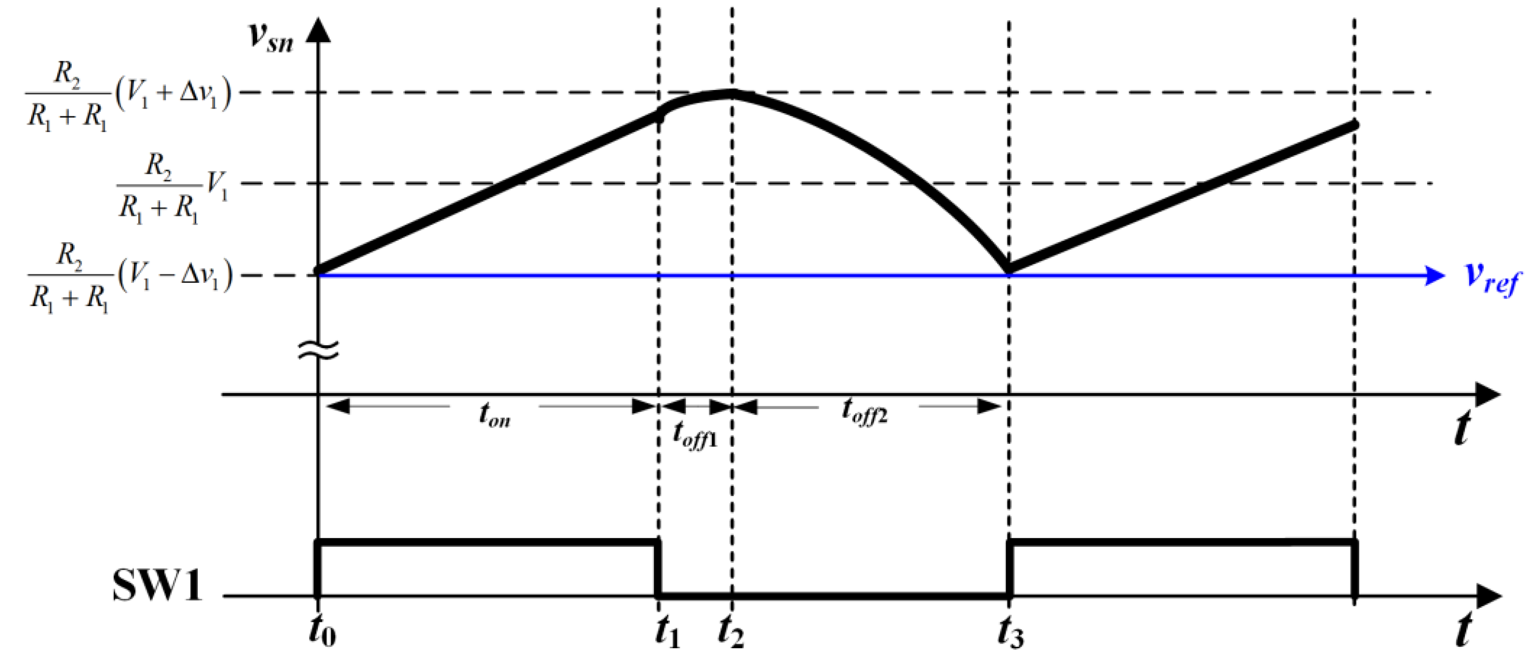
Figure 5 shows the block diagram of the COT controlled fly-buck converter. In COT control, the turn-on signal of SW1 is generated when the minimum value of the sensed output voltage, vsn(t), becomes smaller than the reference voltage, vref. Therefore, when the magnitude of Δv1(t) increases, V1 value moves away from the reference value, and the voltage regulation deteriorates. It can be understood more intuitively in Figure 6 that shows the enlarged waveform of the sensed output voltage.
The magnitude of Δv1(t) is affected by C1 and the amount of energy transferred to the secondary side. Meanwhile, the secondary side load current corresponds to the input in the two-port network that supplies the voltage source output and thus cannot be chosen by the designer. Thus, the only design factor related to the magnitude of Δv1(t) is C1, and by designing it correctly, the voltage regulation can be maintained within the desired range.
In this section, C1 and output voltage regulation characteristics are analyzed more quantitatively, and design guidelines are established from the results of the analysis.
3.1. The Relation between Primary Output Capacitor and Voltage Regulation
In the steady-state operation of the converter, in one cycle, the charge amount and the discharge amount in the capacitor must be equal by the charge balance. Furthermore, the following physical equation must be satisfied from the basic properties of the capacitor
where ΔQ is the amount of change in charge, C is the capacitance, and ΔV is the amount of change in voltage. Let us apply these principles to the fly-buck converter.
ΔQ = CΔV,
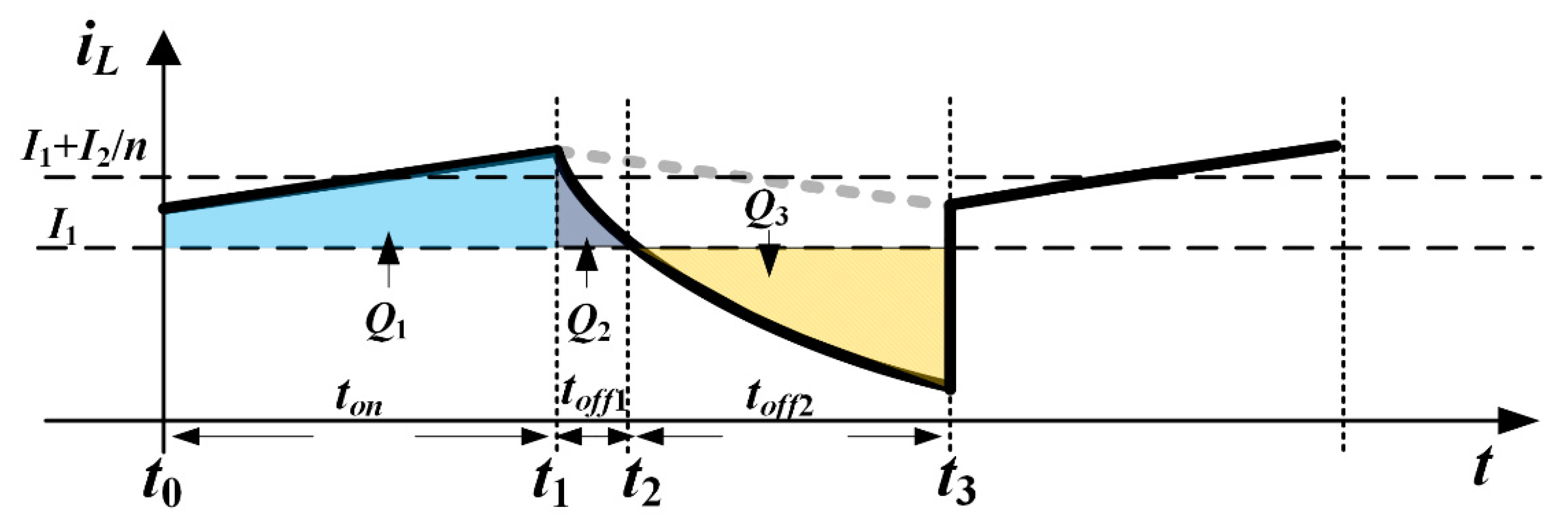
Figure 7 shows the steady-state waveform of iL in the primary side of the fly-buck converter. From Figure 7, it can be seen that the charge amount of C1 is the sum of Q1 and Q2, and the discharge amount is Q3. Therefore, in the fly-buck converter, Equation (14) can be rearranged as:
Q1 + Q2 = Q3 = 2C1Δv1.
If Q1 and Q2 are quantitatively represented using circuit parameters, we can get an intuition for circuit design with improved output voltage regulation.
As for Q1, using Equations (2) and (4) in buck mode, it can be expressed as:
where ton is the on-time determined by the COT generator.
As for Q2, using Equations (6), (8), and (9) and assuming that Lm is large enough in flyback mode, ic1(t) in the time interval [t1, t2] is obtained as:
Assuming the following condition, which is generally not difficult to meet,
the cosine term and the sine term in Equation (17) can be approximated as follows:
From the result of the assumption, Equation (17) can be rewritten as:
Using the above results, Q2 can be expressed as:
where t2 is the time when iL is equal to I1 and can be obtained as:
As a result, using Equations (15), (16), and (22), Δv1 can be calculated as:
and a voltage offset of Δv1 is generated in V1, which can deteriorate voltage regulation.
3.2. Design Guideline for the Primary Output Capacitor
If V1/n = V2 is assumed for the convenience of analysis, Equation (23) can be approximated as
and, consequently, Q2 can also be approximated as
Then, the charge amount of C1 is
Therefore, if the desired Δv1 is determined, C1 should be designed as
Equation (28) confirms that C1 should be designed to consider the energy transferred to the secondary side from a voltage regulation perspective. However, since Ceq is a value dependent on C1 as in Equation (11), Equation (28) cannot be directly used as a design criterion. Therefore, Equation (28) can be rearranged assuming the following two cases.
The first case is C2 << n2C1, where Ceq can be approximated to C2, hence, Equation (28) can be rearranged as:
The second case is C2 >> n2C1, where Ceq can be approximated to n2C1, hence, Equation (28) can be summarized as:
The analysis results were applied to a specific target application of the 5 W telecommunication auxiliary power supply. The system specifications are summarized in Table 1, and the design parameters of the COT controlled fly-buck converter excluding C1 are summarized in Table 2.
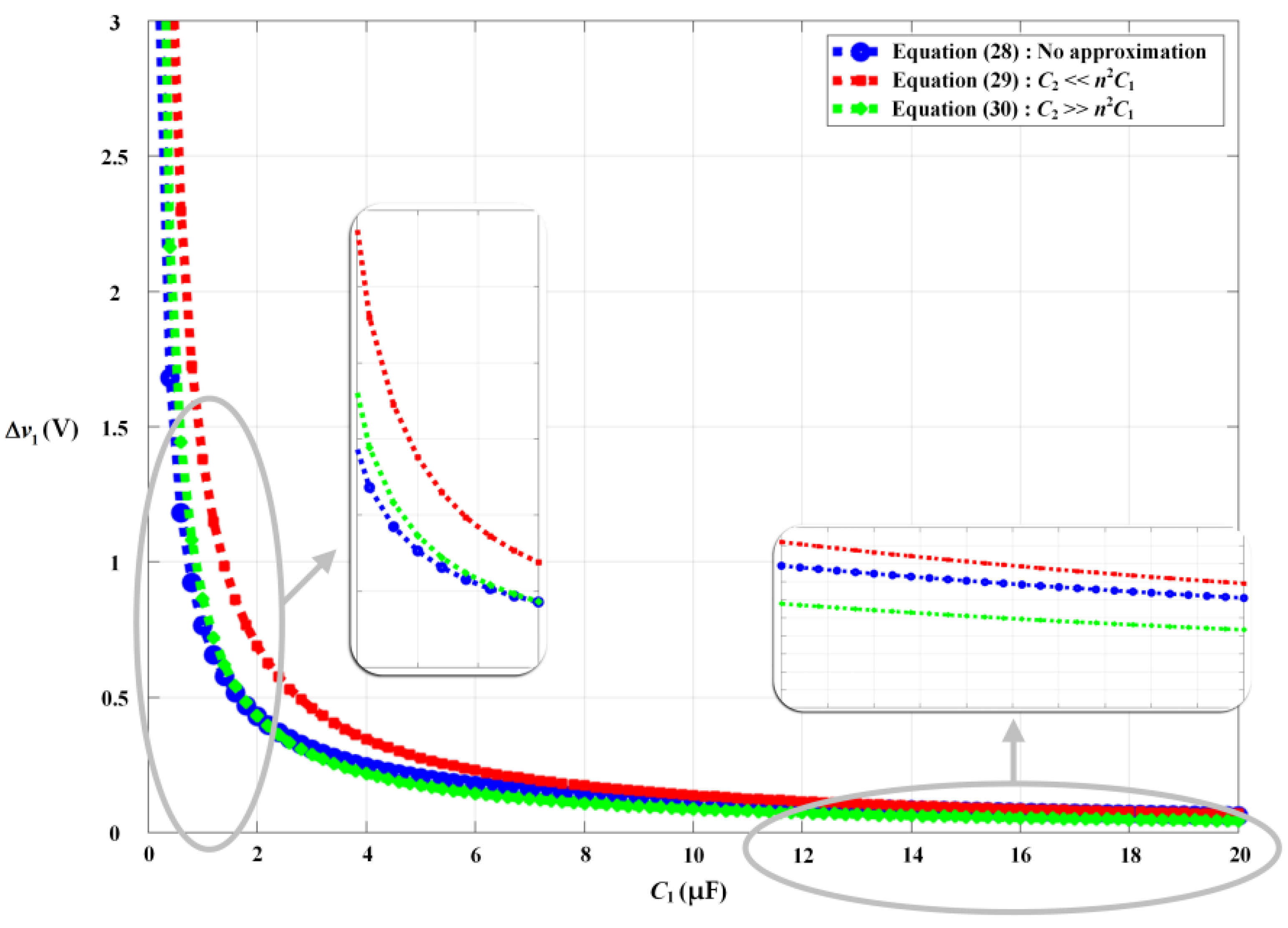
Figure 8 shows the change in Δv1 according to the design of C1 at rated power in the fly-buck converter designed with the parameters in Table 1 and Table 2. In Figure 8, it can be seen that the approximation of C2 >> n2C1 is more accurate in the region where C1 is small and vice versa in the region where C1 is large. From the above, it was confirmed that by using Equations (29) and (30), C1 can be designed in consideration of the secondary load from the viewpoint of output voltage regulation. Therefore, the COT controlled fly-buck converter can be designed using a suitable approximation for target applications. Additionally, based on Equations (29) and (30) and Figure 8, it can be seen that the larger C1 is, the more desirable in terms of voltage regulation. However, COT control is performed based on the ripple of the output voltage. Therefore, if C1 is too large, the ripple magnitude will be too small to control, which must additionally reflect the ripple generation technique that can complicate the overall system. Consequently, in a COT-controlled fly-buck converter, C1 must be designed large enough to satisfy the desired voltage regulation, but at the same time be small enough to generate a ripple voltage for COT control.
4. Experimental Result
A prototype of a COT controlled fly-buck converter was built and tested for a 5 W telecommunication auxiliary power supply to verify the validity of the analysis. The values in Table 1 and Table 2 were used for the system specifications for the experimental and design parameters, respectively. The LM5017 IC was used to implement COT control. Meanwhile, a multilayer ceramic capacitor (MLCC) was used as an output capacitor, which has the characteristic that the capacitance changes according to the DC bias voltage [14]. Therefore, for accurate experimental data, the voltage ripple value according to the current input/output was measured at the DC bias value to be tested, and the obtained equivalent capacitance from these data was used for the experiment.
First, to verify the effect of the energy transferred to the secondary on the voltage regulation, C1 was designed as 10 μF and then the experiment was conducted by gradually increasing the secondary load current. The experimental waveforms of the voltage across the low side switch (vsw(t)), the sum of the currents flowing through the magnetizing inductor and the primary side coupled inductor (iL(t)), the primary side output voltage (v1(t)) and the secondary output voltage(v2(t)) of the fly-buck converter are shown in Figure 9a,b. The experimental conditions are when the secondary load power P2 is 1 W and 5 W, respectively. When P2 is 1 W, V1 is 12.145 V, and when P2 is 5 W, V1 is 12.464 V, which is consistent with the analysis that voltage regulation characteristics worsen as the secondary load increases. Additionally, as can be seen from Equation (10), it was also confirmed that V2 decreased as the secondary load current increased.
Next, to check the changes in the ripple voltage according to the design of C1, Δv1 and Δv2 were observed while changing C1 in a situation where the primary output power, P1, and the secondary output power, P2, were set to 1 W. Δv1 and Δv2 were observed by magnifying the output voltage in AC coupling mode. Figure 10a,b show the experimental waveforms when C1 is 390 nF and 10 μF, respectively. When the noise component is excluded in Figure 10a where C1 is 390 nF, Δv1 is observed to be about 260 mV, while in case of Figure 10b where C1 is 10 μF, Δv1 is observed to be about 10 mV. These experimental results show that the smaller C1, the greater the Δv1, and the higher the operating frequency as v1 discharges faster. On the other hand, in the case of Δv2, since C2 and P2 do not change, it shows a value that hardly changes.
Figure 11 is a graph drawn by comparing calculated Δv1 by Equation (28) with the observed Δv1 and Δv2 excluding switching noise while increasing C1 from 390 nF to 10 μF. As can be seen, for Δv1, there is a small error, but the overall trend is consistent with the analysis. In contrast, for Δv2, since the values of C2 and P2 are constant, almost the same value is maintained regardless of C1. Thus, the validity of the analysis was verified through experiments, and it was confirmed that C1 should be designed in the consideration of the load power transferred to the secondary side in order to improve the voltage regulation characteristics.
5. Conclusions
In the fly-buck converter, the non-isolated primary side output capacitor, C1, acts as an intermediate in energy transferring to the isolated outputs. Therefore, the heavier the load on the isolated secondary side or the smaller the primary output capacitor, the larger the ripple voltage on the primary side, which adversely affects the primary side output voltage regulation and may lead to deterioration of the overall converter performance in the COT controlled fly-buck converter. Due to these properties, the primary side output capacitor must be chosen very carefully.
In this paper, first, steady-state analysis, which is the basis for output voltage regulation analysis in a COT controlled fly-buck converter, was performed. Next, a theoretical analysis of the output voltage regulation in COT controlled fly-buck converter is conducted, and based on this, a design guideline for C1 considering the output voltage regulation is proposed. According to the obtained design guidelines, the primary output capacitor should be designed large enough to have a ripple voltage smaller than a certain Δv1, taking into account the secondary load from the standpoint of output voltage regulation. However, since COT control is performed based on the ripple of the output voltage, if the C1 is too large, the ripple magnitude will be too small to control, which must additionally reflect the ripple generation technique that can complicate the overall system. Consequently, in a COT controlled fly-buck converter, the C1 must be designed large enough to satisfy the desired voltage regulation, but at the same time be small enough to generate a ripple voltage for COT control.
To verify the validity of the analysis, a prototype of COT controlled fly-buck converter was built and tested for a 5 W telecommunication auxiliary power supply. First, to verify the effect of the energy transferred to the secondary on the voltage regulation, the C1 was designed as 10 μF and then the experiment was conducted by gradually increasing the secondary load power, P2. From the experimental result, when P2 was 1 W and 5 W, V1 was observed to be 12.145 V and 12.464 V, respectively, which is consistent with the analysis that voltage regulation characteristics worsen as the secondary load increases. Next, to check the changes in the ripple voltage according to the design of the C1, Δv1 and Δv2 were observed while changing the C1 in a situation where the primary output power and the secondary output power were set to 1 W. When the noise component was excluded from the measurement, Δv1 was observed to be about 260 mV and 10 mV when C1 was 390 nF and 10 μF, respectively. On the other hand, for Δv2, almost the same value is maintained regardless of C1. From the results above, the validity of the analysis was verified through experiments, and it was confirmed that C1 should be designed in the consideration of the load power transferred to the secondary side in order to improve the voltage regulation characteristics.
Author Contributions
Conceptualization, Y.C. and P.J.; methodology, Y.C. and P.J.; software, Y.C. and P.J.; validation, Y.C. and P.J.; formal analysis, Y.C.; investigation, Y.C.; resources, Y.C.; data curation, Y.C.; writing—original draft preparation, Y.C.; writing—review and editing, P.J.; visualization, Y.C. and P.J.; supervision, P.J.; project administration, P.J.; funding acquisition, P.J. All authors have read and agreed to the published version of the manuscript.
Funding
This work was supported by the National Research Foundation of Korea (NRF) grant funded by the Korea government (MSIT) (No. 2018R1C1B5086194).
Institutional Review Board Statement
Not applicable.
Informed Consent Statement
Not applicable.
Data Availability Statement
All data used in this research is available upon requirement.
Conflicts of Interest
The authors declare no conflict of interest.
References
- Wai, R.-J.; Jheng, K.-H. High-efficiency single-input multiple-output DC–DC converter. IEEE Trans. Power Electron. 2013, 28, 886–898. [Google Scholar] [CrossRef]
- Wai, R.-J.; Liaw, J.-J. High-efficiency isolated single-input multiple output bidirectional converter. IEEE Trans. Power Electron. 2015, 30, 4914–4930. [Google Scholar] [CrossRef]
- Tosun, G.; Kivanc, O.-C.; Oguz, E.; Ustun, O.; Tuncay, R.N. Development of High Efficiency Multi-Output Flyback Converter for Industrial Applications. In Proceedings of the ELECO’15, Bursa, Turkey, 26–28 November 2015; pp. 1102–1108. [Google Scholar]
- Tahan, M.; Bamgboje, D.; Hu, T. Flyback-based Multiple Output Dc-Dc Converter with Independent Voltage Regulation. In Proceedings of the 9th IEEE International Symposium on Power Electronics for Distributed Generation Systems, Charlotte, NC, USA, 25–28 June 2018. [Google Scholar]
- Marzuki, A.; Wibisono, G.; Hudaya, C. Design of Single Input Multiple Output Full Bridges DC-DC Converters for Personal Computer Power Supply. In Proceeding of the IEEE International Conference on Innovative Research and Development (ICIRD), Jakarta, Indonesia, 28–30 June 2019. [Google Scholar]
- Nayak, G.; Nath, S. Decoupled Voltage-Mode Control of Coupled Inductor Single-Input Dual-Output Buck Converter. IEEE Trans. Ind. App. 2020, 56, 4040–4050. [Google Scholar] [CrossRef]
- Park, H.; Kim, S. Single Inductor Multiple Output Auto-Buck-Boost DC–DC Converter with Error-Driven Randomized Control. Electronics 2020, 9, 1335. [Google Scholar] [CrossRef]
- Leng, C.-M.; Chiu, H.-J. Three-Output Flyback Converter with Synchronous Rectification for Improving Cross-Regulation and Efficiency. Electronics 2021, 10, 430. [Google Scholar] [CrossRef]
- Karlsson, M.; Persson, O. Isolated Fly-Buck Converter, Switched Mode Power Supply, and Method of Measuring a Voltage on a Secondary Side of an Isolated Fly-Buck Converter. U.S. Patent 137852, 17 September 2015. [Google Scholar]
- Fang, X.; Meng, Y. Isolated bias power supply for IGBT gate drives using the fly-buck converter. In Proceeding of the IEEE APEC, Charlotte, NC, USA, 15–19 March 2015; pp. 2373–2379. [Google Scholar]
- Wang, W.; Lu, D.; Chai, Q.; Lin, Q.; Cai, F. Analysis of fly-buck converter with emphasis on its cross-regulation. IET Power Electron. 2017, 10, 292–301. [Google Scholar] [CrossRef]
- Myneni, S.-B.; Samanta, S. Time Domain Analysis of Isolated Buck (F1y-Buck) Converter. In Proceedings of the 2018 IEEE International Conference on Power Electronics, Drives and Energy Systems (PEDES), Chennai, India, 18–21 December 2018. [Google Scholar]
- Myneni, S.-B.; Samanta, S. A Comparative Study of Different Control strategies for Isolated Buck (Fly-Buck) Converter. In Proceedings of the 2018 IEEE International Conference on Power Electronics, Drives and Energy Systems (PEDES), Chennai, India, 18–21 December 2018. [Google Scholar]
- Menzi, D.; Bortis, D.; Zulauf, G.; Heller, M.; Kolar, J.W. Novel iGSE-C Loss Modeling of X7R Ceramic Capacitors. IEEE Trans. Power Electron. 2020, 35, 13367–13383. [Google Scholar] [CrossRef]

Figure 2.
Operation modes of the fly-buck converter: (a) Buck mode; (b) Flyback mode.

Figure 3.
Steady-state waveform of the fly-buck converter.

Figure 4.
Equivalent circuit of the fly-buck converter in flyback mode: (a) Basic equivalent circuit; (b) Equivalent circuit when the primary side is reflected to the secondary side; (c) Equivalent circuit when Lm is large enough.
Figure 4.
Equivalent circuit of the fly-buck converter in flyback mode: (a) Basic equivalent circuit; (b) Equivalent circuit when the primary side is reflected to the secondary side; (c) Equivalent circuit when Lm is large enough.

Figure 5.
Block diagram of the COT controlled fly-buck converter.

Figure 6.
The enlarged waveform of the sensed output voltage.

Figure 7.
Steady-state waveform of iL in the primary side of the fly-buck converter.

Figure 8.
Δv1 according to C1 design.

Figure 9.
Experimental waveform of fly-buck converter: (a) C1 = 10 μF and P2 = 1 W; (b) C1 = 10 μF and P2 = 5 W.
Figure 9.
Experimental waveform of fly-buck converter: (a) C1 = 10 μF and P2 = 1 W; (b) C1 = 10 μF and P2 = 5 W.

Figure 10.
Experimental waveform of fly-buck converter: (a) C1 = 390 nF and P1 = P2 = 1 W; (b) C1 = 10 μF and P1 = P2 = 1 W.
Figure 10.
Experimental waveform of fly-buck converter: (a) C1 = 390 nF and P1 = P2 = 1 W; (b) C1 = 10 μF and P1 = P2 = 1 W.

Figure 11.
Experimental result of Δv1 and Δv2 according to C1 design.


Table 1.
System specification.
| Input voltage (Vs) | 24 V |
| Primary output voltage (V1) | 12 V |
| Secondary output voltage (V2) | 12 V |
| Rated power (Prate) | 5 W |
Table 2.
Design parameters of the COT controlled fly-buck converter.
| Constant-on time (ton) | 2.4 μs |
| Secondary output capacitor (C2) | 10 μF |
| Magnetizing inductance (Lm) | 250 μH |
| Leakage inductance (Llk) | 2 μH |
| Transformer turns ratio (n) | 1:1 |
Publisher’s Note: MDPI stays neutral with regard to jurisdictional claims in published maps and institutional affiliations. |
© 2021 by the authors. Licensee MDPI, Basel, Switzerland. This article is an open access article distributed under the terms and conditions of the Creative Commons Attribution (CC BY) license (https://creativecommons.org/licenses/by/4.0/).
Share and Cite
MDPI and ACS Style
Cho, Y.; Jang, P. Analysis and Design for Output Voltage Regulation in Constant-on-Time-Controlled Fly-Buck Converter. Electronics 2021, 10, 1886. https://0-doi-org.brum.beds.ac.uk/10.3390/electronics10161886
AMA Style
Cho Y, Jang P. Analysis and Design for Output Voltage Regulation in Constant-on-Time-Controlled Fly-Buck Converter. Electronics. 2021; 10(16):1886. https://0-doi-org.brum.beds.ac.uk/10.3390/electronics10161886
Chicago/Turabian StyleCho, Younghoon, and Paul Jang. 2021. "Analysis and Design for Output Voltage Regulation in Constant-on-Time-Controlled Fly-Buck Converter" Electronics 10, no. 16: 1886. https://0-doi-org.brum.beds.ac.uk/10.3390/electronics10161886
Note that from the first issue of 2016, this journal uses article numbers instead of page numbers. See further details here.