1. Introduction
The exponential data growth rates needed for the development of applications such as 5G, IoT, space, etc., led to the research of a new architecture for digital communications called the High-Speed Serial Link (HSSL). Power consumption, operational frequency, surface area, jitter, etc. represent various constraints that transceiver systems need to consider and remedy. As observation satellites require higher resolution image quality, the operating data traffic also needs to be increased. Adding to this, efficient power consumption systems need to be optimized since they directly affect the circuit lifetime. The last parameter of focus is the optimization of integration density, i.e., the chip area.
In our case, the targeted operating frequency, while aiming to reduce the area, consumption, and the locking time, is 3.2 GHz. A 300 MHz bandwidth is at least needed to ensure proper functioning while considering the potential variations implied by the Process Voltage Temperature (PVT) effects. To prevent those effects, [
1] demonstrates temperature and process compensation techniques which consist of reducing the influence of the variations on the circuit. For instance, the resistance of the loop filter (
R) needs to be large enough to compensate for the temperature variations.
Many solutions also imply the use of a Phase Locked Loop (PLL) circuit which shows interesting benefits such as low jitter, which is required for data link applications [
2,
3]. Due to the necessity to obtain the lowest jitter, most PLL circuits are based on LC-type oscillators. Indeed, these kinds of oscillators offer better phase noise and jitter performances than their counterparts, ring oscillators.
Nevertheless, knowing that the architecture of ring oscillators is inductor-less, a superior shrink capability than LC-type oscillators is apparent. Although the phase noise and jitter performances seem poorer than the LC-type, this inconvenience is avoided thanks to the injection locking mechanism.
Moreover, the PLL-based clock recovery circuit deals with the final issue, the locking time. To address this bottleneck, injection locking enables the possibility of drastically reducing this duration [
4]. Many studies have also shown that the injection-locking process naturally hardens the oscillator in its environment [
4,
5,
6,
7]. Since our work is dedicated to space application, this last issue is of great interest. Due to the extremely harsh environment, evidence of degradations induced by emitted particles from the Sun, the terrestrial magnetosphere, or cosmic radiations appears. As [
8,
9] demonstrated, the injection locking mechanism shows a great robustness improvement when the circuit is exposed to radiations.
The final parameter of our focus is the area. Since our work is destined to be implemented on satellites, the density integration is a major parameter for optimization.
Section 2 begins with a theoretical approach to the injection locking process. Then, a circuit description of each sub element constituting the circuit architecture is detailed in
Section 3. A technology overview as well as the circuit fabrication is given in
Section 4.
Section 5 entails the obtained measurement results and compares this work with similar state-of-the-art studies. A discussion of those results and some explanations are tackled in
Section 6. Lastly, a conclusion summarizes the work achieved in
Section 7.
2. Injection-Locking Theory
Before diving into the different elements constituting the circuit, a theoretical approach to the injection locking process is spelled out hereafter. Multiple approaches to injection locking on oscillators already exist. The most classic and widely known comes from Adler’s equations [
6]. Based on these, Razavi [
7] performed further development and gave additional clarifications. Both of those studies are dedicated to LC oscillators. Unfortunately, two major constraints emerge when the injection locking on ring oscillators is studied. Firstly, it is based on the idea that only one dominant pole exists. Secondly, it is necessary to know the quality factor (
Q), which is usually too complex to accurately quantify in the case of ring oscillators [
10,
11]. An analytical method to describe the injection-locking mechanism on ring oscillators is introduced by [
12] through phase noise and jitter calculations.
Ref. [
13] also describes in its theory the injection locking process operating on ring oscillators and gives a method to estimate the locking range. To satisfy the Barkhausen criteria to obtain oscillations, the total phase shift into the loop needs to be a multiple of 2π, implying a phase shift of π/N of each stage inverter.
When an injected signal (
Iinj) is applied to the ring oscillator, the oscillation frequency deviates from its free-running value
f0, and the injection-locking phenomenon appears [
6,
7]. With an input injection equal to
finj =
f0 + Δ
f, an additional phase shift of
ϕ is introduced into the loop by the injected stage.
In its theory, the general Adler’s phase equation is expressed as:
where Δ
(
t) is the phase difference between the oscillator and the injected signal,
f1 is the perturbation signal frequency,
f0 is the oscillator natural frequency, and
is the sinusoidal function of Δ
(
t). This equation is valid for any oscillator.
In the work [
13], Adler develops this theory, yielding it suitable for ring oscillators. To adapt Equation (1) to ring oscillators, the new expression of
with a sinusoidal injection signal is given as:
The phase lock occurs when is 0.
From this, the locking range is calculated as the maximum value of
g(Δ
φ(
t)).
where
R is the line resistance between each amplification stage,
Iinj is the injected current, and
A is the gain.
Finally, the locking range is given as .
The expression leads to this observation: for a given injection strength ( where Iosc is the current of the free-running oscillator), the locking range (Δf/f0) decreases as the number of stages (N) increases.
The injection locking process now defined, we will now delve into the details of the designed circuit.
3. Circuit Description
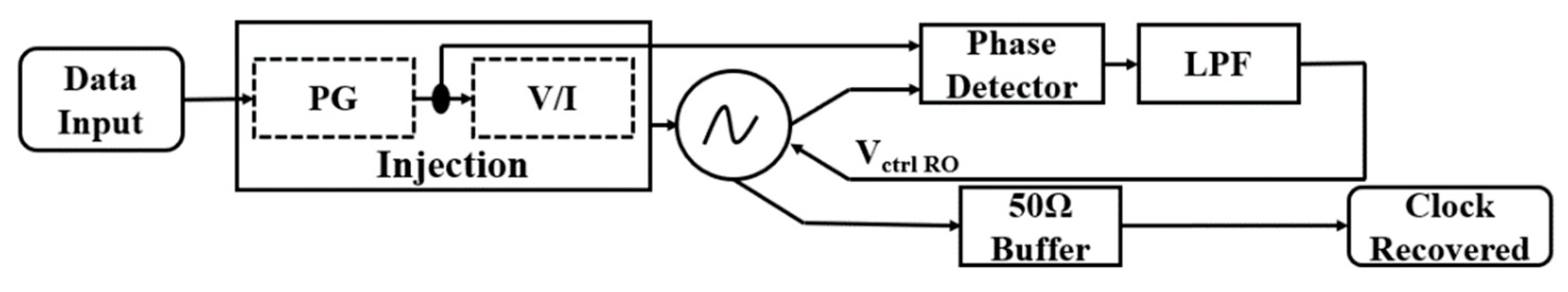
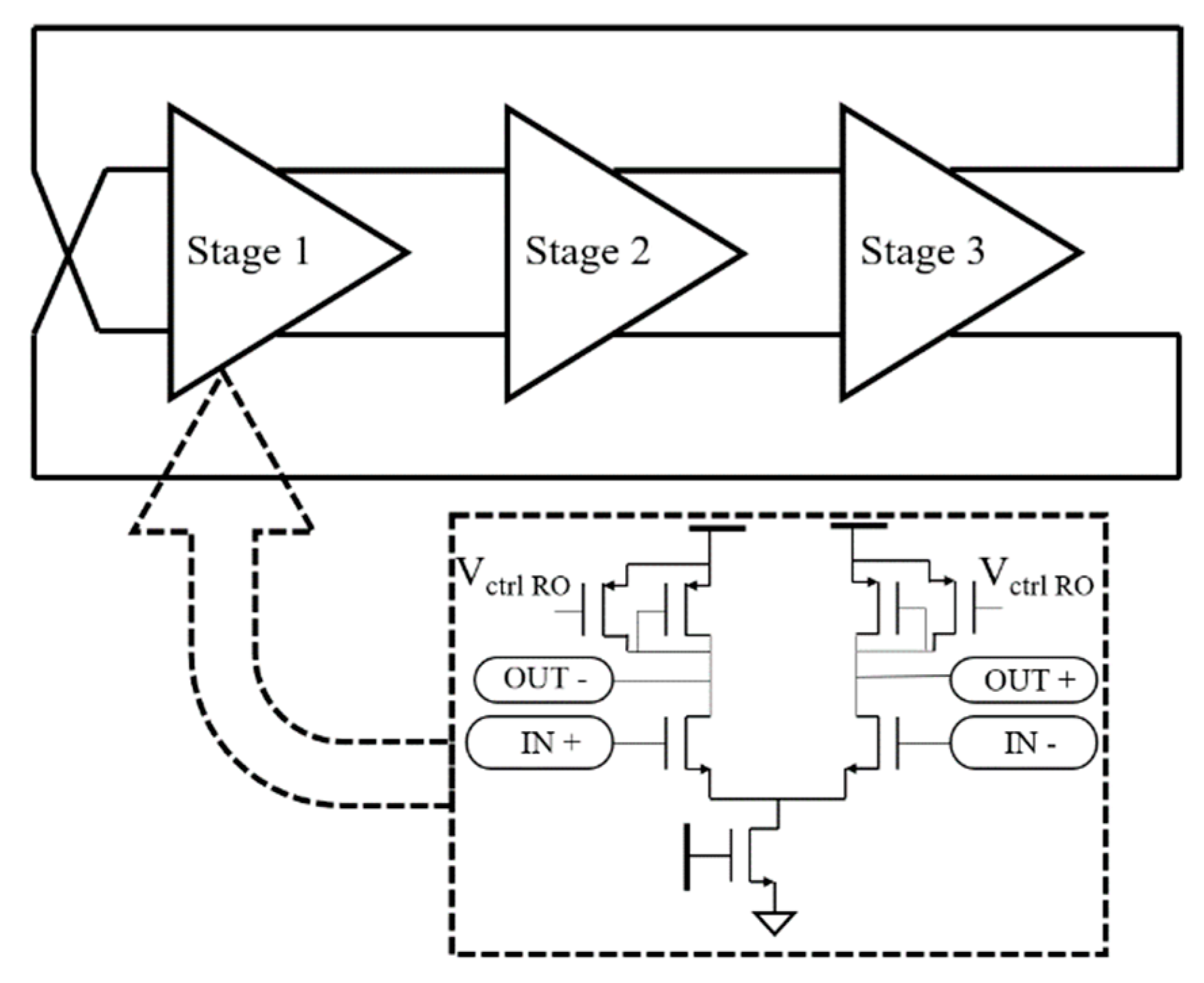
The designed architecture is composed of five elemental blocks, respectively named, a pulse generator (PG) creating the voltage pulses needed to enable the injection locking process, a Voltage-to-Current converter (V/I) converting the voltage pulses into current ones, an injection-locked ring oscillator generating the operational frequency, a phase detector (Phase Detector) comparing the input data sequences with the oscillator output signal, and finally a low-pass filter (LPF) constituting the loop filter of the PLL.
Knowing that the input data stream is represented as a Random Binary Sequence, there is a possibility in which a long sequence of identical bits (also called runlength) happens. Concerning the injection-locked ring oscillator, this can possibly lead to loss of the injection locking and so unsynchronize it from the target frequency. The goal of the PLL is to maintain this synchronization even in a presence of a long runlength thanks to the capture range provided by its loop filter.
Figure 1 gives an overview of the whole designed architecture.
To give more insights into the designed architecture, we describe the five elementary components in the next sub-sections.
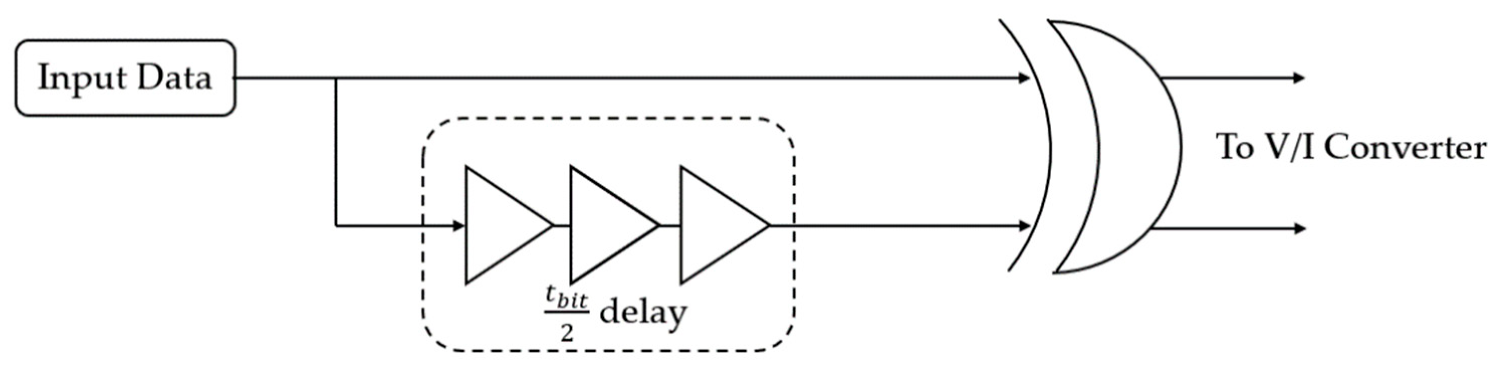
3.1. Pulse Generator
The Pulse Generator (PG, from
Figure 1) injects and ensures the synchronization of the ring oscillator at the target frequency of 3.2 GHz. The input data stream is sent through two paths with one delay.
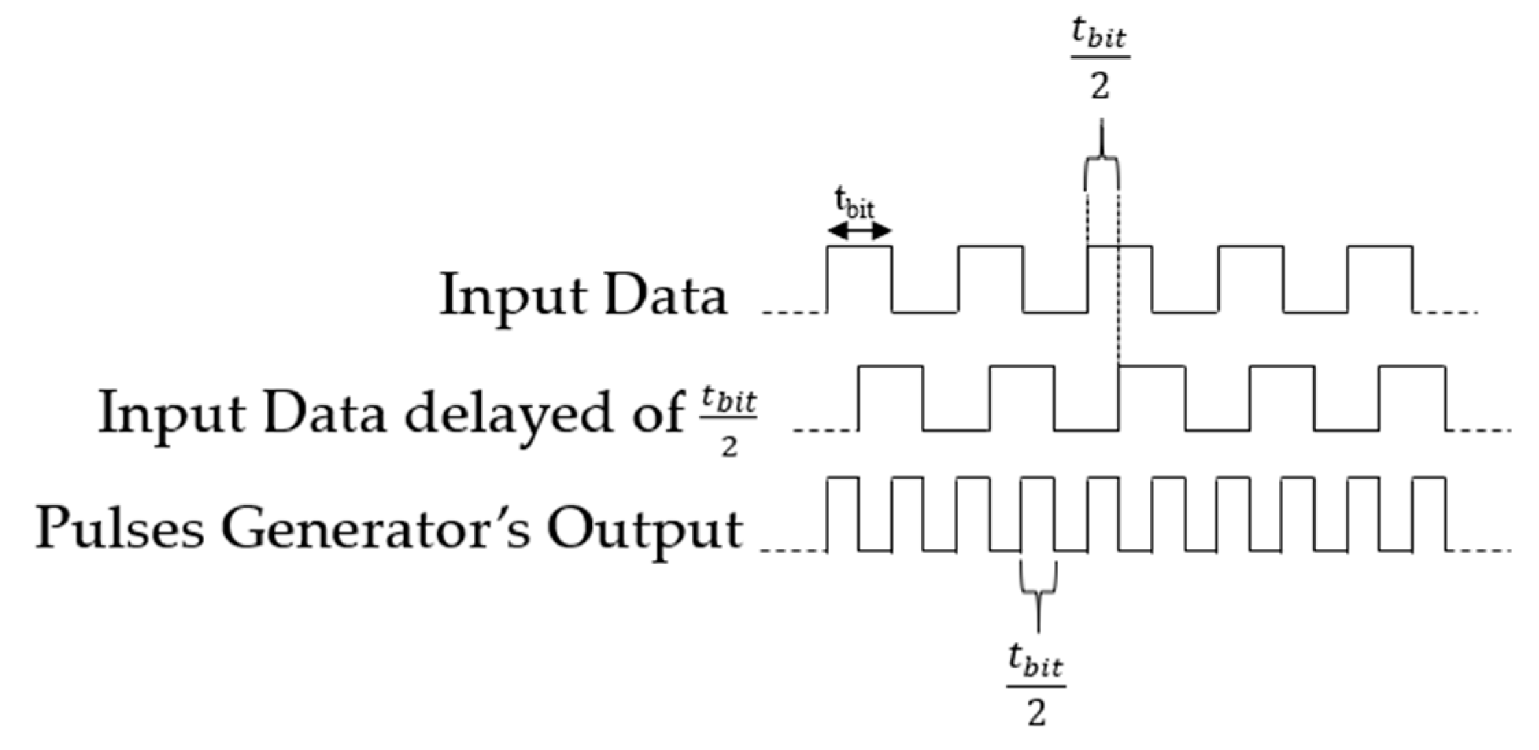
Figure 2 and
Figure 3 give the schematic and the chronogram of the PG, respectively.
To create sufficient pulses to operate the synchronization by injection, a delay of
is added in one of the two paths. Then, both of these paths constitute the two inputs of an XOR gate. The output of this generates the resultant voltage pulses and, as shown in
Figure 1, is connected to the next sub-element: the V/I converter.
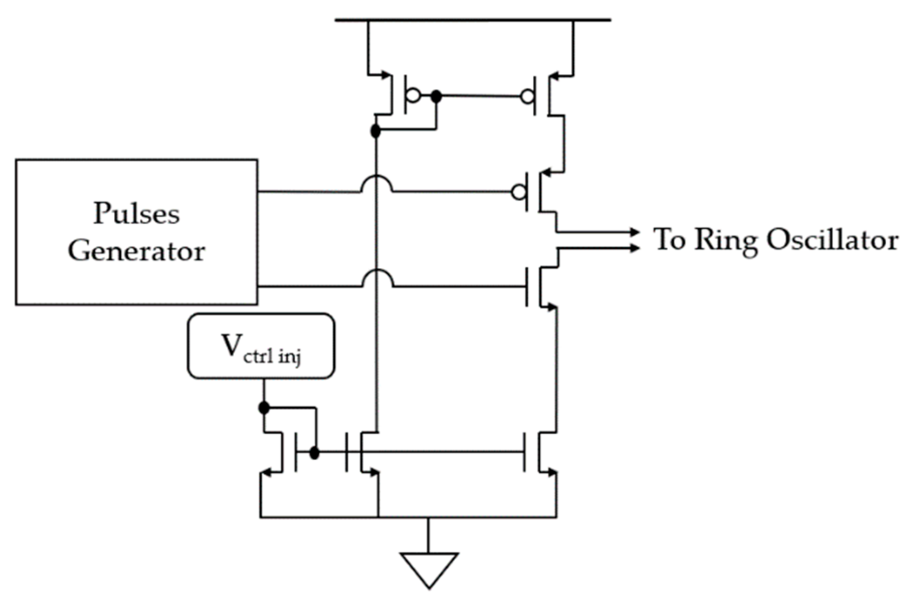
3.2. Voltage-to-Current Converter
In order to operate a correct injection-locking process, these voltage pulses need to be converted into current ones. This is the goal of the V/I converter described here and shown in
Figure 4.
The output of this element is then directly connected to the ring oscillator to effectively achieve synchronization by injection. The conversion is handled by the Nmos and Pmos output transistors and is connected to the first stage of the ring oscillator. An additional input (Vctrl inj) is added to tune the applied injection strength.
3.3. Ring Oscillator
The ring oscillator is composed of three stages of differential inverters. The main asset of the differential mode compared to the single mode comes from its better rejection noise stemming from the substrate and power supply.
The oscillator delivers a differential voltage whose peak-to-peak amplitude is constant with a tunable frequency. The Pmos active loads are used to tune the output oscillation frequency linearly via a control voltage,
Vctrl RO. As [
14] shows, the free-running frequency is given by:
where
N is the number of inverter stages and
td is the stage delay time.
Figure 5 gives the illustration of the designed ring oscillator schematic.
Two main explanations motivate the choice of the design of a three stages ring oscillator.
The first one, as Equation (4) indicates, the operating frequency is directly inversely proportional to the number of amplification stages, meaning, the lower the number of amplification stages, the higher the operating frequency achievable.
The second explanation comes from the objective to minimize the number of amplification stages to improve the tracking range, as the theory suggests.
3.4. Phase Detector and Loop Filter
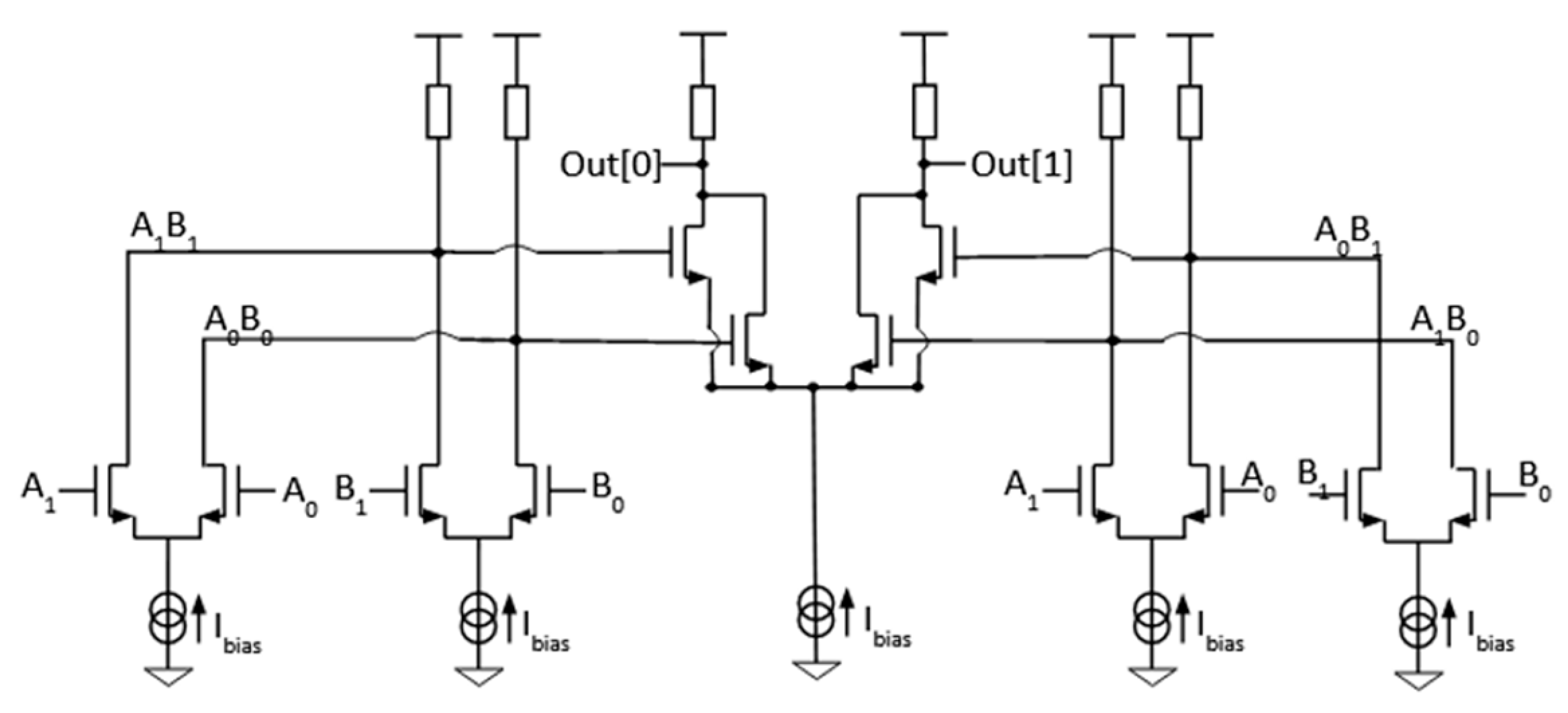
The main role of the phase detector is to compare the phase difference between the injected signal and the output of the ring oscillator. The produced error signal is proportional to the phase difference between its two inputs.
Figure 6 shows the schematic of the XOR-based fully symmetrical phase detector.
In this architecture, a fully symmetrical exclusive OR (XOR) gate plays this role. Thanks to two combined Gilbert cells, this architecture generates a signal with the same delay for each path [
15]. The loop filter sizing contributes as a key factor since its value gives the synchronization range of the PLL circuit.
In our case, since the target frequency () is 3.2 GHz, the ideal designed is 400 MHz.
4. Circuit Overview
As detailed in the introduction, the circuit has been manufactured in the XFAB 180 nm CMOS technology with a power supply of 1.8 V. Thanks to simulation, the transition frequency of about 45 GHz has been estimated. The choice of this technology has been motivated due to its inherent hardening to space radiations [
16,
17].
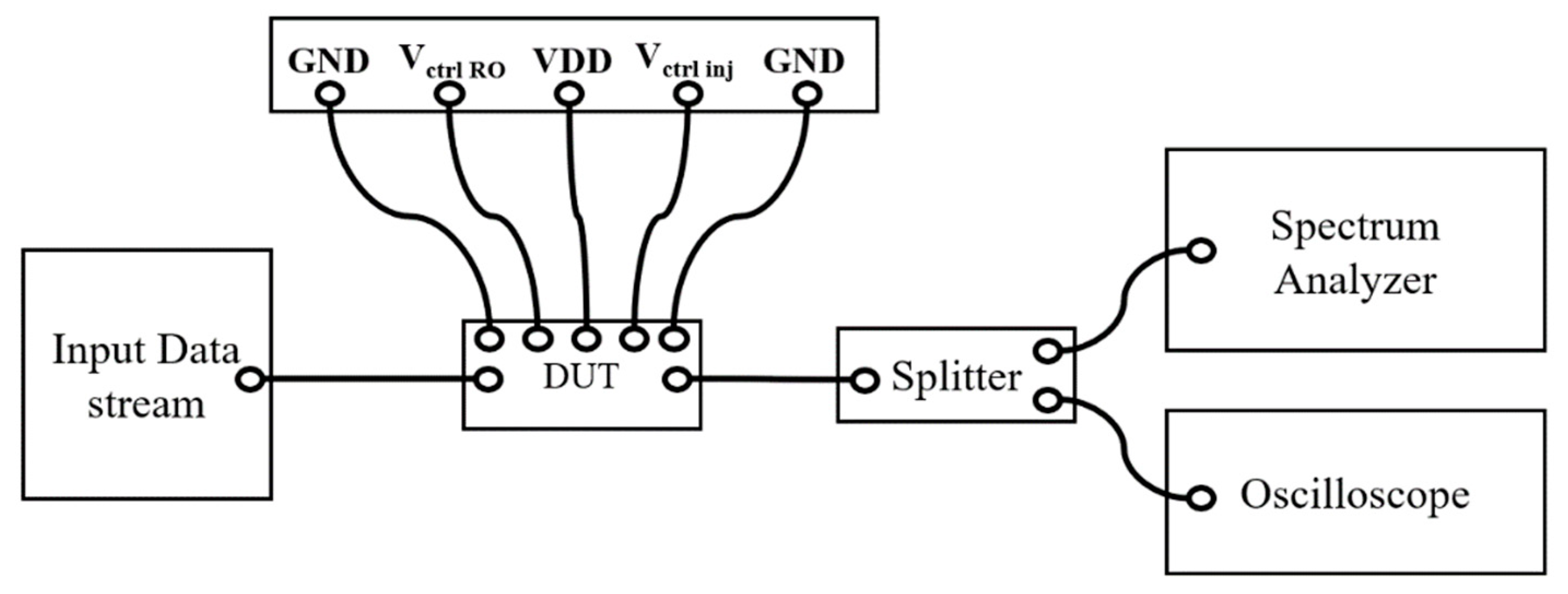
This circuit has been designed in order to be tested with spectral and transient measurements under probes up to 4 GHz.
The six DC pads placed at the north position of the chip are, from left to right, for grounding, Vctrl RO (to manually tune the frequency of the ring oscillator), Vctrl inj (to tune the injection strength of the signal), VDD, Vctrl Buffer 50Ω (to optimize the measured signal through the oscilloscope and the spectrum analyzer), and another ground.
The three RF pads placed at the west and east sides of the chip correspond to the input and output of the circuit, respectively. Both the input and output are Ground/Signal/Ground RF pad types.
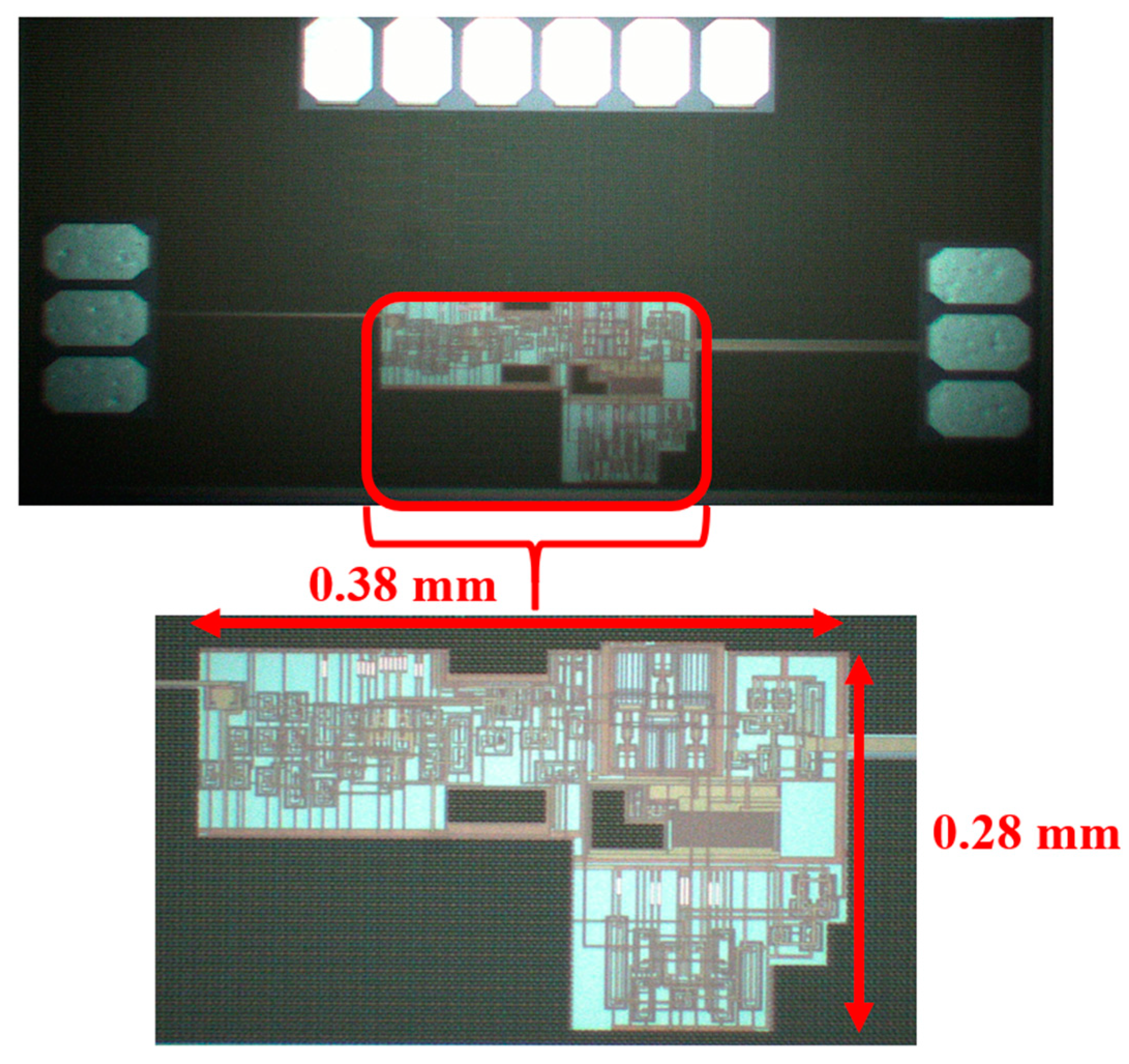
A microphotograph of the manufactured chip is given in
Figure 7. The core area measures 0.1 mm
2. Measurement results are given in
Section 5.
5. Results
During experimentations, as no PRBS generator was available in the lab, we used different input data sequences such as: ‘01’, ‘0011’, and ‘00001111’. An overview of the realized test bench is presented in
Figure 8.
Vctrl RO allows for precise locking to the target frequency whereas Vctrl inj controls the injection signal strength sent into the ring oscillator.
The recovered output clock signal is then connected to a splitter which separates into a spectrum analyzer and an oscilloscope.
5.1. Spectrum Analysis
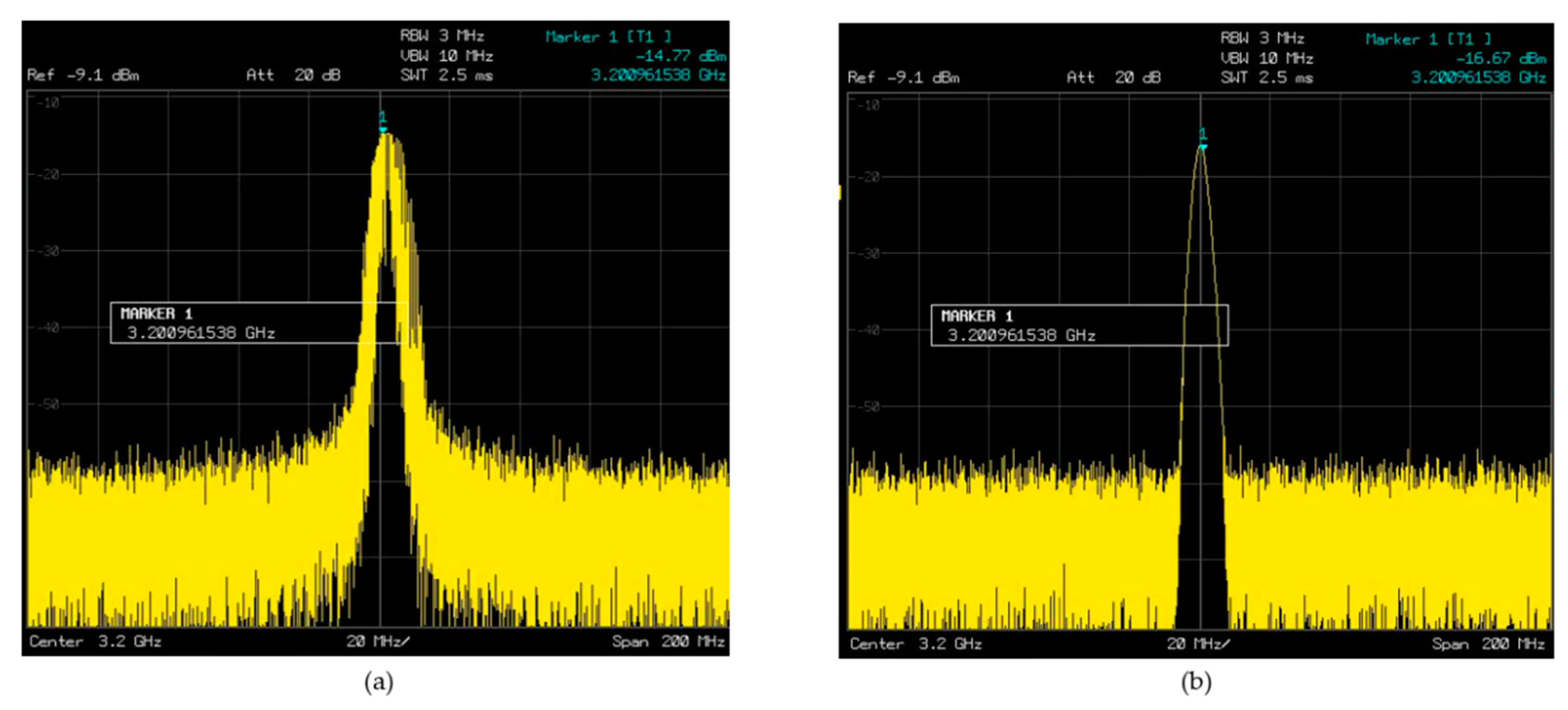
Figure 9 gives the comparison of the measured spectrum without and with injection locking at the target frequency of 3.2 GHz.
To give a fair comparison of the different spectrums, the same Resolution Bandwidth (RBW) is applied for both. By direct visual analysis,
Figure 9a shows a spectrum much more degraded than
Figure 9b. This result highlights the benefits brought by the synchronization by injection on the PLL circuit.
Further analyses have also been conducted in order to determine the impact of the injection strength on the synchronization range. Thus, for the whole control range, Vctrl inj = 0 V and Vctrl inj = 1.8 V, the corresponding synchronization range is around 150 MHz and 400 MHz, respectively.
To confirm the assumption given in the introduction concerning the phase noise and jitter improvements thanks to the injection locking, the next subsections address our resultant measures.
5.2. Phase Noise Analysis
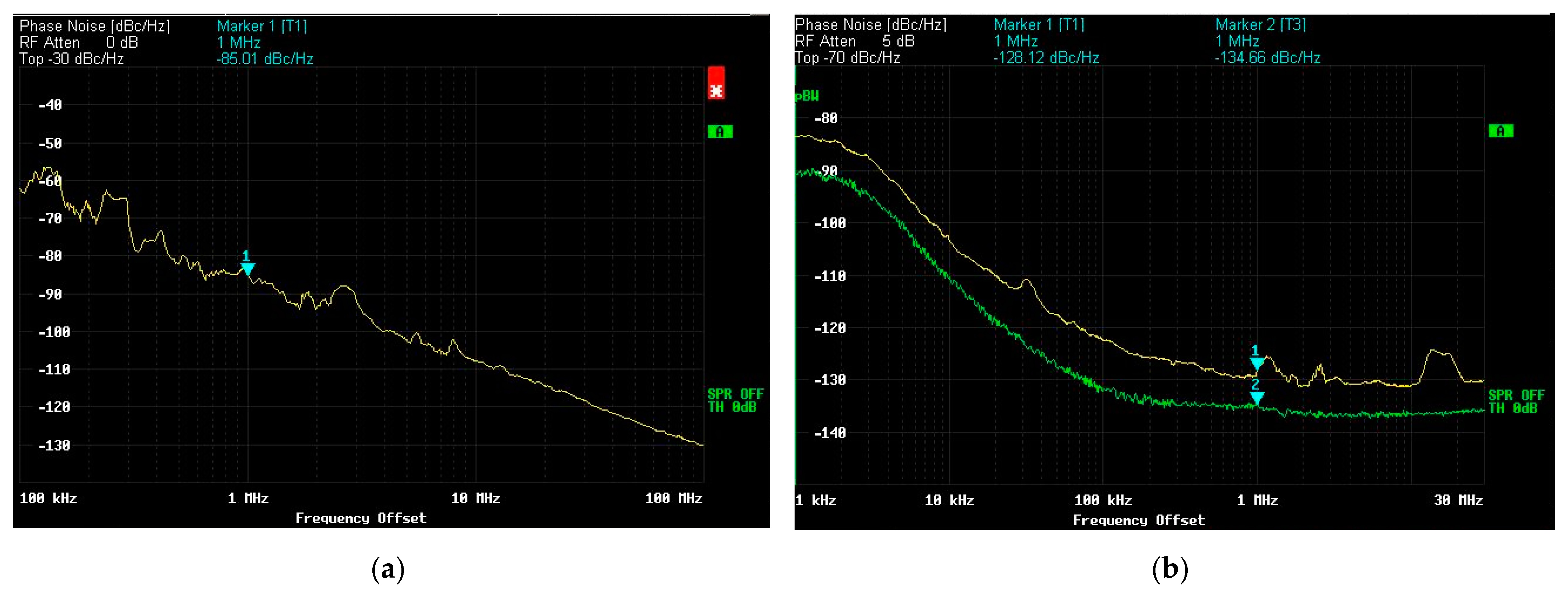
The next measurements illustrated in
Figure 10a show the phase noise without injection locking.
Figure 10b compares the respective phase noise of the input data signal (green curve) vs. the output PLL (yellow curve).
Figure 10a exhibits a phase noise without injection locking of −85 dBc/Hz at 1 MHz from the carrier frequency. When the PLL is synchronized by injection, the phase noise reaches −128.1 dBc/Hz at 1 MHz, which leads to an improvement of 43 dB. Moreover, knowing that our injection locking process is realized at the second harmonic, the phase noise recopy of the output signal should achieve a 6 dB difference, which corresponds to 20 logs (2).
Figure 10b gives the phase noise of the input data signal (green curve) of −134.7 dBc/Hz at 1 MHz, 6 dB lower than the output, which corroborates our expectations.
As shown in
Figure 10b some perturbations appear around the 1.2 MHz and 15 MHz deltas from the carrier frequency. After careful investigation, our conclusions led us to noise sources brought by the surrounding instrumentations in the lab.
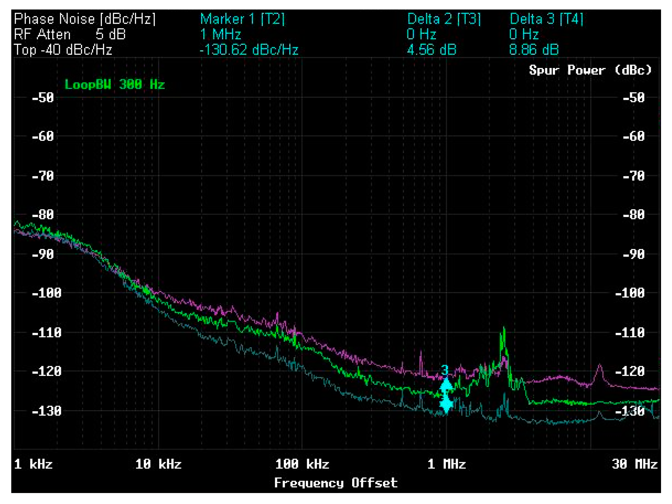
A 400 MHz of PLL capture range at the maximum injection strength was also measured. Additional phase noise measurements were realized to check if the injection locking process still operates correctly at the lower and upper edges of the capture range of the PLL.
Figure 11 illustrates this.
Results of
Figure 11 demonstrate a phase noise of −130.6 dBc/Hz at 1 MHz of the carrier frequency in the middle of the capture range (blue curve). A phase noise of −121.7 dBc/Hz (pink curve) and −126.6 dBc/Hz both at 1 MHz (green curve) at the lower and upper edges were measured, respectively. Even if those results still suggest phase noise improvements when the PLL remains under injection locking, our observations support the conclusion concerning the impact of the influence of the synchronization range on phase noise performance.
5.3. Jitter Analysis
The determination of the jitterrms is a crucial step in HSSL transceiver systems. One method widely used for its measurement is the eye diagram analysis, where the wider the eye is opened, the cleaner the obtained signal is. This parameter may either be expressed in the standard time-related unit or Unit Interval (UI).
As for spectrum measurement, we begin our approach by comparing the eye diagrams of the PLL without synchronization by injection and then under injection.
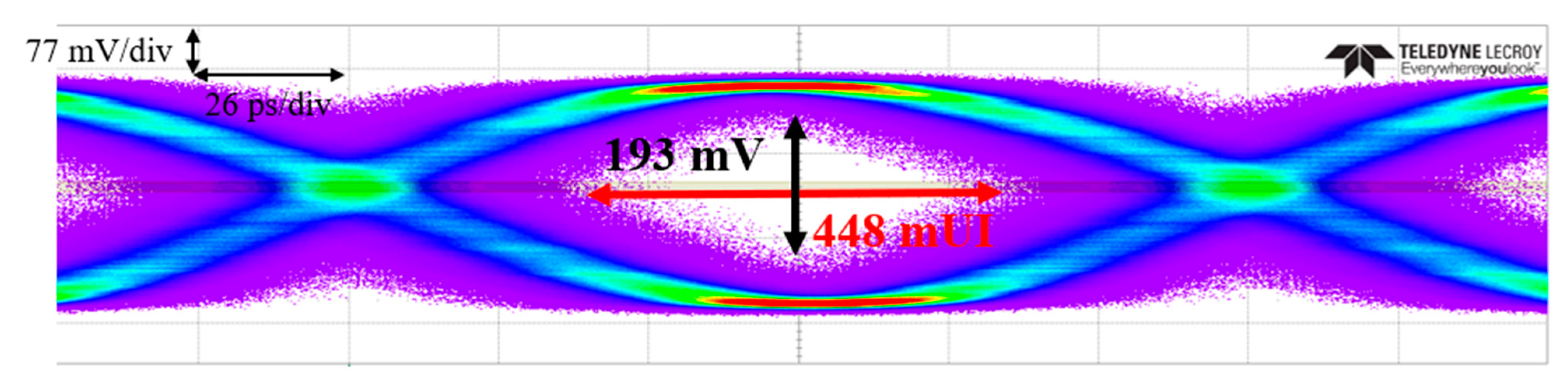
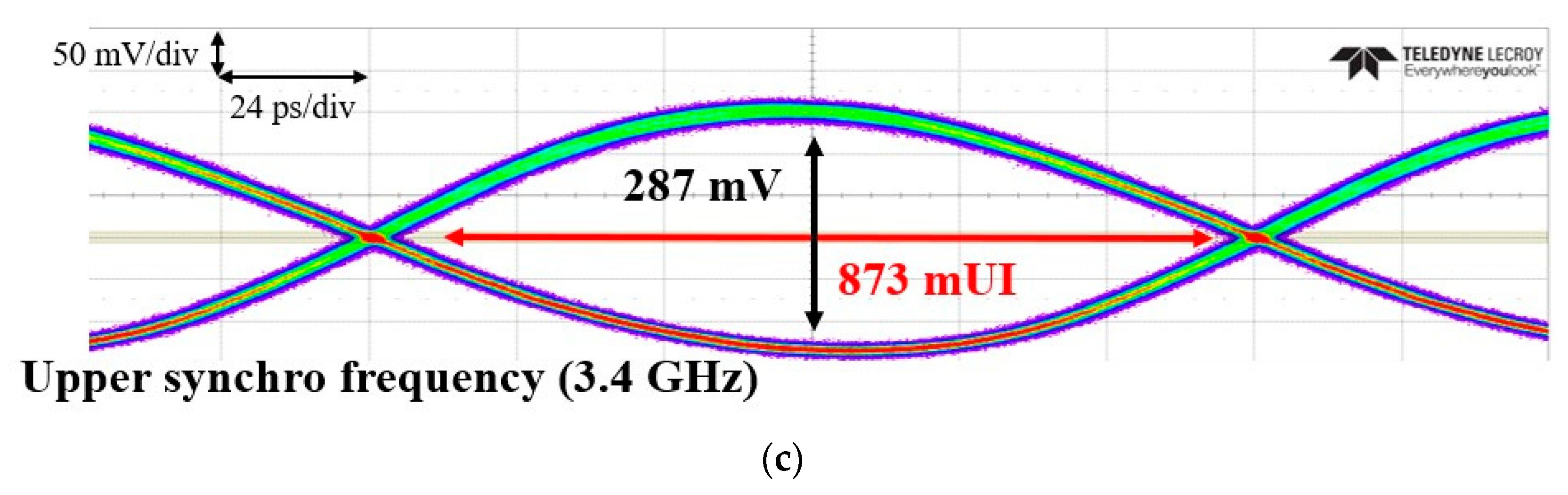
Figure 12 illustrates the eye diagram of the PLL circuit at 3.2 GHz.
The recovered eye gives an opening of 193 mV by 448 mUI. The measured jitterrms indicates 29.7 mUI.
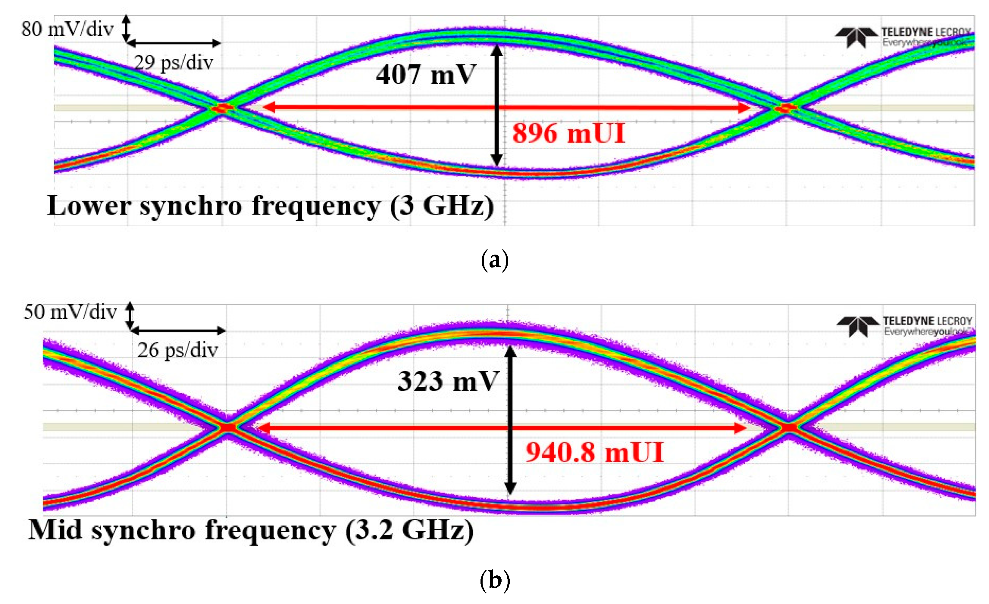
As previously demonstrated, we know that the injection locking process greatly improves the phase noise. As per the previous phase noise analysis, the corresponding eye diagrams at the same locations in the capture range are studied. Results are illustrated in
Figure 13.
The measurements indicate a jitterrms of 9.3 mUI at the lower edge capture range. At the initial target frequency, i.e., 3.2 GHz, a jitterrms of 6.4 mUI is achieved. At the upper capture range, a jitterrms of 9.5 mUI is measured. This leads to two observations: First, even if the eye opening widens while the frequency decreases, the optimal horizontal eye opening and jitterrms happen at the target frequency, that is to say, at the middle of the capture range. Secondly, even if jitter performance changes within the capture range, measurements still prove its efficiency by greatly enhancing its performance when compared to the eye diagram of the PLL without synchronization by injection.
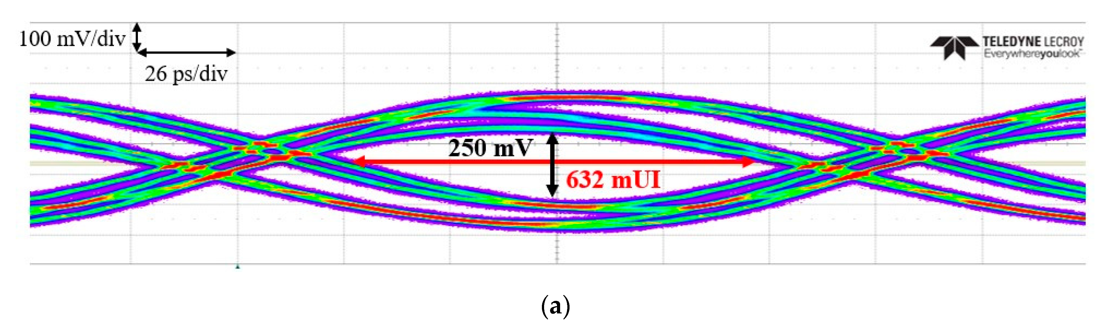
The results obtained so far have been measured for synchronization by injection at the second harmonic. For the input data, this corresponds to a bit pattern of ‘10’. To further pursue the analyses, additional measurements were conducted to analyze the circuit with longer bit sequences.
Figure 14a exposes the case of an input data sequence of ‘0011’, whereas
Figure 14b illustrates the case of ‘00001111’.
With longer bit sequences (
Figure 14a,b), the respective jitter
rms performances show 48.3 mUI and 58.2 mUI, respectively.
Indeed, additional measures showed that without the use of a PLL, the injection-locked ring oscillator standalone could not achieve such injection locking at these longer runlengths.
This section highlights the huge benefit of the synchronization by injection on ring oscillators while displaying an extremely low surface area. The next section is focused on the discussion and comparison of those measurements with similar state-of-the-art works.
6. Discussion
Table 2 gives a comparison of our study as opposed to the best state-of-the-art studies in terms of jitter, consumption, and surface area. The comparison is focused on CMOS technology operating at an equivalent frequency.
As
Table 2 shows, our work has a surface area of 0.1 mm
2. To give a fair comparison, we have calculated a parameter named
Normalized Surface, as [
23] has already introduced.
In addition to the total surface area, this
Normalized Surface also considers the technology node. According to
Table 2, our circuit shows the best
Normalized Surface performance.
Table 2 states a total power consumption of 34.6 mW for this work. The comparison to the other state-of-the-art studies shows a noticeable overconsumption. As the FoM
jitter is calculated from the total consumption, our work appears in the last position due to this overconsumption. Nevertheless, it is still important to point out that the work presented here constitutes a proof-of-concept. Thus, in the final circuit, the buffers, which are responsible for this overconsumption, will be deleted. This will translate to a 50% power savings which will drastically enhance the calculated FoM.
Moreover, as the 180 nm technology approaches its maximum operating frequency, many buffers are used only to compensate and straighten the signals. Reducing the technological node would obviate the presence of the buffer which would also further reduce the surface area.
Nevertheless, this consumption difference can be explained by two reasons. The first arises from the fact that the operating frequency of our work (3.2 GHz) appears close to the maximum achievable in the used technology and so explains the need for a higher consumption to ensure a correct operation. In the final version realized in a 28 nm FDSOI technology, the overall circuit consumption is divided by more than two.
The second cause justifying this overconsumption stems from the particular optimization layout method adopted in our circuit called the Enclosed Layout Transistor (ELT). As [
16,
17] point out, this principle employs a triple well and leads to an overconsumption of the circuit. As the power consumption was not chosen as a parameter to optimize, we decided to optimize the circuit hardening. Indeed, this
ELT remains on the principle of surrounding the whole circuit to prevent it from environmental assaults.
It is still quite interesting to note that our circuit has the widest operating frequency with 4 GHz versus the circuits in the state-of-the-art studies.
The comparisons shown in
Table 2 also demonstrate a similar jitter
rms of our work when compared to the rest of the studies.
Even if our work consumes the most power, the surface area occupied is, on contrary, the best of all of the state-of-the-art studies. As explained earlier, the
Normalized surface parameter allows a fair comparison between all the technology nodes. Even if [
18] and [
20] are substantially close to our work, the best normalized surface area still goes to our circuit. The
ELT technique employed, which also implies a higher surface area, is neglected in other works versus ours since our architecture does not require the implementation of any inductor, charge pump, or frequency divider which represent the usual elements in classic PLL circuits.
7. Conclusions
This work targets an industrial application dedicated for use in observation satellites. In the real-world context, companies expect to answer many constraints such as the size, weight, power consumption, operating frequency, etc., therefore, we chose to focus our optimizations on miniaturization and robustness as the main parameters of the circuit. The optimization of those parameters implies huge benefits in terms of weight.
In addition, the special design technique called the Enclosed Layout Transistor method has also been detailed. Even if this ELT technique requires a larger area than necessary, it significantly hardens the circuit to the extremely harsh space environment.
An injection-locked PLL circuit operating at the target frequency of 3.2 GHz with a 400 MHz bandwidth for a clock recovery application and dedicated to a space environment is presented. The appeal of the PLL circuit over the ring oscillator stand-alone has proven its usefulness by introducing a synchronization range, allowing for the maintenance of the lock of the PLL for a long series of identical bits.
The injection-locking mechanism has also indicated its efficiency by showing its phase noise (up to 43 dB) and jitter (80%) improvements.
To summarize, since the final application targets a clock recovery application dedicated to being implemented on satellites, the surface area occupied represented the very first parameter to optimize. As the comparison to other state-of-the-art studies showed, our work offers the lowest normalized surface area of 3.08, while exposing a jitterrms of 6.4 mUI.
Knowing that the injection locking process greatly upgrades jitter and phase noise performances, it appears that an optimized injection timing would improve those performances once again. Concerning the overall power consumption, most of the overconsumption comes from buffers devoted to measurements.
Author Contributions
Conceptualization, D.V., M.P., V.L., E.M., F.M. and J.-B.B.; methodology, D.V. and J.-B.B.; software, D.V.; validation, D.V., M.P., V.L., E.M. and J.-B.B.; formal analysis, D.V. and J.-B.B.; investigation, D.V. and J.-B.B.; resources, M.P., V.L., E.M., F.M. and J.-B.B.; data curation, M.P., V.L., E.M., F.M. and J.-B.B.; writing—original draft preparation, D.V.; writing—review and editing, D.V. and J.-B.B.; supervision, M.P., V.L. and J.-B.B.; project administration, M.P., V.L., E.M., F.M.; funding acquisition, M.P., V.L., E.M., F.M. and J.-B.B. All authors have read and agreed to the published version of the manuscript.
Funding
This research received no external funding.
Institutional Review Board Statement
Not applicable.
Informed Consent Statement
Not applicable.
Conflicts of Interest
The authors declare no conflict of interest.
References
- Chu, A.; Deo, N.; Ahmad, W.; Tormanen, M.; Sjoland, H.; Anh, C. An ultra-low power charge-pump PLL with high temperature stability in 130 nm CMOS. In Proceedings of the 2015 IEEE 13th International New Circuits and Systems Conference (NEWCAS), Grenoble, France, 7–10 June 2015; pp. 1–4. [Google Scholar] [CrossRef]
- Kanemaru, N.; Ikeda, S.; Kamimura, T.; Lee, S.; Tanoi, S.; Ito, H.; Ishihara, N.; Masu, K. A ring-VCO-based injection-locked frequency multiplier using a new pulse generation technique in 65 nm CMOS. In Proceedings of the 2011 International SoC Design Conference, Jeju, Korea, 17–18 November 2011; pp. 32–35. [Google Scholar] [CrossRef]
- Lu, L.-H.; Chien, J.-C. A wide-band CMOS injection-locked ring oscillator. IEEE Microw. Wirel. Components Lett. 2005, 15, 676–678. [Google Scholar] [CrossRef]
- Abdulaziz, M.; Forsberg, T.; Tormanen, M.; Sjoland, H. A 10-mW mm-Wave Phase-Locked Loop with Improved Lock Time in 28-nm FD-SOI CMOS. IEEE Trans. Microw. Theory Tech. 2019, 67, 1588–1600. [Google Scholar] [CrossRef] [Green Version]
- Lee, J.; Wang, H. Study of Subharmonically Injection-Locked PLLs. IEEE J. Solid-State Circuits 2009, 44, 1539–1553. [Google Scholar] [CrossRef]
- Adler, R. A study of locking phenomena in oscillators. Proc. IEEE 1973, 61, 1380–1385. [Google Scholar] [CrossRef]
- Razavi, B. A study of injection locking and pulling in oscillators. IEEE J. Solid-State Circuits 2004, 39, 1415–1424. [Google Scholar] [CrossRef]
- Lapuyade, H.; Mazouffre, O.; Goumballa, B.; Pignol, M.; Malou, F.; Neveu, C.; Pouget, V.; Deval, Y.; Begueret, J.B. A Heavy-Ion Tolerant Clock and Data Recovery Circuit for Satellite Embedded High-Speed Data Links. IEEE Trans. Nucl. Sci. 2007, 54, 2080–2085. [Google Scholar] [CrossRef]
- Piccin, Y.; Lapuyade, H.; Deval, Y.; Morche, C.; Seyler, J.-Y.; Goutti, F. Radiation-Hardening Technique for Voltage Reference Circuit in a Standard 130 nm CMOS Technology. IEEE Trans. Nucl. Sci. 2014, 61, 967–974. [Google Scholar] [CrossRef]
- Lai, X.; Roychowdhury, J. Analytical equations for predicting injection locking in LC and ring oscillators. In Proceedings of the IEEE 2005 Custom Integrated Circuits Conference, San Jose, CA, USA, 21 September 2005; pp. 454–457. [Google Scholar] [CrossRef]
- Gangasani, G.R.; Kinget, P.R. Time-domain model for injection locking in nonharmonic oscillators. IEEE Trans. Circuits Syst. I Regul. Pap. 2008, 55, 1648–1658. [Google Scholar] [CrossRef]
- Mesgarzadeh, B.; Alvandpour, A. A Study of Injection Locking in Ring Oscillators. In Proceedings of the 2005 IEEE International Symposium on Circuits and Systems, Kobe, Japan, 23–26 May 2005; pp. 5465–5468. [Google Scholar] [CrossRef]
- Bhansali, P.; Roychowdhury, J. Gen-Adler: The Generalized Adler’s Equation for Injection Locking Analysis in Oscillators. In Proceedings of the 2009 Asia and South Pacific Design Automation Conference, Yokohama, Japan, 19–22 January 2009. [Google Scholar] [CrossRef] [Green Version]
- Razavi, B. The Ring Oscillator [A Circuit for All Seasons]. IEEE Solid-State Circuits Mag. 2019, 11, 10–81. [Google Scholar] [CrossRef]
- Schmidt, L.; Rein, H.-M. New high-speed bipolar XOR gate with absolutely symmetrical circuit configuration. Electron. Lett. 1990, 26, 430–431. [Google Scholar] [CrossRef]
- Franciscatto, G.; Geukensb, E.; Thysa, G.; Redanta, S.; Geertsb, Y.; Fossionc, M.; Van Esbeenc, A. DARE180X: A 0.18μm mixed-signal radiation-hardened library for low-power applications. In Proceedings of the 5th International Workshop on Analogue and Mixed-Signal Integrated Circuits for Space Applications, Zurich, Switzerland, 30 June 2014; Available online: https://indico.cern.ch/event/277669/session/5/contribution/27 (accessed on 3 October 2022).
- Anelli, G.; Campbell, M.; Delmastro, M.; Faccio, F.; Floria, S.; Giraldo, A.; Heijne, E.; Jarron, P.; Kloukinas, K.; Marchioro, A.; et al. Radiation tolerant VLSI circuits in standard deep submicron CMOS technologies for the LHC experiments: Practical design aspects. IEEE Trans. Nucl. Sci. 1999, 46, 1690–1696. [Google Scholar] [CrossRef] [Green Version]
- Chou, M.-H.; Liu, S.-I. A 2.4-GHz Area-Efficient and Fast-Locking Subharmonically Injection-Locked Type-I PLL. IEEE Trans. Very Large Scale Integr. VLSI Syst. 2020, 28, 2474–2478. [Google Scholar] [CrossRef]
- He, Y.; Heuvel, J.V.D.; Mateman, P.; Allebes, E.; Traferro, S.; Dijkhuis, J.; Bunsen, K.; Vis, P.; Breeschoten, A.; Liu, Y.-H.; et al. An Injection-Locked Ring-Oscillator-Based Fractional-N Digital PLL Supporting BLE Frequency Modulation. IEEE J. Solid-State Circuits 2022, 57, 1765–1775. [Google Scholar] [CrossRef]
- Xi, N.; Lin, F.; Ye, T. A Low-Spur and Intrinsically Aligned IL-PLL with Self-Feedback Injection Locked RO and Pseudo-Random Injection Locked Technique. IEEE Trans. Circuits Syst. I Regul. Pap. 2020, 67, 1358–1367. [Google Scholar] [CrossRef]
- Phan, K.T.; Chao, Y.; Luong, H.C. A 1.92GHz-3.84GHz 0.74ps-1.09ps-Jitter Inductor-less Injection-Locked Frequency Synthesizer with Automatic Frequency Selection and Timing Alignment. In Proceedings of the 2021 IEEE Asian Solid-State Circuits Conference (A-SSCC), Busan, Korea, 7–10 November 2021; pp. 1–3. [Google Scholar] [CrossRef]
- Jin, X.; Park, W.; Kang, D.-S.; Ko, Y.; Kwon, K.-W.; Chun, J.-H. A 4-GHz Sub-Harmonically Injection-Locked Phase-Locked Loop with Self-Calibrated Injection Timing and Pulsewidth. IEEE J. Solid-State Circuits 2020, 55, 2724–2733. [Google Scholar] [CrossRef]
- Gaidioz, D. Ultra-Low Power Frequency Synthesizer for Internet-of-Things Applications in 28 nm FD-SOI Technology. 7 September 2021. Available online: https://tel.archives-ouvertes.fr/tel-03336167 (accessed on 3 October 2022).
Figure 1.
Full 3.2 GHz injection-locked PLL architecture.
Figure 1.
Full 3.2 GHz injection-locked PLL architecture.
Figure 2.
Pulse generator schematic.
Figure 2.
Pulse generator schematic.
Figure 3.
Pulse generator chronogram.
Figure 3.
Pulse generator chronogram.
Figure 4.
V/I converter schematic.
Figure 4.
V/I converter schematic.
Figure 5.
Ring oscillator schematic.
Figure 5.
Ring oscillator schematic.
Figure 6.
XOR-based fully symmetrical phase detector.
Figure 6.
XOR-based fully symmetrical phase detector.
Figure 7.
Microphotograph of the circuit.
Figure 7.
Microphotograph of the circuit.
Figure 8.
Schematic of the test bench.
Figure 8.
Schematic of the test bench.
Figure 9.
Comparison of the PLL spectrum (a) without injection locking and (b) with injection locking.
Figure 9.
Comparison of the PLL spectrum (a) without injection locking and (b) with injection locking.
Figure 10.
Phase noise (a) without injection locking; (b) comparison of the PLL under injection locking (yellow curve) vs. the input data signal (green curve).
Figure 10.
Phase noise (a) without injection locking; (b) comparison of the PLL under injection locking (yellow curve) vs. the input data signal (green curve).
Figure 11.
Phase noise comparison at the lower edge (pink curve), the middle range (blue curve), and the upper edge (green curve) of the PLL’s capture range.
Figure 11.
Phase noise comparison at the lower edge (pink curve), the middle range (blue curve), and the upper edge (green curve) of the PLL’s capture range.
Figure 12.
Eye diagram of the PLL without synchronization by injection.
Figure 12.
Eye diagram of the PLL without synchronization by injection.
Figure 13.
Eye diagram comparison of the PLL synchronized by injection at the (a) lower, (b) mid-range, and (c) upper capture range.
Figure 13.
Eye diagram comparison of the PLL synchronized by injection at the (a) lower, (b) mid-range, and (c) upper capture range.
Figure 14.
Eye diagrams of the PLL synchronized by injection for an (a) ‘0011’ sequence and (b) ‘00001111’ sequence.
Figure 14.
Eye diagrams of the PLL synchronized by injection for an (a) ‘0011’ sequence and (b) ‘00001111’ sequence.
Table 1.
Summary of phase noise, jitter, and eye opening performances of the PLL without and with injection locking.
Table 1.
Summary of phase noise, jitter, and eye opening performances of the PLL without and with injection locking.
| | PLL without Injection | PLL with Injection |
|---|
| Lower Edge | Middle | Upper Edge |
|---|
| Operating frequency (GHz) | 3.2 | 3 | 3.2 | 3.4 |
| Phase noise (dBc/Hz at 1 MHz) | −85 | −121.7 | −130.6 | −126.6 |
| Jitterrms (mUI) | 29.7 | 9.3 | 6.4 | 9.5 |
| Power consumption (mW) | 30.8 | 34.6 |
Table 2.
Performance comparison to other state-of-the-art studies.
Table 2.
Performance comparison to other state-of-the-art studies.
| | This Work | [18]
TVLSI
2020 | [19]
JSSC
2022 | [20]
TCAS-I
2020 | [21]
ASSCC
2021 | [22]
JSSC
2020 |
|---|
| Technology (nm) | 180 | 45 | 40 | 180 | 65 | 28 |
| Operating frequency range (GHz) | 0.2–4.2 | 2.4 | 1.8–2.7 | 2.5 | 1.9–3.8 | 4 |
| Jitterrms (mUI) | 6.4 | 2.2 | 5.7 | 0.3 | 3.4 | 2.8 |
| Consumption (mW) | 34.6 | 5.6 | 2.76 | 6.1 | 4.3 | 11.4 |
| Surface (mm2) | 0.1 | 0.013 | 0.09 | 0.142 | 0.22 | 0.09 |
| Normalized surface (106) | 3.08 | 6.41 | 56.25 | 4.38 | 52.07 | 114.8 |
| FoMjitter | −217.6 | −233.3 | −229.1 | −250.6 | −234.7 | −232.5 |
| Publisher’s Note: MDPI stays neutral with regard to jurisdictional claims in published maps and institutional affiliations. |
© 2022 by the authors. Licensee MDPI, Basel, Switzerland. This article is an open access article distributed under the terms and conditions of the Creative Commons Attribution (CC BY) license (https://creativecommons.org/licenses/by/4.0/).


