Article

Performance Benchmarking of TFET and FinFET Digital Circuits from a Synthesis-Based Perspective

1
Instituto de Micro y Nanoelectrónica (IMNE), Universidad San Francisco de Quito (USFQ), Quito 170901, Ecuador
2
Department of Computer Engineering, Modeling, Electronics and Systems, University of Calabria, 87036 Rende, Italy
*
Author to whom correspondence should be addressed.
Submission received: 30 December 2021 / Revised: 28 January 2022 / Accepted: 30 January 2022 / Published: 18 February 2022

Abstract

:
Miniaturization and portable devices have reshaped the electronic device landscape, emphasizing the importance of high performance while maintaining energy efficiency to ensure long battery life. FinFET and Tunnel-FET technologies have emerged as attractive alternatives to overcome the limitations of supply voltage scaling for ultra-low power applications. This work compares the performance of 10 nm FinFET- and TFET-based digital circuits from basic logic gates up to an 8k gates low-power microprocessor. When compared with their FinFET-based counterparts, the TFET-based logic gates have lower leakage power when operated below 300 mV, show higher input capacitance, and exhibit a reduced propagation delay under different fan-in and fan-out conditions. Our comparative study was extended to the synthesis of an MSP-430 microprocessor through standard cell libraries built particularly for this work. It is demonstrated that the TFET-based synthesized circuits operating at ultra-low voltages achieve a higher performance in terms of speed at the cost of increased power consumption. When the speed requirements are relaxed, the TFET-based designs are the most energy-efficient alternative. It is concluded that the TFET is an optimal solution for ultra-low voltage design.

1. Introduction

The emergence of portable applications has ushered in the development of several compact electronics, including wireless sensor networks, Internet of Things devices, biomedical technologies, and wearable equipment. Most of these electronic devices of reduced size target energy efficiency since reducing the power consumption directly translates into a longer battery lifetime [1,2,3,4,5,6,7,8]. Supply voltage down-scaling is an effective method to achieve a minimum energy operation for relaxed-performance applications [9,10,11,12]. Therefore, ultra-low-power circuits can be achieved with an ultra-low-voltage (ULV) operation near the subthreshold region. Nevertheless, subthreshold operation implies an increased sensitivity in the variation of circuit parameters and an exponential increase in propagation delay [11,12]. The manufacturing process of the bulk CMOS technology has run into limitations, such as poor scalability, high leakage current, and short channel effects, despite the fact that the down-scaling of this technology has been the common solution to maintain an acceptable circuit performance [13,14].
Supply voltage reduction and the shrinking of technology nodes in the planar CMOS process result in drawbacks that no longer meet the energy efficiency and performance requirements of modern portable devices. Alternative device concepts based on different operating principles and semiconductor materials are required to deal with the above challenges [15]. The FinFET device has been proposed as an alternative to bulk CMOS technology nodes below 32 nm thanks to its superior scalability, lower gate leakage current, and a better control over short-channel effects [16,17,18]. However, FinFET and bulk CMOS devices share thermionic emission as a main mechanism of conduction, which limits their subthreshold slope (SS) to 60 mV/dec at room temperature [19,20,21].
The Tunnel Field-Effect Transistor (TFET) is a device capable of outperforming conventional MOSFET designs such as bulk CMOS and FinFET devices [21,22,23]. The main conduction mechanism of this device is determined by the band-to-band tunneling at the source-channel; therefore, the SS of the TFET is able to achieve a high-efficiency ultra-low-voltage computation due to a sub-60-mv/dec operation [21,22,23,24,25]. The lower SS of the TFET produces a relatively large on-current at a lower supply voltage, a reduced leakage, and an enhanced low-voltage, as a result of thermionic emission not being involved in this device [26,27,28]. The TFET is based on III-V heterojunction structures which produces an asymmetric device with a unidirectional current, and is the cause of the p-type TFET having an on-current four times smaller than its n-type counterpart [21,23]. In addition, the large capacitance of the TFET caused by its source-channel barrier induces voltage spikes during circuit switching, which can increase power consumption [23,26].
This section introduces the tendency of modern portable devices to require an energy-efficient performance, the limitations of the most used techniques such as low-voltage design and miniaturization on the planar CMOS process, as well as two alternative devices, the FinFET and TFET, each with different characteristics and advantages at a ULV operation. In this work, an extensive comparison of 10 nm FinFET- and TFET devices is presented from basic standard cells up to the synthesis of a low-power 8K gates microprocessor. As the main contribution, it is demonstrated that under a sizing criterion that optimizes the noise margin of the standard cell libraries at low-voltage operation, a TFET-based MSP-430 microprocessor presents a clear trade-off between performance and power consumption. In particular, it is able to achieve a 13.0× faster speed of operation by consuming 6.7× more power than a FinFET-based MSP microprocessor. Additionally, a TFET-based MSP microprocessor synthesized for low-power consumption achieved 34.8% less power than a FinFET-based MSP microprocessor at supply voltages as low as 200 mV.
The rest of this article is organized as follows: Section 2 discusses the device specification and sizing methodology, Section 3 shows the characterization and synthesis results, and Section 4 concludes the work.

2. Methodology

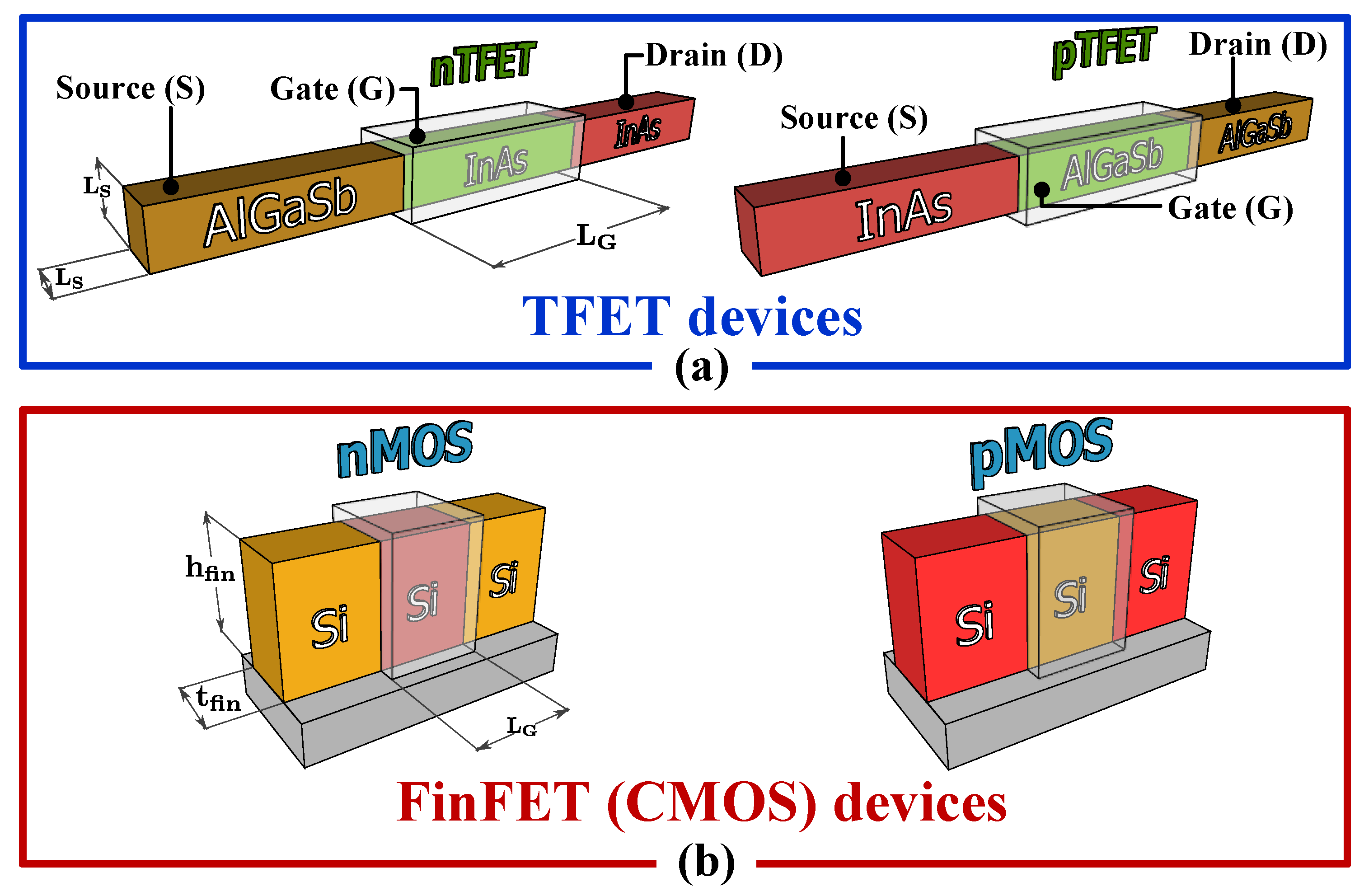
2.1. Device Specification

Figure 1 shows the physical structure of the (a) TFET and (b) FinFET devices used in this work. The FinFET devices have a fin height ( h f i n ) of 21 nm, a fin width ( t f i n ) of 8 nm, an L G of 14 nm, and an equivalent oxide thickness ( E O T ) of 0.88 nm. The TFET devices have a square cross-section ( L S ) with a side of 7 nm, a gate length ( L G ) of 20 nm, and E O T of 1 nm. The FinFET devices used in this work are described by the Predictive Technology Models of Multi-Gate transistors (PTM-MG) of the 10 nm node, which are available through spice models in [29]. The FinFET PTM includes two versions: high-performance (HP) and low-standby-power (LSTP). The latter will be used since this work focuses on the ULV range. The TFETs are described through dense Look-Up Tables (LUTs) for I D , C G S , and C G D as a function of V G S and V D S contained in Verilog-A files. The TFET models (i.e., LUTs) are fully described in [21,23], where the TCAD simulator Sentaurus Device was used to reproduce full-quantum simulations of the AlGaSb/InAs heterostructure of the device.
The superior SS of the TFET can be exploited in two different ways: (1) equalizing the threshold voltage of the TFET to that of the FinFET in order to obtain a lower off-current and lesser static energy dissipation, or (2) by setting the same off-current in both devices so that the TFET is able to achieve a higher on-current at lower supply voltages [23]. This last method focuses on the ULV domain and, therefore, is considered throughout this work. Accordingly, this calibration can be visualized in Figure 2 where the drain current and gate capacitance of the p-type and n-type versions of the FinFET and TFET devices are pictured. The off-current of the p-type and n-type TFET devices have been calibrated, respectively, to 1.30 pA and 1.49 pA, while their extrinsic capacitance has been set to 30 aF. Note that the superior SS of the TFET is evident since it can achieve a higher on-current than the FinFET at supply voltages lower than 400 mV. The TFET device has an inherent asymmetry due to its AlGaSb/InAs physical heterojuntion, in contrast to the symmetric Si structure of the FinFET, making the on-current of the p-type TFET almost four times smaller than its n-type counterpart. This asymmetry can also be appreciated in the I D vs. V D S plot where raising the V G S voltage on the FinFET produces a constant increase in drain current. This is not the case for the TFET device, where the gain in drain current slowly decreases when applying more V G S voltage due to the decreasing SS. It can also be seen that the gate capacitance of the TFET devices at ULV is larger than the FinFET devices, with the p-type TFET being strongly asymmetric and larger than its n-type counterpart.

2.2. Sizing Methodology

The inherent asymmetry of the TFET device, as made evident in the previous subsection, causes the n-type TFET to drive up to 4-times more on-current than the p-type. This characteristic can be addressed through a sizing methodology where the p- and n-type devices in the Pull-Up (PUN) and Pull-Down (PDN) Networks of a logic gate are assigned different sizes so that both networks drive the same current, optimizing the noise margin of the gate [21,23]. Figure 3 shows the effect of the sizing methodology on the noise margin of the butterfly plot of TFET- and FinFET-based inverters at 300 mV with W P / W N ratios of 3/1 and 1/1, respectively. Note that the ratios are discrete, since multipliers are used to manipulate the sizes of the TFET and FinFET devices due to their tridimensional nature. While a sizing ratio of 1/1 is enough to optimize the noise margin in the symmetric FinFET device, the asymmetric TFET requires a larger PUN since the p-type TFET drives a smaller on-current.
Table 1 shows the W P / W N ratios of an inverter, NOR2, NOR3, NAND2, and NAND3 gates after the sizing process, considering a supply voltage V D D of 300 mV. The NOR and NAND gates were sized on a worst-case metric acting as an inverter (i.e., with their inputs short-circuited). It can be observed that FinFET-based gates have smaller sizes than their TFET-based counterparts due to the symmetric nature of the former. Table 1 also shows that the INV and NOR gates have a smaller size than the NAND gates under this sizing procedure. Table 2 shows the noise margin as a percentage of half the supply voltage for different TFET- and FinFET-based logic gates at 200, 300, and 400 mV after the sizing process. It is clear that the selected sizing method ensures a similar noise margin for both TFET and FinFET versions of the same logic gate at 300 mV. A change in the supply voltage causes a reduction in the noise margin of the TFET-based cells due to the asymmetry of this device, in contrast to what happens in the FinFET-based counterparts, where the robustness of the cells is maintained in a better manner when the supply voltage is changed. It is worth mentioning that most of the noise margins of the logic gates are above 100 mV, which is the lower bound value suggested to ensure reliable operation. Although logic gates operating at a voltage supply of 200 mV present noise margins around such a lower bound value (i.e., 100 mV), suggesting that logic decisions could be affected, the noise margin can be improved by operating at lower temperatures (below room temperature).
Three sets of chains were created to study the effects of the sizing scheme on their performance in terms of energy and propagation delay. The three chains implemented were 20 inverters (INV Chain), 20 interleaved NAND2–NOR2 gates, and 20 interleaved NAND3–NOR3 gates acting as inverters with their energy–delay plot over a supply voltage range of 300 mV to 500 mV, as pictured in Figure 4. The TFET-based implementations are, on average, 4.3× faster below 400 mV and 2.7× slower above this supply voltage while being 3.7× more energy consuming across the whole supply voltage range. Therefore, the selected sizing methodology on the TFET-based implementations optimizes the noise margin and improves the speed performance at ULV, albeit with higher energy consumption. It must also be noted that the two-input NAND–NOR chains have a better performance in terms of speed (2.8× and 3.8× for FinFET and TFET-based implementations, respectively) with a change in energy consumption of less than 10%, making this chain implementation more attractive than their three-input counterparts. The Energy–Delay Product (EDP) of these chains across the supply voltage is presented in Figure 5. The EDP is a useful figure-of-merit for studying the advantages of TFET-based circuits and the ULV range in which they can outperform other technologies (e.g., FinFET in this case) [13]. Figure 5 demonstrates that the TFET-based implementations present a smaller EDP than their FinFET-based counterparts at supply voltages below 330mV. Therefore, a synthesis-driven exploration is considered for circuits operating around the sizing voltage (i.e., 300 mV).

3. Results and Discussion

Standard cell libraries containing TFET- and FinFET-based logic cells are characterized to achieve the synthesis of an MSP-430 microprocessor, as well as to compare the performance of the implementations using these devices. Synopsys SiliconSmart was used as the characterization tool for basic logic gates working with the TFET and FinFET transistor models described in Section 2. Synopsys Design Compiler was used to synthesize complex circuits from the generated standard cell libraries. Table 3 showcases the parameters used in the characterization process to produce the standard cell libraries. For the sake of accuracy, considering that the TFET devices we refer to in this assessment were characterized at room-temperature [21], we limited our study to 25 °C for supply voltages ranging from 200 to 500 mV. A pass-transistor D Flip-Flop topology with inverters acting as input and output buffers is used. To ensure robust designs, the synthesized architectures are mapped with logic cells possessing noise margins above 120 mV, since the sizing selected was carried out at 300 mV. A wide load capacitance and input slope range was selected to ensure characterization conditions appropriate for FinFET- and TFET-based logic gates.
The results in this section are divided into two parts, the Characterization Results in Section 3.1 and the Synthesis Results in Section 3.2. The three-input NAND and NOR gates on Table 3 are marked with an asterisk (*) to indicate that they will only be used in the Characterization Results section, since it was previously demonstrated that they do not offer an advantage over the two-input versions (refer to Figure 4). It must be highlighted that our synthesis-based early assessment was performed without considering layout parasitic effects in the simulations. This is because TFET is not a mature technology and the models used in this work do not consider an area description of these devices.

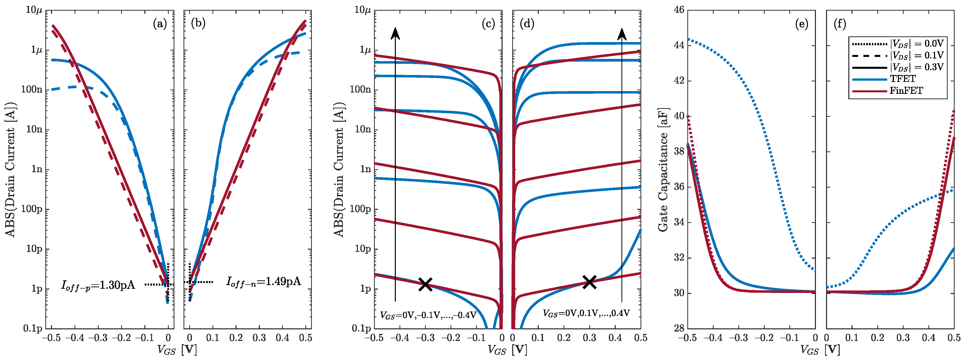
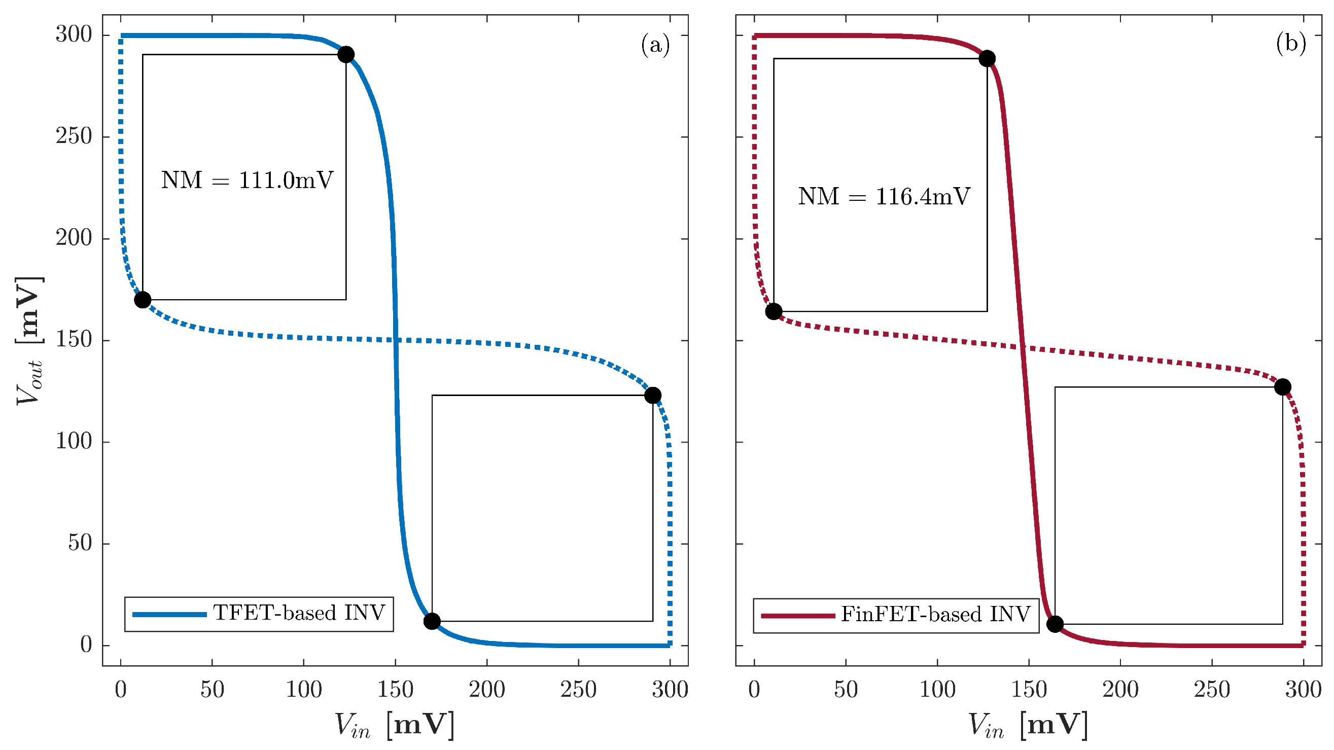
3.1. Characterization Results

Figure 6 shows the leakage power of TFET- and FinFET-based logic gates operating over a wide supply voltage range. The logic gates were separated into two groups: (a) the inverter, NOR2, and NOR3 gates, and (b) the D Flip-Flop, NAND2, and NAND3 gates. This distinction was made due to the logic gates in group (a) having smaller dimensions (i.e., smaller sizing, as explained in Section 2) than those in group (b). The difference between both groups of logic gates is caused by the sizing methodology and applies to both TFET- and FinFET-based implementations. From Figure 6a, as compared with FinFET-based logic gates, the TFET-based alternatives exhibit a decrease in leakage power of about 3%. In particular, for supply voltages below 400mV, the leakage power is reduced by about 18%. Above 400 mV, the TFET-based gates from group (a) and (b) consume, respectively, 5.4× and 9.8× more leakage power as compared with the FinFET-based counterparts.
The input capacitance of the characterized logic gates is listed on Table 4. The D Flip-Flop gate has two distinct inputs: (1) the CLK input and (2) the data (D) input, which are connected to a pass transistor and to a buffer, respectively. Table 4 demonstrates that similar-sized gates produce the same input capacitance (i.e., FinFET-based NOR2 and NOR3 or the DFF-D and INV gates), as well as the fact that the TFET-based alternatives always present a higher input capacitance value. Across every input of all the gates, the TFET-based versions have an input capacitance 2.9× larger than their FinFET-based counterparts.
Figure 7 shows the propagation delay of the main combinational logic gates (i.e., INV and NOR2) at supply voltages of (a,b) 300 mV and (c,d) 400 mV across a mesh of load capacitance and input slope values. In general, the TFET-based logic gates have lower propagation delay across extreme values of load capacitance and input slope, even at supply voltages as high as 400 mV. Moreover, TFET-based logic gates have a larger advantage in terms of speed performance at 300 mV than at 400 mV because of their steep SS at ULV. Note that Figure 7 indicates that the TFET-based implementations can reach a better propagation delay at 400 mV than their FinFET-based counterparts when the input and output conditions are the same for both devices. Nevertheless, it was shown that the TFET-based gates represent a higher input capacitance under the selected sizing methodology; therefore, large and complex designs might not exhibit this advantage over their FinFET-based counterparts at voltages higher than 300 mV.

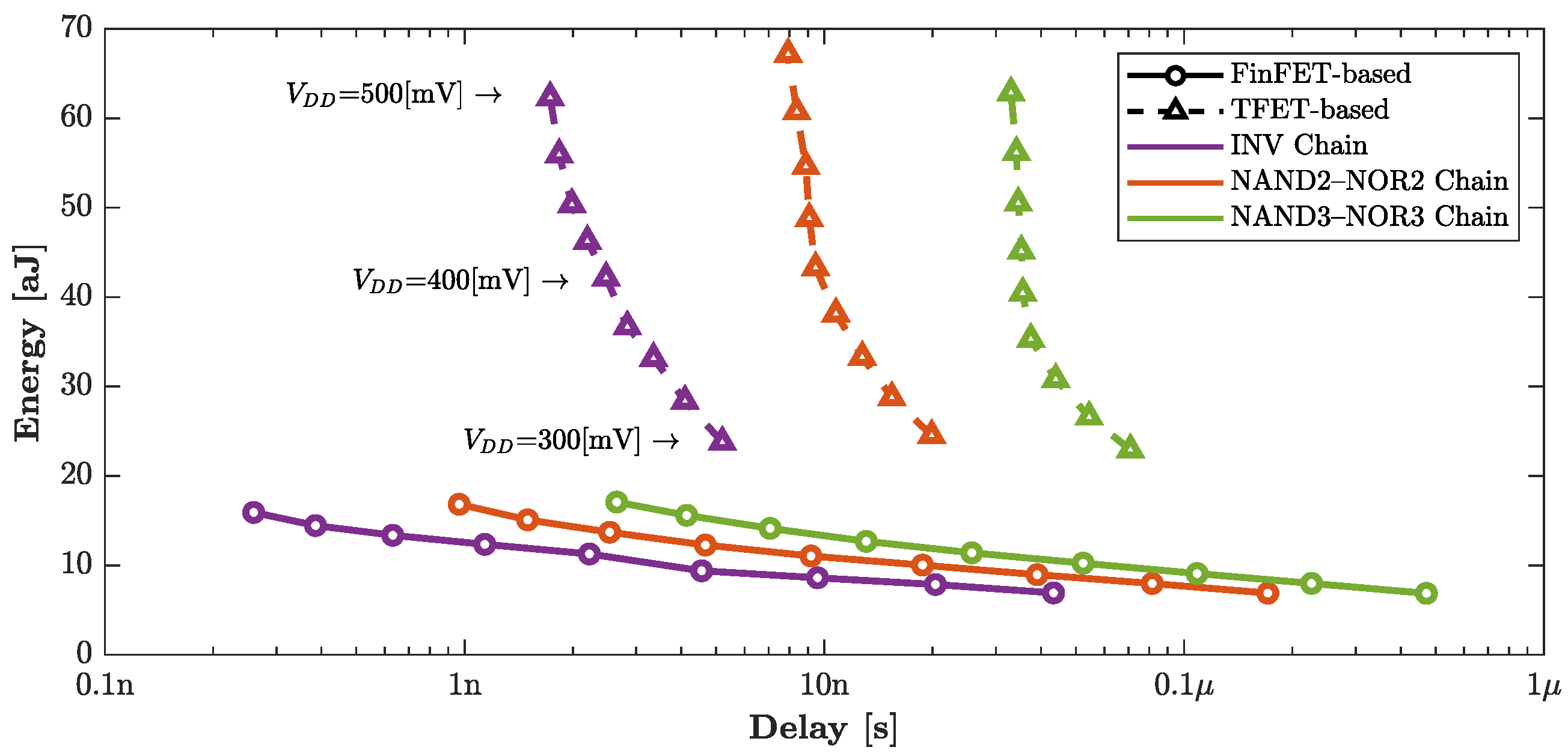
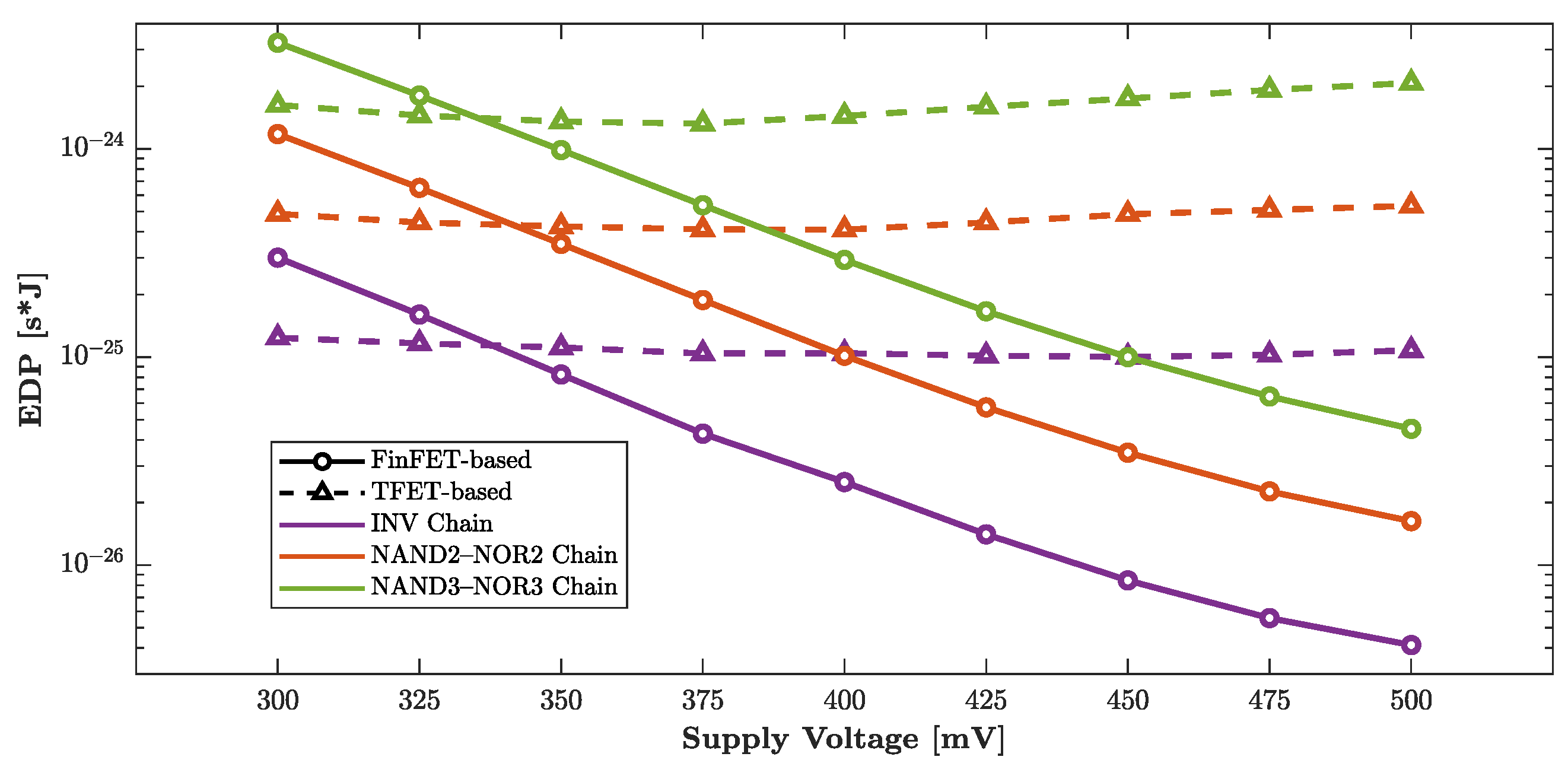
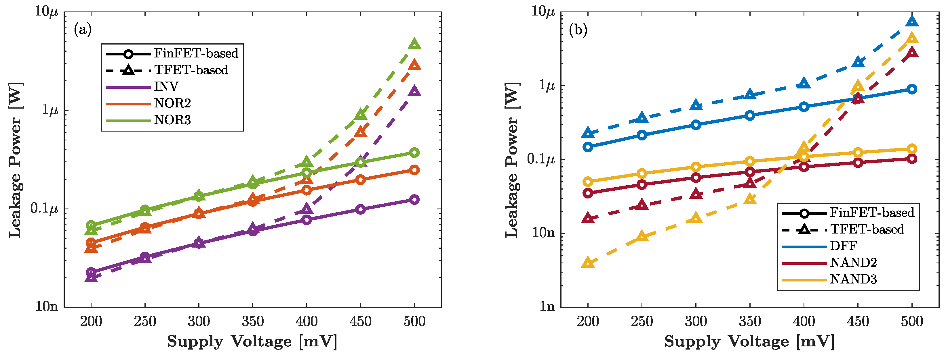
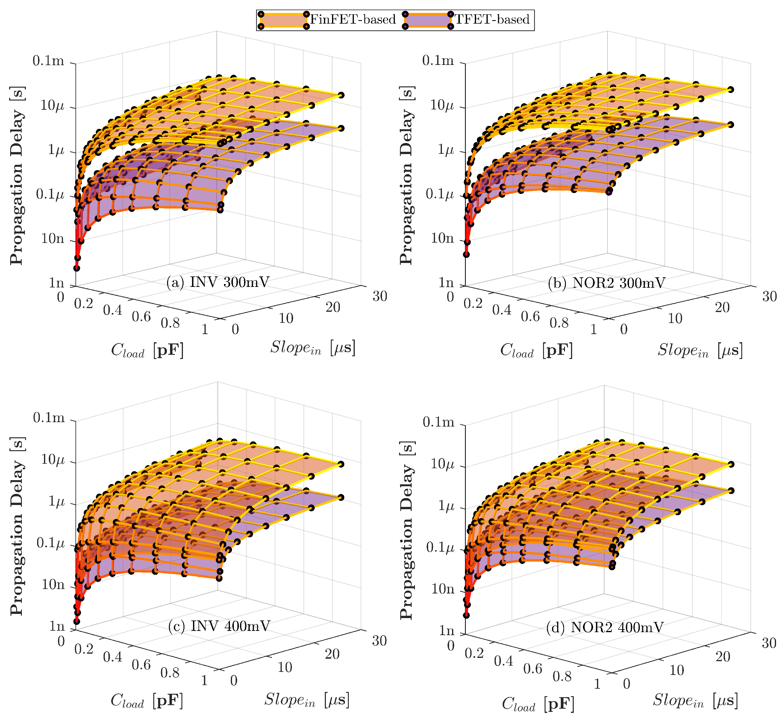
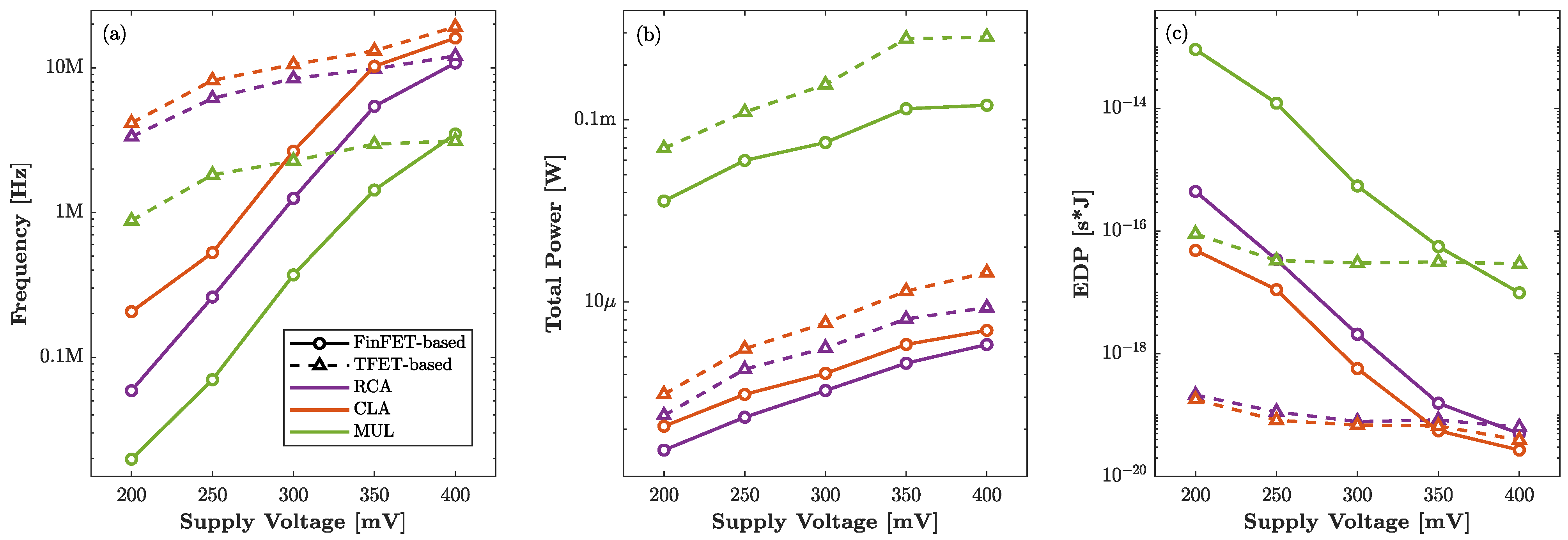
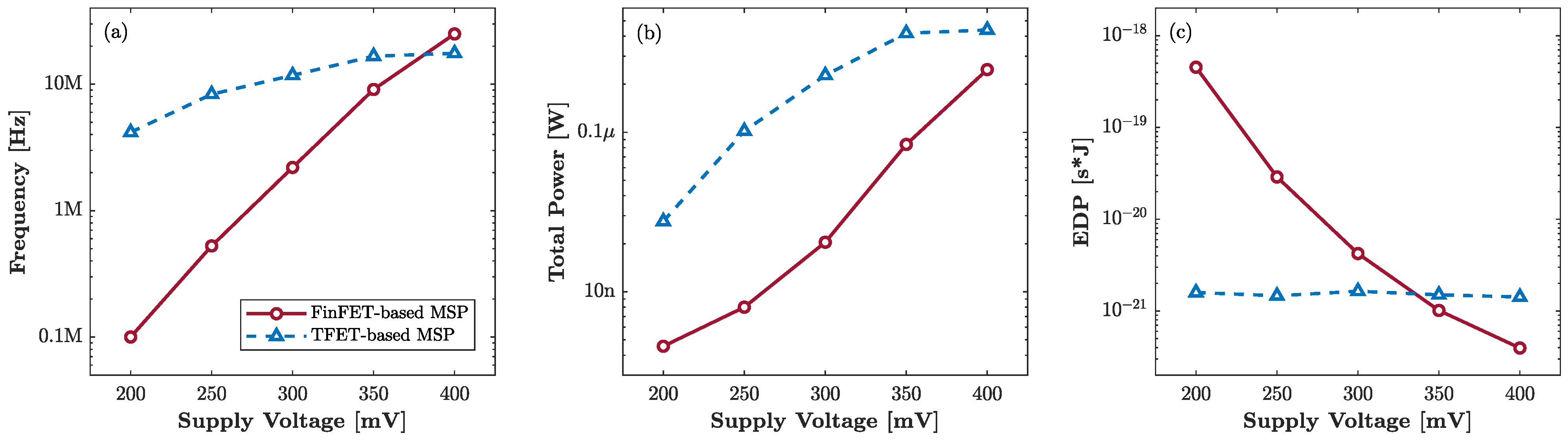
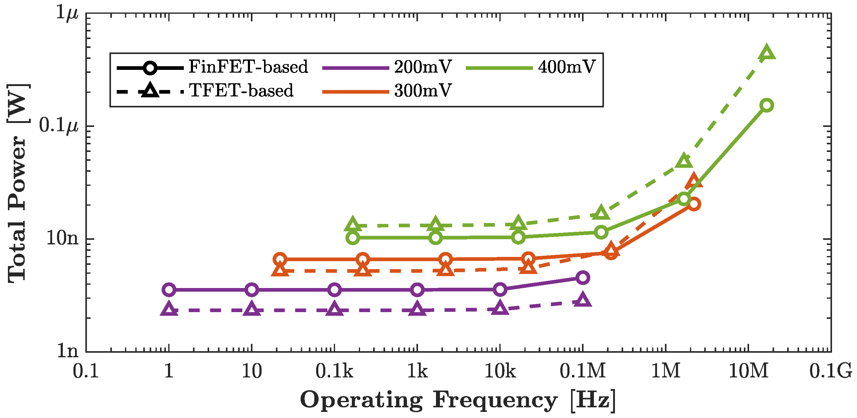
3.2. Synthesis Results

Now that the main characteristics of the primary logic gates (i.e., D Flip-Flop, Inverter, NAND2, and NOR2) of the standard cell libraries have been presented, the synthesis of more complex circuits is carried out in this section. Figure 8 presents the performance of three synthesized circuits based on TFET- and FinFET-based implementations: a 64-bit Ripple-Carry Adder (RCA), a 64-bit Carry Look-Ahead Adder (CLA), and a 32-bit multiplier (MUL) in terms of (a) maximum frequency of operation, (b) total power consumption, and (c) EDP. It is evident that the TFET-based implementations are better performing speed-wise since they are able to achieve higher frequencies of operation, being 14.1× faster (on average) than their FinFET-based counterparts. This tendency is more evident at lower supply voltages, around 250 mV. Moreover, the TFET-based circuits also consume more total power than the FinFET-based implementations, being on average 1.9× less power efficient. Nevertheless, when looking at the EDP figure-of-merit in Figure 8c, it is clear that the trade-off between energy consumption and performance is favorable to the TFET-based implementations at supply voltages below 375 mV.
The final standard benchmark is the synthesis of an MSP-430 (MSP) microcontroller [30]. The MSP synthesized in this work does not add any memory or peripherals to the simplest version of the microprocessor, and does not consider any optimization in terms of area, clock, or power. Although the developed standard cell libraries do not have area information of the characterized logic cells, the area can be estimated. TFET is modeled after a vertical nanowire and the FinFET as a conventional lateral transistor, estimating an area of 135 nm 2 and 145 nm 2 , respectively, [23]. This in turn allows us to extrapolate the total area that the combinational and sequential cells from the standard cell libraries can occupy on the MSP-430 synthesized design. While the gates in the FinFET-based MSP-430 synthesis occupy an estimated area of 7.37 μ m 2 , the TFET-based counterpart occupies 12.62 μ m 2 of area. It is evident that the sizing scheme causes the TFET implementation to occupy up to 71.2% more area.
The performance metrics of maximum frequency of operation, total power, and EDP are presented in Figure 9 to highlight the different behavior of TFET- and FinFET-based implementations. The TFET-based implementation can reach, on average, 13× higher frequencies than the FinFET-based MSP, with a staggering advantage of being 42× faster at an operating voltage of 200 mV. Still, the TFET-based implementation consumes an average of 6.7× more power across the ULV range. This value is higher than the average power consumption difference in the simple adder and multiplier modules, mainly because the MSP is not a purely combinational circuit. As shown in the EDP figure-of-merit of Figure 9c, the TFET-based MSP maintains a better (lower EDP) energy–speed trade-off at supply voltages below 340 mV. It is evident that while the TFET-based implementations require higher sizing ratios to diminish the inherent asymmetry of the device, they can provide a speed performance benefit much greater than the increased penalty in terms of power consumption when operating at ULVs.
Finally, the total power consumption behavior of TFET- and FinFET-based MSP synthesis at a fixed frequency of operation is shown in Figure 10 for the operating supply voltages of 200, 300, and 400 mV. The maximum operating frequency for both designs in this analysis at a given supply voltage is set by the slowest design between the TFET- and FinFET-based implementations, i.e., 17.5 MHz for TFET operating at 400 mV, and 0.1 MHz and 2.2 MHz for FinFET operating at 200 mV and 300 mV, respectively (since the TFET-based MSP is faster only at 200 mV and 300 mV). The TFET-based MSP operating at 400 mV always consumes a higher total power even at relaxed operating frequencies, being on average 71.2% more energy consuming than the FinFET-based implementation. At lower voltages, as compared with the FinFET-based MSP, the TFET-based solution achieves lower overall power consumption when the operating frequency is relaxed, being on average 3.3% and 34.8% more energy efficient at 300 mV and 200 mV, respectively. This analysis demonstrates that TFET-based implementations with relaxed speed performance requirements can compete with FinFET technologies while ensuring lower power consumption, especially in the ULV range.

4. Conclusions

This work presents a comparison in terms of speed and energy consumption of TFET- and FinFET-based circuits, including an MSP-430 benchmark intended for ultra-low-voltage operation. The main novelty of this work revolves around the use of TFET and FinFET transistors described through Look-Up Tables and Predictive Technology Models to create standard cell libraries by means of the Synopsys SiliconSmart tool. Overall, TFET-based circuits present lesser propagation delay, higher power consumption, smaller EDP, reduced leakage power, and higher input capacitance when compared with the FinFET-based implementations. These attributes were more prominent at ultra-low supply voltages. The synthesis of an MSP-430 benchmark demonstrates that, when compared with the FinFET-based MSP, the TFET-based solution was able to reach higher operating frequencies (with a maximum advantage of 41.6× at 200 mV) at the cost of higher power consumption (maximum penalty of 12.7× at 250 mV), which was proven to be a favorable trade-off due to a lower energy delay product. It was also shown that the MSP TFET-based implementations are able to present up to 1.62× less power consumption than their FinFET-based analogues at supply voltages as low as 200 mV when the frequency of operation is relaxed. The TFET device presents itself as an interesting alternative, able to reach better performance in terms of speed and energy efficiency at ultra-low supply voltages.

Author Contributions

Conceptualization, M.R., C.C., K.L., E.G., L.M.P. and R.T.; formal analysis, M.R., C.C., K.L., E.G., L.M.P. and R.T.; investigation, M.R., C.C., K.L., E.G., L.M.P. and R.T.; data curation, M.R., C.C., K.L., E.G., L.M.P. and R.T.; writing—original draft preparation, M.R., C.C., K.L., E.G., L.M.P. and R.T.; writing—review and editing, M.R., C.C., K.L., E.G., L.M.P. and R.T.; supervision, R.T. All authors have read and agreed to the published version of the manuscript.

Funding

This research received no external funding.

Institutional Review Board Statement

Not applicable.

Informed Consent Statement

Not applicable.

Data Availability Statement

The data that support the findings of this study are included within the article.

Conflicts of Interest

The authors declare no conflict of interest.

References

  1. Wang, A.; Chandrakasan, A. A 180 mV FFT processor using subthreshold circuit techniques. In Proceedings of the 2004 IEEE International Solid-State Circuits Conference (IEEE Cat. No.04CH37519), San Francisco, CA, USA, 15–19 February 2004; Volume 1, pp. 292–529. [Google Scholar] [CrossRef]
  2. Calhoun, B.; Chandrakasan, A. Characterizing and modeling minimum energy operation for subthreshold circuits. In Proceedings of the 2004 International Symposium on Low Power Electronics and Design (IEEE Cat. No.04TH8758), Newport Beach, CA, USA, 11 August 2004; pp. 90–95. [Google Scholar] [CrossRef]
  3. Zambrano, B.; Garzón, E.; Strangio, S.; Crupi, F.; Lanuzza, M. A 0.05 mm2, 350 mV, 14 nW Fully-Integrated Temperature Sensor in 180-nm CMOS. IEEE Trans. Circuits Syst. II Express Briefs 2021. [Google Scholar] [CrossRef]
  4. Lin, Z.; Li, L.; Wu, X.; Peng, C.; Lu, W.; Zhao, Q. Half-Select Disturb-Free 10T Tunnel FET SRAM Cell With Improved Noise Margin and Low Power Consumption. IEEE Trans. Circuits Syst. II Express Briefs 2021, 68, 2628–2632. [Google Scholar] [CrossRef]
  5. Frustaci, F.; Lanuzza, M.; Zicari, P.; Perri, S.; Corsonello, P. Designing high-speed adders in power-constrained environments. IEEE Trans. Circuits Syst. II Express Briefs 2009, 56, 172–176. [Google Scholar] [CrossRef]
  6. Alioto, M. Ultra-Low Power VLSI Circuit Design Demystified and Explained: A Tutorial. IEEE Trans. Circuits Syst. I Regul. Pap. 2012, 59, 3–29. [Google Scholar] [CrossRef]
  7. Taco, R.; Levi, I.; Lanuzza, M.; Fish, A. An 88-fJ/40-MHz [0.4 V]–0.61-pJ/1-GHz [0.9 V] Dual-Mode Logic 8 × 8 bit Multiplier Accumulator With a Self-Adjustment Mechanism in 28-nm FD-SOI. IEEE J.-Solid-State Circuits 2018, 54, 560–568. [Google Scholar] [CrossRef]
  8. Shavit, N.; Stanger, I.; Taco, R.; Lanuzza, M.; Fish, A. A 0.8-V, 1.54-pJ/940-MHz Dual-Mode Logic-Based 16 × 16-b Booth Multiplier in 16-nm FinFET. IEEE Solid-State Circuits Lett. 2020, 3, 314–317. [Google Scholar] [CrossRef]
  9. Vicuña, K.; Mosquera, C.; Musello, A.; Benedictis, S.; Rendón, M.; Garzón, E.; Prócel, L.M.; Trojman, L.; Taco, R. Energy Efficient Self-Adaptive Dual Mode Logic Address Decoder. Electronics 2021, 10, 1052. [Google Scholar] [CrossRef]
  10. Stanger, I.; Shavit, N.; Taco, R.; Lanuzza, M.; Fish, A. Silicon Evaluation of Multimode Dual Mode Logic for PVT-Aware Datapaths. IEEE Trans. Circuits Syst. II Express Briefs 2020, 67, 1639–1643. [Google Scholar] [CrossRef]
  11. Taco, R.; Levi, I.; Lanuzza, M.; Fish, A. Low voltage logic circuits exploiting gate level dynamic body biasing in 28 nm UTBB FD-SOI. Solid-State Electron. 2016, 117, 185–192. [Google Scholar] [CrossRef]
  12. Saripalli, V.; Datta, S.; Narayanan, V.; Kulkarni, J.P. Variation-tolerant ultra low-power heterojunction tunnel FET SRAM design. In Proceedings of the 2011 IEEE/ACM International Symposium on Nanoscale Architectures, San Diego, CA, USA, 8–9 June 2011; pp. 45–52. [Google Scholar] [CrossRef] [Green Version]
  13. Guo, L.; Ye, L.; Chen, C.; Huang, Q.; Yang, L.; Lv, Z.; An, X.; Huang, R. Benchmarking TFET from a circuit level perspective: Applications and guideline. In Proceedings of the 2017 IEEE International Symposium on Circuits and Systems (ISCAS), Baltimore, MD, USA, 28–31 May 2017; pp. 1–4. [Google Scholar] [CrossRef]
  14. Taco, R.; Levi, I.; Lanuzza, M.; Fish, A. Extended exploration of low granularity back biasing control in 28nm UTBB FD-SOI technology. In Proceedings of the 2016 IEEE International Symposium on Circuits and Systems (ISCAS), Montreal, QC, Canada, 22–25 May 2016; pp. 41–44. [Google Scholar] [CrossRef]
  15. Strangio, S.; Palestri, P.; Lanuzza, M.; Crupi, F.; Esseni, D.; Selmi, L. Assessment of InAs/AlGaSb Tunnel-FET Virtual Technology Platform for Low-Power Digital Circuits. IEEE Trans. Electron. Devices 2016, 63, 2749–2756. [Google Scholar] [CrossRef]
  16. Xie, Q.; Lin, X.; Wang, Y.; Chen, S.; Dousti, M.J.; Pedram, M. Performance Comparisons Between 7-nm FinFET and Conventional Bulk CMOS Standard Cell Libraries. IEEE Trans. Circuits Syst. II Express Briefs 2015, 62, 761–765. [Google Scholar] [CrossRef]
  17. Chen, S.; Wang, Y.; Lin, X.; Xie, Q.; Pedram, M. Performance prediction for multiple-threshold 7nm-FinFET-based circuits operating in multiple voltage regimes using a cross-layer simulation framework. In Proceedings of the 2014 SOI-3D-Subthreshold Microelectronics Technology Unified Conference (S3S), Millbrae, CA, USA, 6–9 October 2014; pp. 1–2. [Google Scholar] [CrossRef]
  18. Garzón, E.; Lanuzza, M.; Taco, R.; Strangio, S. Ultralow Voltage FinFET- Versus TFET-Based STT-MRAM Cells for IoT Applications. Electronics 2021, 10, 1756. [Google Scholar] [CrossRef]
  19. Zhang, Q.; Zhao, W.; Seabaugh, A. Low-subthreshold-swing tunnel transistors. IEEE Electron. Device Lett. 2006, 27, 297–300. [Google Scholar] [CrossRef]
  20. Arevalo, A.; Liautard, R.; Romero, D.; Trojman, L.; Procel, L.M. New Insight for next Generation SRAM: Tunnel FET versus FinFET for Different Topologies. In Proceedings of the 2019 32nd Symposium on Integrated Circuits and Systems Design (SBCCI), Sao Paulo, Brazil, 26–30 August 2019; pp. 1–6. [Google Scholar] [CrossRef]
  21. Strangio, S.; Palestri, P.; Lanuzza, M.; Esseni, D.; Crupi, F.; Selmi, L. Benchmarks of a III-V TFET technology platform against the 10-nm CMOS FinFET technology node considering basic arithmetic circuits. Solid-State Electron. 2017, 128, 37–42. [Google Scholar] [CrossRef]
  22. Heo, U.; Li, X.; Liu, H.; Gupta, S.; Datta, S.; Narayanan, V. A High-Efficiency Switched-Capacitance HTFET Charge Pump for Low-Input-Voltage Applications. In Proceedings of the 2015 28th International Conference on VLSI Design, Bangalore, India, 3–7 January 2015; pp. 304–309. [Google Scholar] [CrossRef]
  23. Strangio, S.; Settino, F.; Palestri, P.; Lanuzza, M.; Crupi, F.; Esseni, D.; Selmi, L. Digital and analog TFET circuits: Design and benchmark. Solid-State Electron. 2018, 146, 50–65. [Google Scholar] [CrossRef] [Green Version]
  24. Esseni, D.; Pala, M.G.; Rollo, T. Essential Physics of the OFF-State Current in Nanoscale MOSFETs and Tunnel FETs. IEEE Trans. Electron. Devices 2015, 62, 3084–3091. [Google Scholar] [CrossRef]
  25. Settino, F.; Lanuzza, M.; Strangio, S.; Crupi, F.; Palestri, P.; Esseni, D.; Selmi, L. Understanding the Potential and Limitations of Tunnel FETs for Low-Voltage Analog/Mixed-Signal Circuits. IEEE Trans. Electron. Devices 2017, 64, 2736–2743. [Google Scholar] [CrossRef]
  26. Wu, T.C.; Chen, C.J.; Chen, Y.N.; Hu, V.P.H.; Su, P.; Chuang, C.T. Evaluation of energy-efficient latch circuits with hybrid tunneling FET and FinFET devices for ultra-low-voltage applications. In Proceedings of the 2015 28th IEEE International System-on-Chip Conference (SOCC), Beijing, China, 8–11 September 2015; pp. 339–344. [Google Scholar] [CrossRef]
  27. Lanuzza, M.; Strangio, S.; Crupi, F.; Palestri, P.; Esseni, D. Mixed Tunnel-FET/MOSFET Level Shifters: A New Proposal to Extend the Tunnel-FET Application Domain. IEEE Trans. Electron. Devices 2015, 62, 3973–3979. [Google Scholar] [CrossRef] [Green Version]
  28. Morris, D.H.; Vaidyanathan, K.; Avci, U.E.; Liu, H.; Karnik, T.; Young, I.A. Enabling high-performance heterogeneous TFET/CMOS logic with novel circuits using TFET unidirectionality and low-VDD operation. In Proceedings of the 2016 IEEE Symposium on VLSI Technology, Honolulu, HI, USA, 14–16 June 2016; pp. 1–2. [Google Scholar] [CrossRef]
  29. ASU. Predictive Technology Model (PTM). Available online: http://ptm.asu.edu (accessed on 21 January 2021).
  30. Lin, L.; Jain, S.; Alioto, M. Sub-nW Microcontroller With Dual-Mode Logic and Self-Startup for Battery-Indifferent Sensor Nodes. IEEE J.-Solid-State Circuits 2021, 56, 1618–1629. [Google Scholar] [CrossRef]
Figure 1. Sketch of the device structure for n- and p-type (a) TFETs and (b) FinFET devices.
Electronics 11 00632 g001
Figure 2. Drain current of the (a) p-type and (b) n-type FinFET and TFET devices as a function of the gate-source voltage for drain-source voltage values of 0.1 V and 0.3 V. Drain current of the (c) p-type and (d) n-type FinFET and TFET devices as a function of the drain-source voltage for the gate-source voltage values of 0 to 0.4 V. Note that the calibration point is marked with an X. Gate capacitance of the (e) p-type and (f) n-type FinFET and TFET devices as a function of the gate-source voltage for drain-source voltage values of 0 V and 0.3 V.
Electronics 11 00632 g002
Figure 3. Butterfly plot at V D D = 300 mV for a (a) TFET-based and (b) FinFET-based inverter with W P / W N ratios of 3/1 and 1/1, respectively, showcasing the effect of the sizing methodology on the noise margin.
Electronics 11 00632 g003
Figure 4. Energy–delay plot over a supply voltage range from 300 mV to 500 mV for TFET and FinFET-based chains made out of inverters (INV), NAND2–NOR2, and NAND3–NOR3 gates.
Electronics 11 00632 g004
Figure 5. Energy–delay product over a supply voltage range from 300 mV to 500 mV for TFET and FinFET-based chains made out of inverters (INV), NAND2–NOR2, and NAND3–NOR3 gates.
Electronics 11 00632 g005
Figure 6. Leakage power over a wide supply voltage range for TFET and FinFET-based logic gates divided in (a) INV, NOR2, and NOR3 and (b) DFF, NAND2, and NAND3.
Electronics 11 00632 g006
Figure 7. Propagation delay for TFET and FinFET-based INV, and NOR2 at supply voltages of (a,b) 300 mV and (c,d) 400 mV over a wide range of input transition slope and load capacitance values.
Electronics 11 00632 g007
Figure 8. (a) Maximum frequency of operation, (b) total power consumption, and (c) EDP of a 64-bit Ripple-Carry Adder (RCA), a 64-bit Carry Look-Ahead Adder (CLA), and a 32-bit multiplier (MUL) based on TFET and FinFET devices across a supply voltage range of 200 mV to 400 mV.
Electronics 11 00632 g008
Figure 9. (a) Maximum frequency of operation, (b) total power consumption, and (c) EDP of a TFET- and FinFET-based MSP-430 across a supply voltage range of 200 mV to 400 mV.
Electronics 11 00632 g009
Figure 10. TFET- and FinFET-based MSP-430 total power consumption as a function of the operating frequency for the operating supply voltages of 200 mV, 300 mV, and 400 mV.
Electronics 11 00632 g010
Table 1. W P / W N ratios after the sizing process for an inverter (INV), NOR2, NOR3, NAND2, and NAND3 logic gates based on TFET and FinFET devices at V D D = 300 mV.
GateINVNOR2NOR3NAND2NAND3
TFET W P / W N 3/14/15/13/63/17
FinFET W P / W N 1/11/11/11/31/6
Table 2. Noise margin normalized to 50% of the supply voltage for FinFET and TFET-based INV, NOR2, NOR3, NAND2, NAND3 gates at 200, 300, and 400 mV.
V DD [mV]FinFET-BasedTFET-Based
INVNOR2NOR3NAND2NAND3INVNOR2NOR3NAND2NAND3
20070.8%69.2%67.7%72.3%72.5%66.0%65.0%65.0%68.0%69.0%
30077.6%77.6%77.5%80.5%80.9%74.0%75.5%75.0%77.4%78.1%
40081.2%81.2%81.2%84.5%84.0%67.0%62.3%60.0%65.4%66.7%
Table 3. Standard cell library specifications.
ParameterValue
Voltage (mV)200–500
Temperature (°C)25
ProcessTypical–Typical
Logic GatesDFF, INV, NAND2, NAND3*, NOR2, NOR3*
Technology10 nm
DevicesFinFET and TFET
Load Capacitance Range (fF)60–1000
Input Slope Range (ns)0.895–1288
Table 4. Input capacitance (fF).
GateFinFET-BasedTFET-Based
DFF-CLK267675
DFF-D94231
INV94231
NAND2189489
NAND33311060
NOR294290
NOR394350
Publisher’s Note: MDPI stays neutral with regard to jurisdictional claims in published maps and institutional affiliations.

