
From 32 nm to TFET Technology: New Perspectives for Ultra-Scaled RF-DC Multiplier Circuits


Abstract
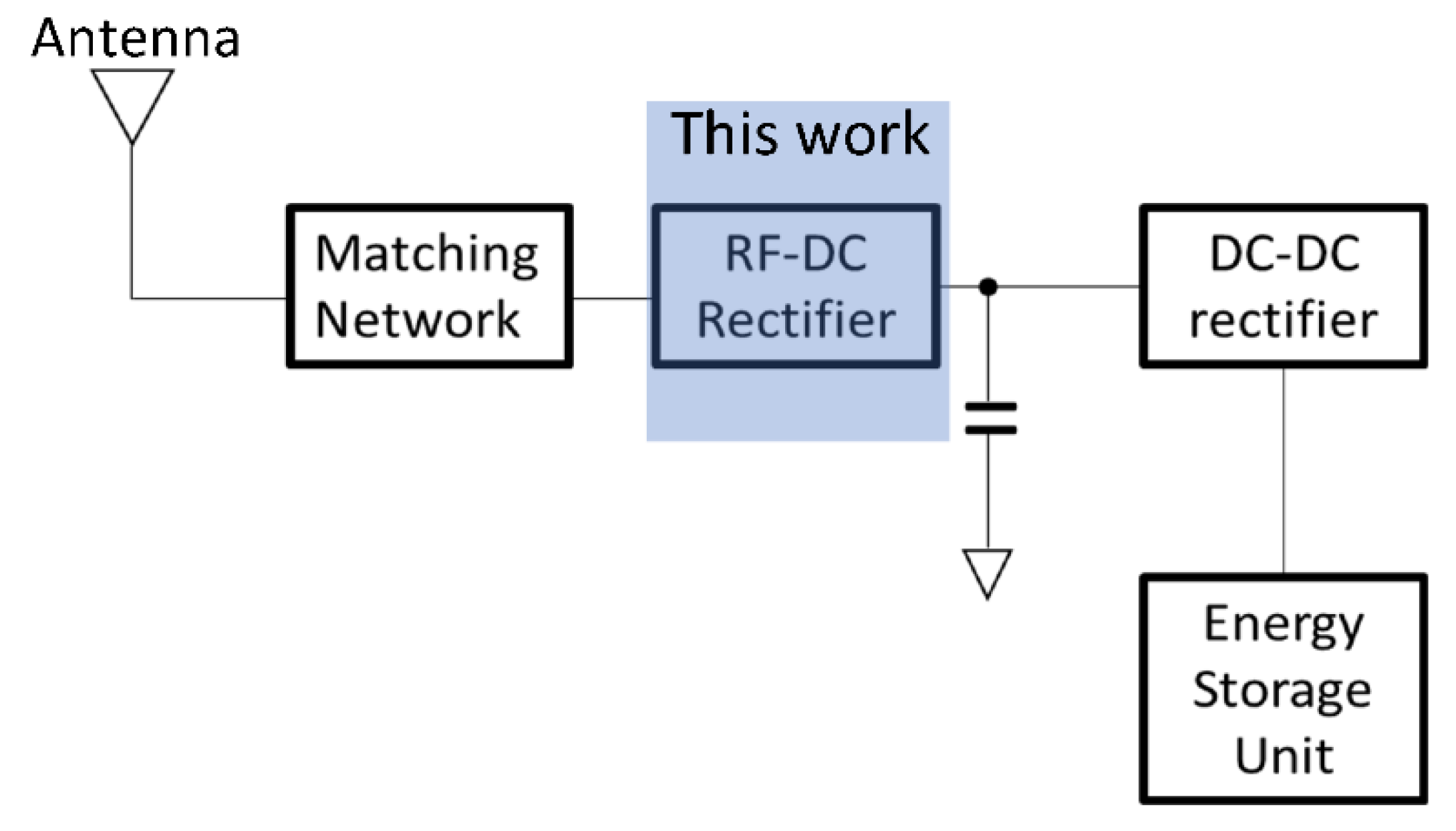
:1. Introduction
2. Technology and Topology
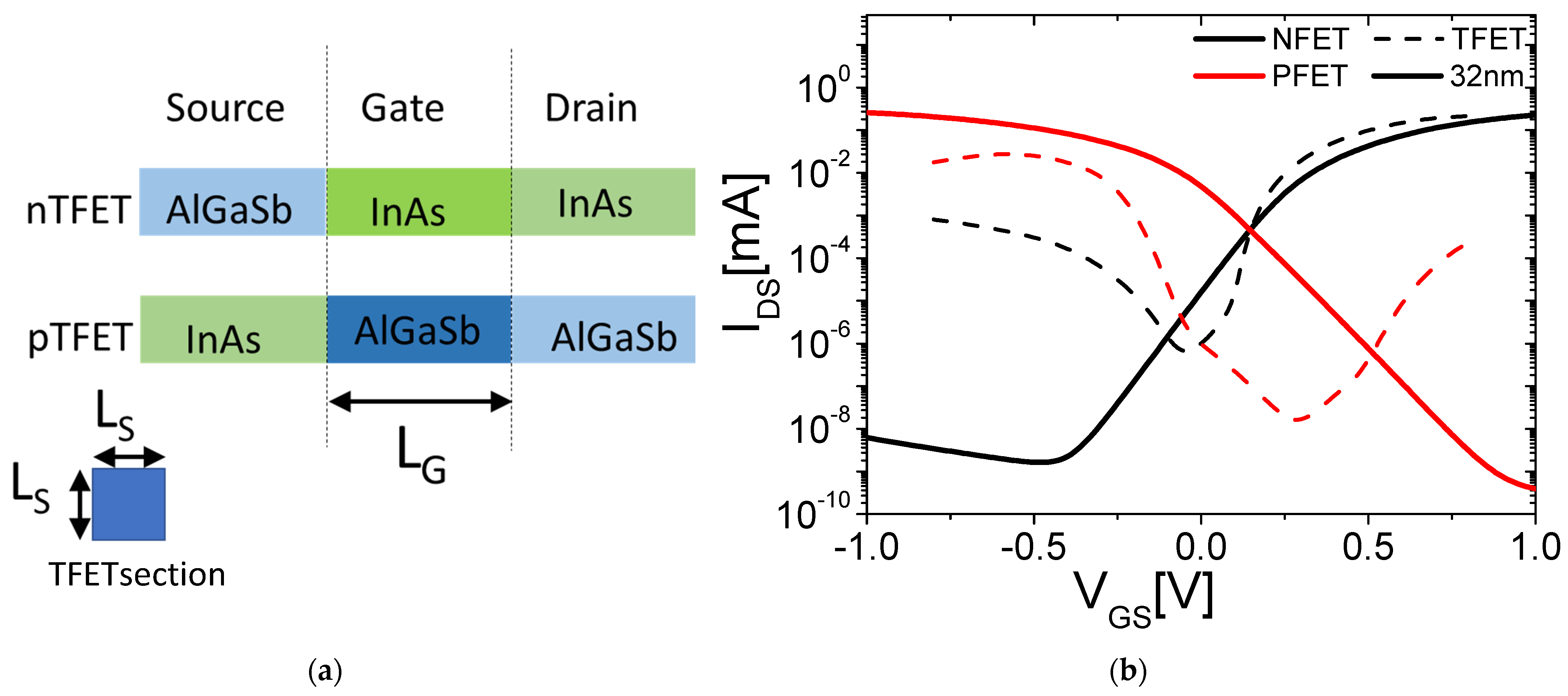
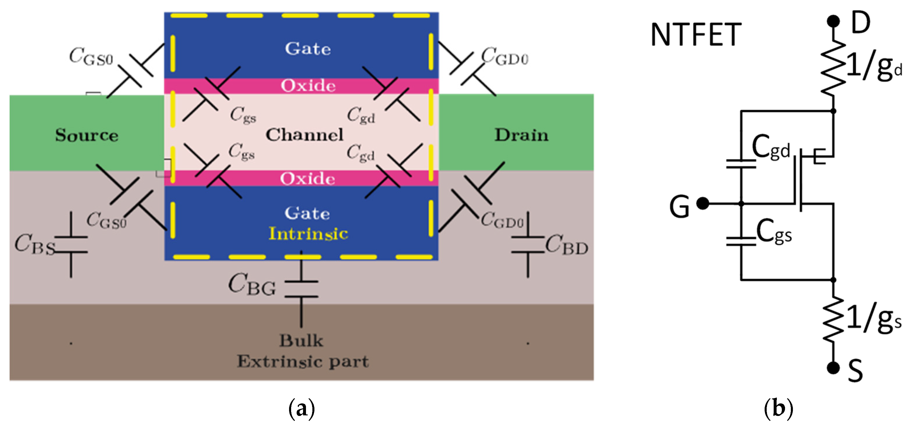
2.1. Technology
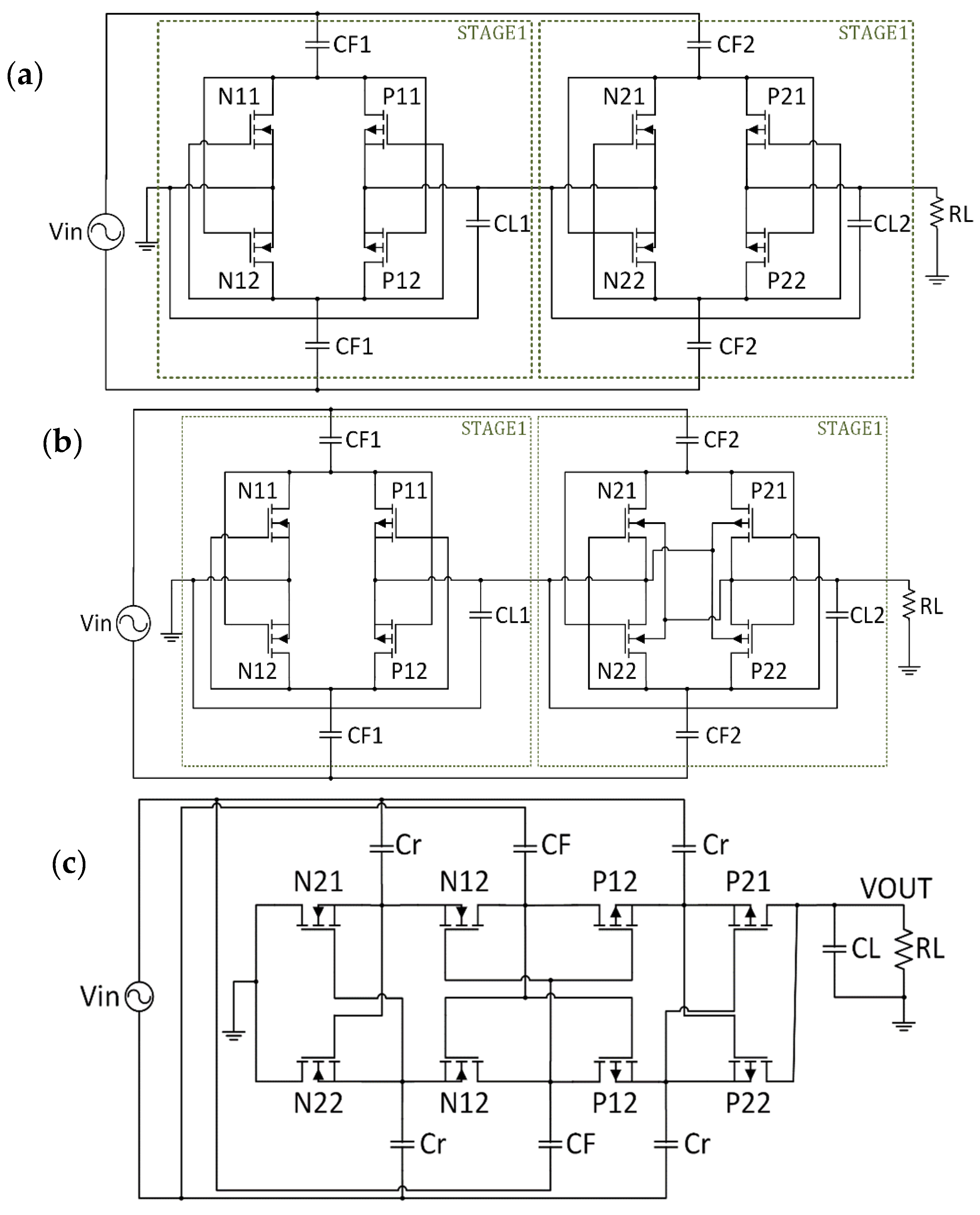
2.2. Topology
3. Design Optimization, Sizing, and Layout
3.1. Design Optimization and Sizing
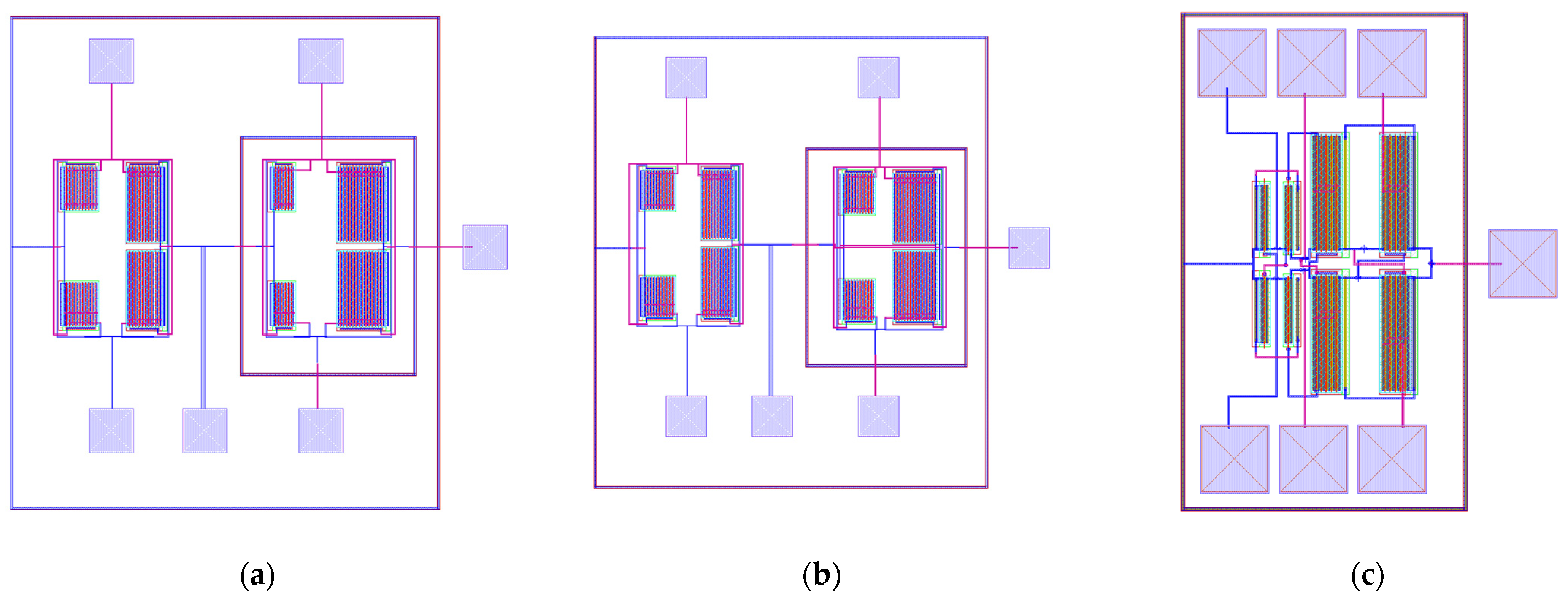
3.2. Layout and Parasitic Components
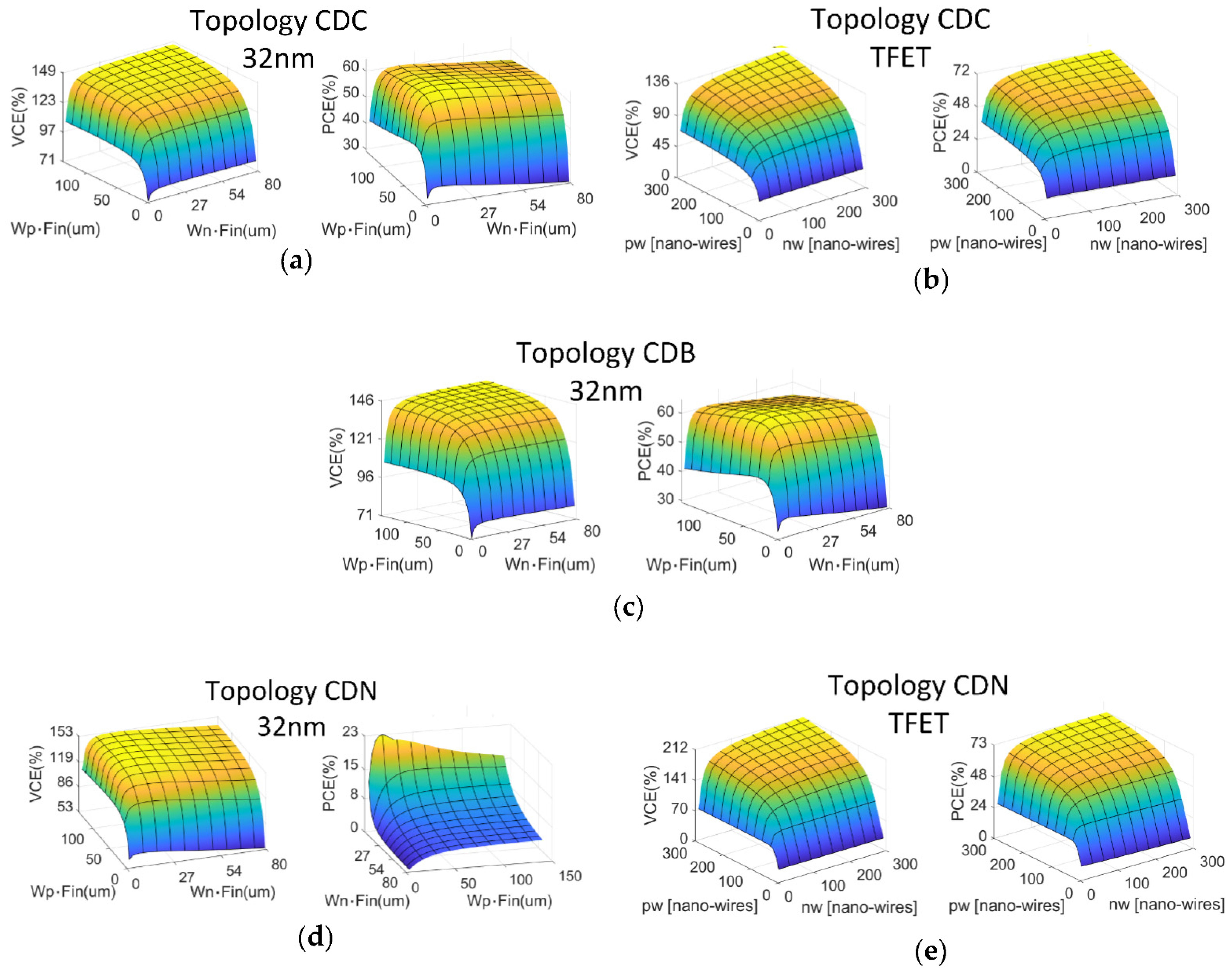
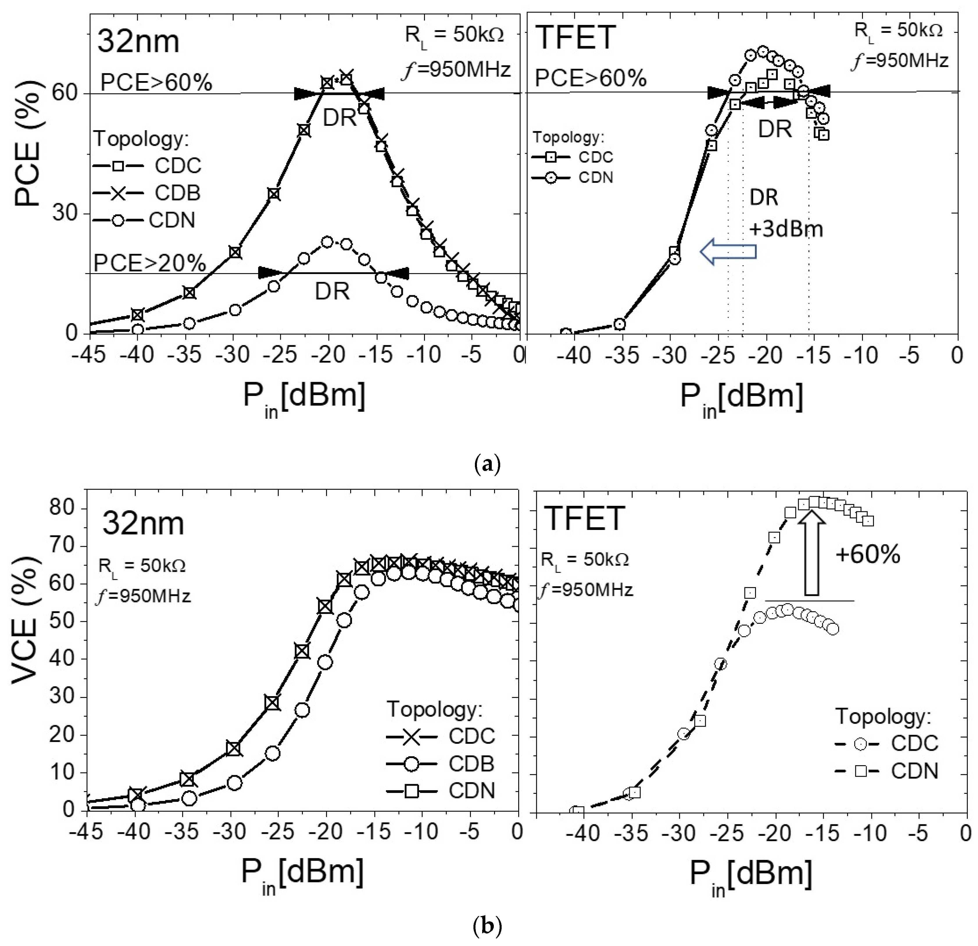
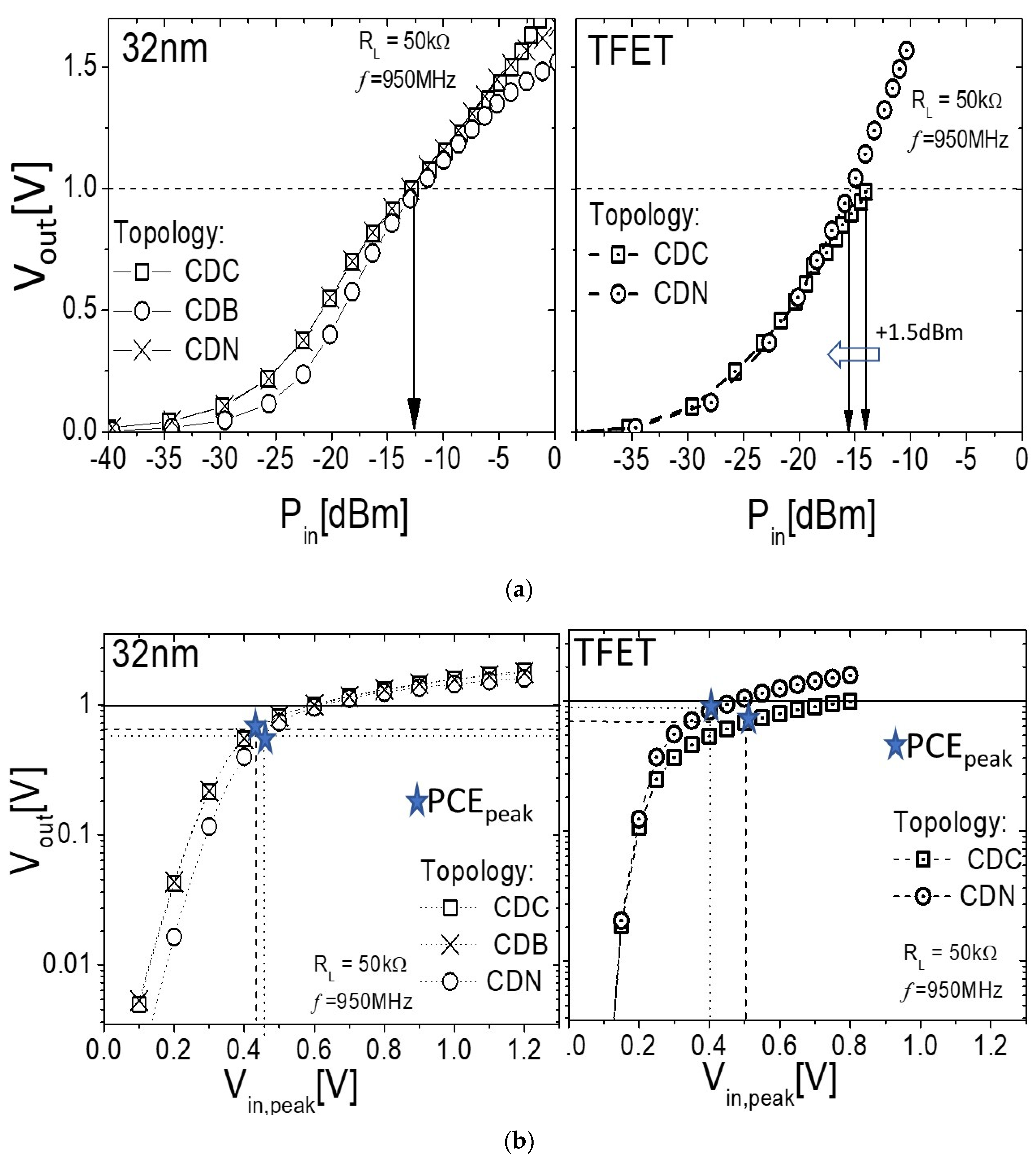
4. Results and Discussion
5. Conclusions
Author Contributions
Funding
Conflicts of Interest
References
- Clavelier, L.; Deguet, C.; Di Ciccio, L.; Augendre, E.; Brugere, A.; Guguen, P.; Le Tiec, Y.C.; Moreau, H.; Rabarot, M.; Signamarchaix, T.; et al. Engineered Substrates for Future More Moore and More than Moore integrated device. IEEE IEDM 2010, 2.6.1–2.6.4. [Google Scholar] [CrossRef]
- Poon, C.Y.; Lo, B.P.L.; Yuce, M.R.; Alomainy, A.; Hao, Y. Body sensor networks: In the era of big data and beyond. IEEE Rev. Biomed. Eng. 2015, 8, 4–16. [Google Scholar] [CrossRef]
- Hsieh, P.; Chou, C.; Chiang, T. An RF Energy Harvester With 44.1% PCE at Input Available Power of −12 dBm. IEEE Trans. Circuits Syst. I Regul. Pap. 2015, 62, 1528–1537. [Google Scholar] [CrossRef]
- Khan, D.; Abbasizadeh, H.; Kim, S.-Y.; Khan, Z.H.N.; Shah, S.A.A.; Pu, Y.G.; Hwang, K.C. A Design of Ambient RF Energy Harvester with Sensitivity of −21 dBm and Power Efficiency of a 39.3% Using Internal Threshold Voltage Compensation. Energies 2018, 11, 1158. [Google Scholar] [CrossRef] [Green Version]
- Wang, J.; Jiang, Y.; Dijkhuis, J.; Dolmans, G.; Gao, H.; Baltus, P. A 900MHz RFEH System in 40 nm CMOS Technology with Efficiency Peaking at 47% and Higher than 30% over 22 dB Wide input Power Range. In Proceedings of the 43rd IEEE European Solid State Circuits Conference (ESSCIRC), Leuven, Belgium, 11–14 September 2017. [Google Scholar]
- Ballo, A.; Bottaro, M.; Grasso, A.D. A review of power management integrated circuits for ultrasound-based energy harvesting in implantable medical devices. Electronics 2021, 11, 2487. [Google Scholar] [CrossRef]
- Sokrani, M.R.; Khodan, M.; Hamidon, M.N.B.; Kamsani, N.A.; Rokhani, F.Z.; Bin Shafle, S. An RF Energy Harvester System Using UHF Micropower CMOS Rectifier Based on a Diode Connected CMOS Transistor. Hindawi Sci. World J. 2014, 24, 963709. [Google Scholar]
- Kotani, K.; Sasaki, A.; Ito, T. High-Efficiency Differential-Drive CMOS Rectifier for UHF RFIDs. IEEE J. Solid-State Circuits 2009, 44, 3011–3018. [Google Scholar] [CrossRef]
- Ballo, A.; Bottaro, M.; Grasso, A.D. A review of charge pump topologies for the power management of IoT nodes. Electronics 2019, 8, 480. [Google Scholar] [CrossRef] [Green Version]
- Chong, G.; Ramiah, H.; Yin, J.; Rajendran, J.; Mak, P.; Martins, R.P. A Wide-PCE-Dynamic-Range CMOS Cross-Coupled Differential-Drive Rectifier for Ambient RF Energy Harvesting. IEEE Trans. Circuits Syst. II: Express Brief 2021, 68, 1743–1747. [Google Scholar] [CrossRef]
- Procel, L.-M.; Paredes, J.; Trojman, L. Comparison of Different Technologies for Transistor Rectifiers Circuits for Micropower Energy Harvesters. In Proceedings of the Latin American Electron Devices Conference (LAEDC), Armenia, Colombia, 24–27 February 2019; pp. 1–4. [Google Scholar]
- Rivadeneira, D.; Villegas, M.; Procel, L.M.; Trojman, L. Optimization of Active Voltage Rectifier/Doubler Designed in 90 nm Technology. In Proceedings of the IEEE LASCAS, San Jose, Costa Rica, 25–28 February 2020; pp. 1–4. [Google Scholar]
- Trojman, L.; Rivadeneira, D.; Villegas, M.; Acurio, E.; Lanuzza, M.; Procel, L.-M. RF-DC Multiplier for RF Energy Harvester based on 32 nm and TFET technologies. In Proceedings of the IEEE LASCAS, Arequipa, Peru, 21–24 February 2021; pp. 1–4. [Google Scholar]
- Gupta, N.; Makosiej, A.; Amara, A.; Vladimirescu, A.; Costin, A. State-of-the-Art TFET Devices. Chapter 2 of Book: TFET Integrated Circuits; Springer Link: Berlin/Heidelberg, Germany, 2020; pp. 5–15. [Google Scholar]
- Datta, S.; Liu, H.; Narayanan, V. Tunnel FET technology: A reliability perspective. Microelectron. Reliab. 2014, 54, 861–874. [Google Scholar] [CrossRef]
- Gupta, N.; Makosiej, N.; Amara, A.; Vladimirescu, A.; Costin, A. SRAMs, Chapter 3 of Book: TFET Integrated Circuits; Springer Link: Berlin/Heidelberg, Germany, 2020; pp. 17–43. [Google Scholar]
- Arevalo, A.; Liautard, R.; Romero, D.; Trojman, L.; Procel, L. New Insight for next Generation SRAM: Tunnel FET vs FinFET for Different Topologies. In Proceedings of the 32nd Symposium on Integrated Circuits and Systems Design (SBCCI), Sao Paulo, Brazil, 26–30 August 2019; pp. 1–6. [Google Scholar]
- Potocny, M.; Stopjakova, V.; Kovac, M. Self Vth-Compensating CMOS On-Chip Rectifier for Inductively Powered Implantable Medical Devices. In Proceedings of the 2018 IEEE 21st International Symposium on Design and Diagnostics of Electronic Circuits & Systems (DDECS), Budapest, Hungary, 25–27 April 2018. [Google Scholar]
- Chouhan, S.S.; Halonen, K. A 0.18 µm CMOS voltage multiplier arrangement for RF energy harvesting. Analog Integr. Circ. Sig. Process 2017, 92, 343–353. [Google Scholar]
- Strangio, S.; Settino, F.; Palestri, P.; Lanuzza, M.; Crupi, F.; Esseni, D.; Selmi, L. Digital and analog TFET circuits: Design and benchmark. Solid State Electron. 2018, 146, 50–65. [Google Scholar] [CrossRef] [Green Version]
- Baravelli, E.; Gnani, E.; Gnudi, A.; Reggiani, S.; Baccarani, G. TFET Inverters With n-/p-Devices on the Same Technology Platform for Low-Voltage/Low-Power Applications. IEEE Trans. Electron. Devices 2014, 61, 473–478. [Google Scholar] [CrossRef]
- Horst, F.; Farokhnejad, A.; Zhao, Q.-T.; Iniguez, B.; Loes, A. 2-D Physics-Based Compact DC Modeling of DG TFETs. IEEE Trans. Electron. Devices 2019, 66, 132–138. [Google Scholar] [CrossRef]
- Costin, A.; Gupta, H.A.; Amara, A.; Vladimirescu, A. 30-nm Tunnel FET with Improved Performance and reduced Ambipolar Current. IEEE Trans. Electron. Devices 2011, 58, 1649–1654. [Google Scholar]
- Luong, G.V.; Strangio, S.; Tiedmann, A.; Lenk, S.; Trellenkamp, S.; Bourdelle, K.K.; Zhao, Q.T.; Manti, S. Experimental demonstration of strained Si nanowire GAA n-TFETs and inverter operation with complementary TFET logic at low supply voltages. Solid-State Electron. 2016, 115, 152–159. [Google Scholar] [CrossRef]
- Saffarin, P.; Basaligheh, A.; Moez, K. An RF-to-DC Rectifier with High Efficiency over wide input power range for RF Energy Harvesting Applications. IEEE Trans. Circuits Syst. I Regul. Pap. 2019, 66, 4862–4875. [Google Scholar] [CrossRef]
- Xie, Z.; Wu, Z.; Wu, J. Technique Review for differential Drive Crossing Coupling Rectifier in RF Energy Harvester. Environment and Material Science (PEEMS). In Proceedings of the International Conference on Power, Energy, Dhaka, Bangladesh, 14–16 March 2019. [Google Scholar]
- Moghaddam, A.; Chuah, J.H.; Ramiah, H.; Ahmadia, J.; MaK, P.-I.; Martin, R.P. 73.9%-Efficiency CMOS Rectifier Using a LDCF Self-Body-Biasing Technique for Far-Field RF Energy-Harvesting Systems. IEEE Trans. Circ. Syst. I: Regul. Pap. 2017, 64, 992–1002. [Google Scholar] [CrossRef]
- Gao, H.; Matter-Kammerer, M.; Milosevic, D.; Linnartz, J.-P.; Baltus, P. A design of 2.4GHz rectifier in 65 nm CMOS with 31% efficiency. In Proceedings of the IEEE 20th Symposium on Communications and Vehicular Technology in the Benelux (SCVT), Namur, Belgium, 21 November 2013. [Google Scholar]
- Ouda, M.; Khalil, W.; Salama, K. Wide-Range Adaptive RF-to-DC Power Converter for UHF RFIDs. IEEE Microw. Wirel. Compon. Lett. 2016, 26, 634–636. [Google Scholar] [CrossRef]
- Haddad, P.-A.; Raskin, J.-P.; Flandre, D. Efficient passive energy harvesters at 950 MHz and 2.45 GHz for 100 μW applications in 65 nm CMOS. In Proceedings of the 23RD IEEE International Conference on Electronics, Circuits and Systems (ICECS), Monte Carlo, Monaco, 11–14 December 2016. [Google Scholar]
- Lanuzza, M.; Strangio, S.; Crupi, F.; Palestri, P.; Esseni, D. Mixed Tunnel-FET/MOSFET Level Shifters: A New Proposal to Extend the Tunnel-FET Application Domain. IEEE Trans. Electron Devices 2015, 6, 3973–3979. [Google Scholar] [CrossRef] [Green Version]
- Strangio, S.; Palestri, P.; Lanuzza, M.; Crupi, F.; Esseni, D.; Selmi, L. Assessment of InAs/AlGaSb Tunnel-FET Virtual Technology Platform for Low-Power Digital Circuits. IEEE Trans. Electron Devices 2016, 63, 2749–2756. [Google Scholar] [CrossRef]
- Settino, F.; Lanuzza, M.; Strangio, S.; Crupi, F.; Palestri, P.; Esseni, D.; Selmi, L. Understanding the Potential and Limitations of Tunnel FETs for Low-Voltage Analog/Mixed-Signal Circuits. IEEE Trans. Electron Devices 2017, 64, 2736–2743. [Google Scholar] [CrossRef]


| Circuit Sizing | CDC (TFET) | CDC (32 nm) | CDB (32 nm) | CDN (TFET) | CDN (32 nm) | |||
|---|---|---|---|---|---|---|---|---|
| Stage | 1 | 2 | 1 | 2 | 1 | 2 | 1 | 1 |
| CF [pF] | 10 | 20 | 10 | 10 | 10 | 10 | 10 | 1 |
| Cr [pF] | - | - | - | - | - | - | 5 | 1 |
| CL [pF] | 7 | 1 | 10 | 10 | 10 | 10 | 10 | 1 |
| RL [kΩ] | 50 | 50 | 50 | 50 | 50 | |||
| Total Wn [µm] | 40(300 NW) | 40(300 NW) | 2(10 Fin) | 2(6 Fin) | 2(10 Fin) | 2(10 Fin) | 2 | 2(1 Fin) |
| Total Wp [µm] | 40(300 NW) | 40(300 NW) | 3.5(10 Fin) | 3.5(14 Fin) | 3.5(14 Fin) | 3.5(14 Fin) | 3.5 | 3.5(10 Fin) |
| Length [nm] | 30 | 30 | 30 | 30 | 30 | |||
| CDC | CDB (Only 32 nm) | CDN | |||
|---|---|---|---|---|---|
| Techno | 32 nm | TFET | 32 nm | 32 nm | TFET |
| PCEpeak (%) | 64 | 64 | 64 | 23 | 70 |
| VCEpeak (%) | 65.5 | 53 | 65 | 63 | 82 |
| Vout@PCEpeak[V] | 0.65 | 0.7 | 0.65 | 0.6 | 0.9 |
| Pin@PCEpeak [dBm] | −18.5 | −19.5 | −18.5 | −19.4 | −20.2 |
| DR (>60%) [dBm] | 3.5 | 5 | 4 | N/A | 8 |
| Sensitivity@ 1 V [dBm] | −12.5 | −14 | −12.5 | −12.5 | −15.6 |
| Yield Factor (%) | 28 | 36 | 32 | - | 51 |
Publisher’s Note: MDPI stays neutral with regard to jurisdictional claims in published maps and institutional affiliations. |
© 2022 by the authors. Licensee MDPI, Basel, Switzerland. This article is an open access article distributed under the terms and conditions of the Creative Commons Attribution (CC BY) license (https://creativecommons.org/licenses/by/4.0/).
Share and Cite
Trojman, L.; Holguin, E.; Villegas, M.; Procel, L.-M.; Taco, R. From 32 nm to TFET Technology: New Perspectives for Ultra-Scaled RF-DC Multiplier Circuits. Electronics 2022, 11, 525. https://0-doi-org.brum.beds.ac.uk/10.3390/electronics11040525
Trojman L, Holguin E, Villegas M, Procel L-M, Taco R. From 32 nm to TFET Technology: New Perspectives for Ultra-Scaled RF-DC Multiplier Circuits. Electronics. 2022; 11(4):525. https://0-doi-org.brum.beds.ac.uk/10.3390/electronics11040525
Chicago/Turabian StyleTrojman, Lionel, Eduardo Holguin, Marco Villegas, Luis-Miguel Procel, and Ramiro Taco. 2022. "From 32 nm to TFET Technology: New Perspectives for Ultra-Scaled RF-DC Multiplier Circuits" Electronics 11, no. 4: 525. https://0-doi-org.brum.beds.ac.uk/10.3390/electronics11040525