
Temporary Bonding and Debonding in Advanced Packaging: Recent Progress and Applications
Abstract
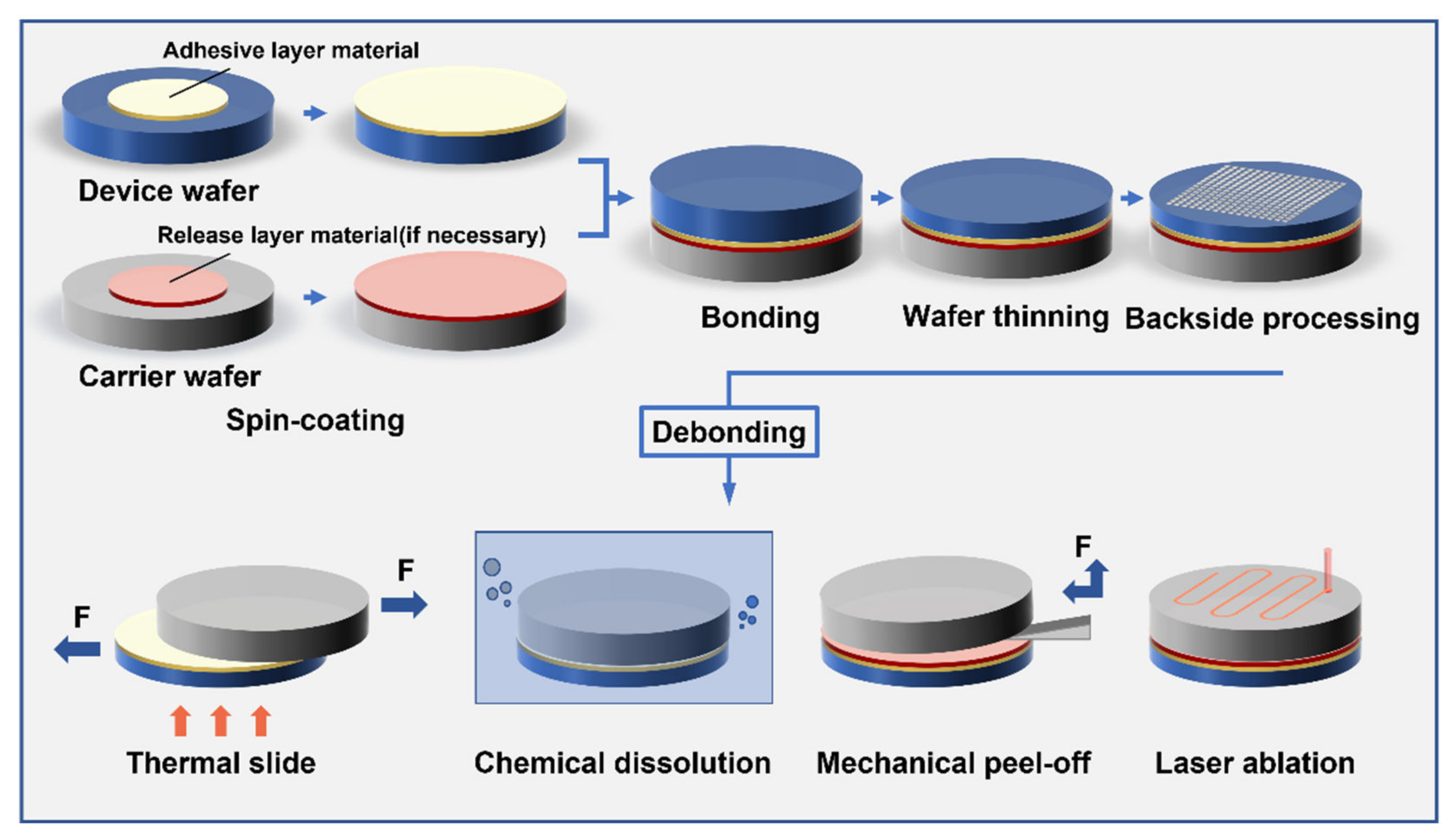
:1. Introduction
2. Advances in TBDB Technologies
2.1. Thermal Slide
2.2. Chemical Dissolution
2.3. Mechanical Peel-Off
2.4. Laser Ablation
2.5. Comparison
3. Applications in Advanced Packaging
3.1. Fan-Out Wafer Level Packaging
3.2. TSV and Cu-Cu Bonding
3.3. Two-Dimensional Material Transfer
4. Conclusions
Author Contributions
Funding
Data Availability Statement
Conflicts of Interest
References
- Wang, C.T.; Tang, T.C.; Lin, C.W.; Hsu, C.W.; Hsieh, J.S.; Tsai, C.H.; Wu, K.C.; Pu, H.P.; Yu, D. InFO_AiP Technology for High Performance and Compact 5G Millimeter Wave System Integration. In Proceedings of the 2018 IEEE 68th Electronic Components and Technology Conference (ECTC), San Diego, CA, USA, 29 May–1 June 2018; pp. 202–207. [Google Scholar]
- Nishimura, I.; Yamagami, M.; Oji, H.; Hayashi, T. Rdl-First Fowlp For Low-Density Applications With New Concept Fowlp Technology. In Proceedings of the 2020 International Wafer Level Packaging Conference (IWLPC), San Jose, CA, USA, 13–30 October 2020; pp. 1–6. [Google Scholar]
- Luo, R.; Wang, S.; Xia, Y.; Ma, S.; Wang, W.; Chen, J.; Jin, Y. Fabrication and Characterization of a Low Parasitic Capacitance and Low-Stress Si Interposer for 2.5-D Integration. IEEE Trans. Semicond. Manuf. 2018, 31, 521–527. [Google Scholar] [CrossRef]
- Lee, D.; Yoon, S.; Jun, J.; Park, J.; Lee, T.; Kang, U.B.; Lee, J. Improving flip chip process for large 2.5D molded interposer. In Proceedings of the 2021 IEEE 71st Electronic Components and Technology Conference (ECTC), San Diego, CA, USA, 1 June–4 July 2021; pp. 1026–1030. [Google Scholar]
- Rahim, M.K.; England, L.; Wang, Y.; Yu, D.; Wang, T. Simulation and Low Cost Process Development of Thin Wafer Level TSV Last Integration Scheme for RF Applications. In Proceedings of the 2018 19th International Conference on Electronic Packaging Technology (ICEPT), Shanghai, China, 8–11 August 2018; pp. 716–721. [Google Scholar]
- Wang, M.; Ma, S.; Cai, H.; Hu, L.; He, S. Design, Fabrication and Test of Dual Redundant TSV Interconnection for Millimeter Wave Applications. In Proceedings of the 2019 20th International Conference on Electronic Packaging Technology(ICEPT), Hong Kong, China, 12–15 August 2019; pp. 1–4. [Google Scholar]
- Marcinkevich, K.R.; Lunkov, P.V.; Kirienko, D.A.; Putrolaynen, V.V.; Belyaev, M.A.; Yartsev, A.V. Design, fabrication and testing of the package-on-package microcircuit. IOP Conf. Ser. Mater. Sci. Eng. 2021, 1155, 012096. [Google Scholar] [CrossRef]
- Pan, P.C.; Hsieh, T.L.; Huang, C.Y.; Jhong, M.F.; Wang, C.C. Design and electrical analysis for adavanced fan-out package-on-package. In Proceedings of the 2017 IEEE 19th Electronics Packaging Technology Conference (EPTC), Singapore, 6–9 December 2017; pp. 1–4. [Google Scholar]
- Su, J.; Niekiel, F.; Fichtner, S.; Thormaehlen, L.; Kirchhof, C.; Meyners, D.; Quandt, E.; Wagner, B.; Lofink, F. AlScN-based MEMS magnetoelectric sensor. Appl. Phys. Lett. 2020, 117, 132903. [Google Scholar] [CrossRef]
- Asri, M.I.A.; Hasan, M.N.; Fuaad, M.R.A.; Yunos, Y.M.; Ali, M.S.M. MEMS Gas Sensors: A Review. IEEE Sens. J. 2021, 21, 18381–18397. [Google Scholar] [CrossRef]
- Lin, S.L.; Huang, W.C.; Ko, C.T.; Chen, K.N. BCB-to-oxide bonding technology for 3D integration. Microelectron. Reliab. 2012, 52, 352–355. [Google Scholar] [CrossRef]
- Liu, J.; Liu, X.; Chen, B.; Feng, Z.; Qin, J.; Wu, M.; Chen, L.; Chen, X.; Liang, L. High-performance naphthalene epoxy resins cured by catalyst for packaging materials. Mater. Today Commun. 2022, 33, 104483. [Google Scholar] [CrossRef]
- Chen, L.-T.; Cheng, W.-H. Wafer-level chip scale packaging for piezoresistive pressure sensors using a dry-film shielding approach. Sens. Actuators A Phys. 2009, 152, 261–266. [Google Scholar] [CrossRef]
- Zhong, A.; Li, J.; Zhang, Y.; Zhang, F.; Wang, T.; Zhang, G.; Sun, R.; Wong, C.-P. Low temperature microwave fabrication of three-dimensional graphene/polyimide foams with flexibility strain responsivity. Compos. Part A-Appl. Sci. Manuf. 2020, 137, 105995. [Google Scholar] [CrossRef]
- Calvez, I.; Davoudi, S.; Szczepanski, C.R.; Landry, V. Low-gloss UV-curable coatings: Light mechanisms, formulations and processes—A review. Prog. Org. Coat. 2022, 171, 107039. [Google Scholar] [CrossRef]
- Ishida, H.; Lutter, S. Permanent Wafer Bonding and Temporary Wafer Bonding/De-Bonding Technology Using Temperature Resistant Polymers. J. Photopolym. Sci. Technol. 2014, 27, 173–176. [Google Scholar] [CrossRef] [Green Version]
- Huesgen, T.; Lenk, G.; Albrecht, B.; Vulto, P.; Lemke, T.; Woias, P. Optimization and characterization of wafer-level adhesive bonding with patterned dry-film photoresist for 3D MEMS integration. Sens. Actuat. A-Phys. 2010, 162, 137–144. [Google Scholar] [CrossRef]
- Shih, Y.-C.; Kim, G.; You, J.-P.; Shi, F.G. Printable optically transparent adhesive processing for bonding of LED chips to packages. Mater. Sci. Semicon. Proc. 2016, 56, 155–159. [Google Scholar] [CrossRef]
- Chen, G.; Ma, M.; Liu, Z.; Wei, A.; Zavabeti, A.; Hu, X.; Zhang, F.; Wang, B.; Mitchell, A.; Li, Y. Anodic bondable Li-Na-Al-B-Si-O glass-ceramics for Si—ULTCC heterogeneous integration. J. Eur. Ceram. Soc. 2019, 39, 2419–2426. [Google Scholar] [CrossRef]
- Landesberger, C.; Klink, G.; Schwinn, G.; Aschenbrenner, R. New dicing and thinning concept improves mechanical reliability of ultra thin silicon. In Proceedings of the Proceedings International Symposium on Advanced Packaging Materials Processes, Properties and Interfaces (IEEE Cat. No.01TH8562), Braselton, GA, USA, 11–14 March 2001; pp. 92–97. [Google Scholar]
- Puligadda, R.; Pilialamarri, S.; Hong, W.; Brubaker, C.; Wimplinger, M.; Pargfrieder, S. High-performance temporary adhesives for wafer bonding applications. Mater. Res. Soc. Symp. Proc. 2006, 970, 239–256. [Google Scholar] [CrossRef] [Green Version]
- Hashiguchi, H.; Fukushima, T.; Kino, H.; Lee, K.W.; Tanaka, T.; Koyanagi, M. A New Temporary Bonding Technology with Spin-on Glass and Hydrogenated Amorphous Si for 3D LSIs. In Proceedings of the 2014 International Conference on Electronics Packaging (ICEP), Toyama, Japan, 23–25 April 2014; pp. 74–77. [Google Scholar]
- Itabashi, T.; Zussman, M.P. High temperature resistant bonding solutions enabling thin wafer processing (Characterization of polyimide base temporary bonding adhesive for thinned wafer handling). In Proceedings of the 2010 Proceedings 60th Electronic Components and Technology Conference (ECTC), Las Vegas, NV, USA, 1–4 June 2010; pp. 1877–1880. [Google Scholar]
- Fritz, N.; Dao, H.; Allen, S.A.B.; Kohl, P.A. Polycarbonates as temporary adhesives. Int. J. Adhes. Adhes. 2012, 38, 45–49. [Google Scholar] [CrossRef]
- Rohwer, L.E.S.; Martin, J.E.; Friedmann, T.A.; Heck, J. Laser ablation of polyetheretherketone films for reversible wafer bonding. J. Laser Appl. 2012, 24, 022003. [Google Scholar] [CrossRef]
- Li, X.; Chen, P.; Qin, F.; Dong, X.; Xu, Q. Bionic PDMS-CDs surface with thermal controllable adhesion. Mater. Lett. 2020, 263, 127267. [Google Scholar] [CrossRef]
- Jouve, A.; Fowler, S.; Privett, M.; Puligadda, R.; Henry, D.; Astier, A.; Brun, J.; Zussy, M.; Sillon, N.; Burggraf, J.; et al. Facilitating Ultrathin Wafer Handling for TSV Processing. In Proceedings of the 2008 10th Electronics Packaging Technology Conference (EPTC), Singapore, 9–12 December 2008; pp. 45–50. [Google Scholar]
- Kettner, P.; Kim, B.; Pargfrieder, S.; Zhu, S. New Technologies for advanced high density 3D packaging by using TSV process. In Proceedings of the 2008 International Conference on Electronic Packaging Technology & High Density Packaging, Shanghai, China, 28–31 July 2008; pp. 43–45. [Google Scholar]
- Charbonnier, J.; Cheramy, S.; Henry, D.; Astier, A.; Brun, J.; Sillon, N.; Jouve, A.; Fowler, S.; Privett, M.; Puligadda, R.; et al. Integration of a Temporary Carrier in a TSV Process Flow. In Proceedings of the 2009 59th Electronic Components and Technology Conference (ECTC), San Diego, CA, USA, 26–29 May 2009; pp. 865–871. [Google Scholar]
- Pargfrieder, S.; Kettner, P.; Privett, M.; Ting, J. Temporary Bonding and DeBonding Enabling TSV Formation and 3D Integration for Ultra-thin Wafers. In Proceedings of the 2008 10th Electronics Packaging Technology Conference, Singapore, 9–12 December 2008; pp. 1301–1305. [Google Scholar]
- Pargfrieder, S.; Kim, B. Temporary bonding/debonding for ultrathin substrates. Solid State Technol. 2008, 51, 60–65. [Google Scholar]
- Mori, T.; Yamaguchi, T.; Maruyama, Y.; Hasegawa, K.; Kusumoto, S. Material Development for 3D Wafer Bond and De-bonding Process. In Proceedings of the Elec Comp C, San Diego, CA, USA, 26–29 May 2015; pp. 899–905. [Google Scholar]
- Tamura, K.; Nakada, K.; Taneichi, N.; Andry, P.; Knickerbocker, J.; Rosenthal, C. Novel Adhesive Development for CMOS-Compatible Thin Wafer Handling. In Proceedings of the 2010 Proceedings 60th Electronic Components and Technology Conference (ECTC), Las Vegas, NV, USA, 1–4 June 2010; pp. 1239–1244. [Google Scholar]
- Kubo, A.; Tamura, K.; Imai, H.; Yoshioka, T.; Oya, S.; Otaka, S. Development of New Concept Thermoplastic Temporary Adhesive for 3D-IC Integration. In Proceedings of the 2014 IEEE 64th Electronic Components and Technology Conference (ECTC), Orlando, FL, USA, 27–30 May 2014; pp. 899–905. [Google Scholar]
- Jourdain, A.; Phommahaxay, A.; Velenis, D.; Guerrero, A.; Bai, D.; Yess, K.; Arnold, K.; Miller, A.; Rebibis, K.; Beyer, G.; et al. Single-release-layer Process for Temporary Bonding Applications in the 3D Integration Area. In Proceedings of the Elec Comp C, San Diego, CA, USA, 26–29 May 2015; pp. 893–898. [Google Scholar]
- Webb, R. Temporary bonding enables new processes requiring ultra-thin wafers. Solid State Technol. 2010, 53, 10–12. [Google Scholar]
- Lee, A.; Su, J.; McCutcheon, J.; Wang, B.K.; Tsai, L.; Shorey, A. Optimization of Temporary Bonding through High-Resolution Metrologies to Realize Ultrathin Wafer Handling. In Proceedings of the 2012 IEEE 14th Electronics Packaging Technology Conference (EPTC), Singapore, 5–7 December 2012; pp. 322–325. [Google Scholar]
- Tsai, L.; Wang, B.K.; Shorey, A.; Lee, A.; Su, J.; Huang, B.; Shen, W.-W.; Chang, H.-H.; Chien, C.H. Laminating thin glass onto glass carrier to eliminate grinding and bonding process for glass interposer. In Proceedings of the 2014 IEEE 16th Electronics Packaging Technology Conference (EPTC), Singapore, 3–5 December 2014; pp. 545–548. [Google Scholar]
- Phommahaxay, A.; Potoms, G.; Verbinnen, G.; Sleeckx, E.; Beyer, G.; Beyne, E.; Guerrero, A.; Bai, D.; Liu, X.; Yess, K.; et al. Extremely Low-Force Debonding of Thinned CMOS Substrate by Laser Release of a Temporary Bonding Material. In Proceedings of the 2016 IEEE 66th Electronic Components and Technology Conference (ECTC), Las Vegas, NV, USA, 31 May–3 June 2016; pp. 1685–1690. [Google Scholar]
- Lee, A.; Su, J.; Huang, B.; Bai, D.; Shen, W.-W.; Chang, H.-H.; Chiang, C.-W. A Low-Temperature Temporary Lamination and Laser Debonding Technology to Enable Cost-Effective Fabrication of a Through-Glass-Via (TGV) Interposer on a Panel Substrate. In Proceedings of the 2015 IEEE 17th Electronics Packaging and Technology Conference (EPTC), Singapore, 2–4 December 2015; pp. 1–5. [Google Scholar]
- Tang, H.; Luo, C.; Yin, M.; Zeng, Y.; Zhang, W. High Throughput Air Jetting Wafer Debonding for 3D IC and MEMS Manufacturing. In Proceedings of the 2016 IEEE 66th Electronic Components and Technology Conference (ECTC), Las Vegas, NV, USA, 31 May–3 June 2016; pp. 1678–1684. [Google Scholar]
- Tang, H.; Shi, G.; He, R.; Yin, M.; Zhang, W.; Nguyen, M.; Chang, H.-H.; Yang, S.-S. High Throughput Low Stress Air Jetting Carrier Release for RDL-First Fan-Out Wafer-Level-Packaging. In Proceedings of the 2017 IEEE 67th Electronic Components and Technology Conference (ECTC), Orlando, FL, USA, 30 May–2 June 2017; pp. 1748–1754. [Google Scholar]
- Hashiguchi, H.; Fukushima, T.; Noriki, A.; Kino, H.; Lee, K.W.; Tanaka, T.; Koyanagi, M. Temporary Spin-on Glass Bonding Technologies for Via-Last/Backside-Via 3D Integration Using Multichip Self-Assembly. In Proceedings of the 2014 IEEE 64th Electronic Components and Technology Conference (ECTC), Orlando, FL, USA, 27–30 May 2014; pp. 856–861. [Google Scholar]
- Eichler, M.; Dillmann, H.; Reim, L.C.; Thomas, M.; Klages, C.P. Temporary Wafer Bonding by Polyelectrolyte Interlayers. ECS Trans. 2014, 64, 179–186. [Google Scholar] [CrossRef]
- Jeevendrakumar, V.J.B.; Pascual, D.N.; Bergkvist, M. Wafer Scale Solventless Adhesive Bonding with iCVD Polyglycidylmethacrylate: Effects of Bonding Parameters on Adhesion Energies. Adv. Mater. Interfaces 2015, 2, 1500076. [Google Scholar] [CrossRef]
- Matsumae, T.; Koehler, A.D.; Greenlee, J.D.; Anderson, T.J.; Baumgart, H.; Jernigan, G.G.; Hobart, K.D.; Kub, F.J. Temporary Bonding with Polydimethylglutarimide Based Lift Off Resist as a Layer Transfer Platform. ECS J. Solid State Sci. Technol. 2015, 4, 190–194. [Google Scholar] [CrossRef] [Green Version]
- Pargfrieder, S.; Burggraf, J.; Burgstaller, D.; Privett, M.; Jouve, A.; Henry, D.; Sillon, N. 3D integration with TSV: Temporary bonding and debonding. Solid State Technol. 2009, 52, 38–42. [Google Scholar]
- Kettner, P.; Burggraf, J.; Kim, B. Thin Wafer Handling and Processing- Results Achieved and Upcoming Tasks in the Field of 3D and TSV. In Proceedings of the 2009 11th Electronics Packaging Technology Conference, Singapore, 9–11 December 2009; pp. 787–789. [Google Scholar]
- Shuai, X.T.; Sun, R.; Zhang, G.P.; Deng, L.B. A Novel Temporary Adhesive for Thin Wafer Handling. In Proceedings of the 2014 15th International Conference on Electronic Packaging Technology (ICEPT), Chengdu, China, 12–15 August 2014; pp. 256–261. [Google Scholar]
- Deng, L.; Fang, H.; Shuai, X.; Zhang, G.; Wong, C.P.; Sun, R. Preparation of Reversible Thermosets and their Application in Temporary Adhesive for Thin Wafer Handling. In Proceedings of the Elec Comp C, San Diego, CA, USA, 26–29 May 2015; pp. 1197–1201. [Google Scholar]
- Phommahaxay, A.; Nakamura, A.; Jourdain, A.; Verbinnen, G.; Kamochi, Y.; Koyama, I.; Iwai, Y.; Sawano, M.; Tan, S.; Miller, A.; et al. Demonstration of a Novel Low Cost Single Material Temporary Bond Solution for High Topography Substrates based on a Mechanical Wafer Debonding and Innovative Adhesive Removal. In Proceedings of the Elec Comp C, San Diego, CA, USA, 26–29 May 2015; pp. 1430–1435. [Google Scholar]
- Zhu, Z.; Du, H.; Guan, Y.; Wang, H.; Yu, M.; Jin, Y.; Zhang, Z. Temporary Bonding/debonding Based on Propylene Carbonate. In Proceedings of the 2015 16th International Conference on Electronic Packaging Technology (ICEPT), Changsha, China, 11–14 August 2015; pp. 158–160. [Google Scholar]
- Zoschke, K.; Wegner, M.; Fischer, T.; Lang, K.-D. Temporary Handling Technology by Polyimide based Adhesive Bonding and Laser assisted De-bonding. In Proceedings of the 2016 6th Electronic System-Integration Technology Conference (ESTC), Grenoble, France, 13–15 September 2016; pp. 1–6. [Google Scholar]
- Cheng, C.-A.; Huang, Y.-H.; Lin, C.-H.; Lee, C.-L.; Yang, S.-C.; Chen, K.-N. Feasibility Investigation of Amorphous Silicon as Release Layer in Temporary Bonding for 3-D Integration and FOWLP Scheme. IEEE J. Electron. Devices Soc. 2017, 5, 136–140. [Google Scholar] [CrossRef]
- Hasegawa, K.; Mori, T.; Mizuno, H.; Ishii, H.; Maruyama, Y.; Ohkita, K. Laser releasable temporary bond/de-bond materials for next 3D packages. In Proceedings of the 2017 Pan Pacific Microelectronics Symposium (Pan Pacific), Kauai, HI, USA, 6–9 February 2017; pp. 1–7. [Google Scholar]
- Li, J.; Liu, Q.; Zhang, G.; Zhao, B.; Sun, R.; Wong, C.-P. Thermally Reversible and Crosslinked Polyurethane Based on Diels-Alder Chemistry for Ultrathin Wafer Temporary Bonding at Low-Temperature. In Proceedings of the 2017 IEEE 67th Electronic Components and Technology Conference (ECTC), Orlando, FL, USA, 30 May–2 June 2017; pp. 746–751. [Google Scholar]
- Xia, J.; Zhang, G. The effect of curing process on laser releasable de-bonding temporary material for 3D packages. In Proceedings of the 2017 18th International Conference on Electronic Packaging Technology (ICEPT), Harbin, China, 16–19 August 2017; pp. 1533–1536. [Google Scholar]
- Xue, X.; Yang, S.; Wang, Z. Heat-Depolymerizable Polypropylene Carbonate as a Temporary Bonding Adhesive for Fabrication of Flexible Silicon Sensor Chips. IEEE Trans. Compon. Packag. Manuf. Technol. 2017, 7, 1751–1758. [Google Scholar] [CrossRef]
- Zhu, Z.; Xu, Z. PPC-based bilayer temporary bonding and debonding. Microelectron. Eng. 2017, 180, 5–7. [Google Scholar] [CrossRef]
- Masuda, S.; Iwai, Y.; Sawano, M.; Okabe, K.; Shimada, K.; Caparas, J.A.; Choi, W.K. Temporary Bonding Material Study for Room Temperature Mechanical Debonding with eWLB Wafer Application. In Proceedings of the 2018 20th IEEE Electronics Packaging Technology Conference (EPTC), Singapore, 4–7 December 2018; pp. 500–503. [Google Scholar]
- Zhang, G.; Xia, J.; Liu, Q.; Huang, M.; Chen, W.; Sun, R.; Wong, C. Laser de-bonding solution for ultra-thin flexible device processing. J. Text. Res. 2018, 39, 155–159. [Google Scholar] [CrossRef]
- Zhang, H.; Liu, X.; Rickard, S.; Puligadda, R.; Flaim, T. Novel Temporary Adhesive Materials for RDL-First Fan-Out Wafer-Level Packaging. In Proceedings of the 2018 IEEE 68th Electronic Components and Technology Conference (ECTC), San Diego, CA, USA, 29 May–1 June 2018; pp. 1931–1936. [Google Scholar]
- Liu, X.; Bai, D.; Kirchner, L.; Puligadda, R.; Flaim, T. Advanced Multifunctional Temporary Bonding Materials with Heterogeneous Integrated Properties for Various Advanced Packaging Applications. In Proceedings of the 2019 China Semiconductor Technology International Conference (CSTIC), Shanghai, China, 18–19 March 2019; pp. 1–3. [Google Scholar]
- Yang, Y.S.; Hwang, K.S.; Gorrell, R. Laser Releasable Temporary Bonding Film with High Thermal Stability. In Proceedings of the 2019 IEEE 69th Electronic Components and Technology Conference (ECTC), Las Vegas, NV, USA, 28–31 May 2019; pp. 330–333. [Google Scholar]
- Zigmond, J.; Gray, A.; Moore, J. Chemical and Temperature Resistance of PIB-Based Temporary Adhesives. In Proceedings of the IEEE 21st Electronics Packaging Technology Conference (EPTC), Singapore, 4–6 December 2019; pp. 217–223. [Google Scholar]
- Araki, N.; Maetani, S.; Kim, Y.; Hirota, T.; Nakamura, T.; Ohba, T. Material Optimization of Permanent and Temporary Adhesives for Wafer-level Three-dimensional Integration. In Proceedings of the 2020 IEEE 70th Electronic Components and Technology Conference (ECTC), Orlando, FL, USA, 3–30 June 2020; pp. 56–61. [Google Scholar]
- Liu, X.; Kirchner, L.; Prenger, L.; Cheng, W.; Puligadda, R. A Single-Layer Solution with Laser Debonding Technology for Temporary Bond/Debonding Applications in Wafer-Level Packaging. In Proceedings of the 2020 China Semiconductor Technology International Conference (CSTIC), Shanghai, China, 26 June–17 July 2020; pp. 1–4. [Google Scholar]
- Shiojima, T.; Watanabe, R.; Hatai, M.; Sugita, D. Development of Self-releasing adhesive tape as a temporary bonding material for 3D integration. In Proceedings of the 2020 IEEE 70th Electronic Components and Technology Conference (ECTC), Orlando, FL, USA, 3–30 June 2020; pp. 75–82. [Google Scholar]
- Xu, D.; Wang, H.-W.; Patel, J.; Brun, X.F.; Hirota, K.; Capsuto, E.; Kato, H.; Sugo, M. A Novel Design of Temporary Bond Debond Adhesive Technology for Wafer-Level Assembly. In Proceedings of the 2020 IEEE 70th Electronic Components and Technology Conference (ECTC), Orlando, FL, USA, 3–30 June 2020; pp. 68–74. [Google Scholar]
- Hwang, K.; Kim, K.-S.; Gorrell, R.; Kim, K.-w.; Yang, Y.-s.; Zou, W. Laser Releasable Temporary Bonding Film for Fanout Process with Large Panel. In Proceedings of the 2021 IEEE 71st Electronic Components and Technology Conference (ECTC), San Diego, CA, USA, 1 June–4 July 2021; pp. 754–761. [Google Scholar]
- Liu, X.; Wang, Y.; Blumenshine, D.; Dong, M.; Puligadda, R. A Single-Layer Mechanical Debonding Adhesive for Advanced Wafer-Level Packaging. In Proceedings of the 2021 IEEE 71st Electronic Components and Technology Conference (ECTC), San Diego, CA, USA, 1 June–4 July 2021; pp. 711–716. [Google Scholar]
- Ye, Z.; Sun, D.; Huang, M.; Zhang, G.; Xia, J. An Infrared Laser Temporary Bonding Material Used for Device Wafer Thinning and Completion of Backside Processing Technology. In Proceedings of the 2021 22nd International Conference on Electronic Packaging Technology (ICEPT), Xiamen, China, 14–17 September 2021; pp. 1–4. [Google Scholar]
- Montmeat, P.; Le Cocq, M.; Enot, T.; Zussy, M.; Fournel, F. Impact of the temperature process on the morphology of 3D temporary bonded wafers: Quantification and reducing of the effect. Mater. Sci. Semicon. Proc. 2021, 136, 106156. [Google Scholar] [CrossRef]
- Zussman, M.P.; Milasincic, C.; Rardin, A.; Kirk, S.; Itabashi, T. Using Permanent and Temporary Polyimide Adhesives in 3D-TSV Processing to Avoid Thin Wafer Handling. J. Microelectron. Electron. Packag. 2010, 7, 214–219. [Google Scholar] [CrossRef]
- Phommahaxay, A.; Jourdain, A.; Potoms, G.; Verbinnen, G.; Sleeckx, E.; Beyer, G.; Beyne, E.; Guerrero, A.; Bai, D.; Yess, K.; et al. Advances in Thin Wafer Debonding and Ultrathin 28-nm FinFET Substrate Transfer. In Proceedings of the 2017 IEEE 67th Electronic Components and Technology Conference (ECTC), Orlando, FL, USA, 30 May–2 June 2017; pp. 740–745. [Google Scholar]
- Fowler, M.; Massey, J.P.; Trichur, R.K.; Koch, M. Dual-Carrier Process Using Mechanical and Laser Release Technologies for Advanced Wafer-Level Packaging. In Proceedings of the 2018 IEEE 68th Electronic Components and Technology Conference (ECTC), San Diego, CA, USA, 29 May–1 June 2018; pp. 1214–1219. [Google Scholar]
- Wuensch, D.; Purwin, L.; Buettner, L.; Martinka, R.; Schubert, I.; Junghans, R.; Baum, M.; Wiemer, M.; Otto, T. Temporary wafer bonding—Key technology for MEMS devices. In Proceedings of the 2017 Pan Pacific Microelectronics Symposium (Pan Pacific), Kauai, HI, USA, 6–9 February 2017; pp. 1–7. [Google Scholar]
- Podpod, A.; Phommahaxay, A.; Bex, P.; Kennes, K.; Bertheau, J.; Arumugam, H.; Cochet, T.; Rebibis, K.; Sleeckx, E.; Miller, A.; et al. Novel Temporary Bonding and Debonding Solutions Enabling an Ultrahigh Interonnect Density Fo-Wlp Structure Assembly with Quasi-Zero Die Shift. In Proceedings of the 2019 International Wafer Level Packaging Conference (IWLPC), San Jose, CA, USA, 22–24 October 2019; pp. 1–6. [Google Scholar]
- Phommahaxay, A.; Potoms, G.; Bertheau, J.; Bex, P.; Duval, F.; Podpod, A.; Wang, T.; Verbinnen, G.; Beyer, G.; Sleeckx, E.; et al. A Unique Temporary Bond Solution Based on a Polymeric Material Tacky at Room Temperature and Highly Thermally Resistant Application Extension from 3D-SIC to FO-WLP. In Proceedings of the 2017 IEEE 67th Electronic Components and Technology Conference (ECTC), Orlando, FL, USA, 30 May–2 June 2017; pp. 1829–1834. [Google Scholar]
- Sekhar, V.N.; Ji, H.; Arimoto, S.; Okazawa, T.; Fujiwara, T.; Kawano, M. Evaluation of Single Layer Adhesive Material for Thin Wafer Handling Applications. In Proceedings of the 2017 IEEE 19th Electronics Packaging Technology Conference (EPTC), Singapore, 6–9 December 2017; pp. 1–4. [Google Scholar]
- Bertheau, J.; Inoue, F.; Phommahaxay, A.; Peng, l.; Iacovo, S.; Rassoul, N.; Sleeckx, E.; Rebibs, K.; Miller, A.; Beyer, G.; et al. Extreme Thinned-Wafer Bonding Using Low Temperature Curable Polyimide for Advanced Wafer Level Integrations. In Proceedings of the 2018 IEEE 68th Electronic Components and Technology Conference (ECTC), San Diego, CA, USA, 29 May–1 June 2018; pp. 86–91. [Google Scholar]
- Li, K.; Bai, Y.; Liu, Q.; Li, J.; Li, Z.; Dai, W.; Wang, X.; Zhang, G. A Novel High Temperature Resistant Temporary Bonding Material for Ultra-thin Wafer Handling: Superior Room Temperature Bonding, Heat Curing and Mechanical De-bonding Performances. In Proceedings of the 2022 23rd International Conference on Electronic Packaging Technology (ICEPT), Dalian, China, 10–13 August 2022; pp. 1–4. [Google Scholar]
- Kim, Y.; Park, S.; Kim, B.-K.; Park, W.-J.; Kim, H.J. Laser lift-off of polyimide thin-film from glass carrier using DPSS laser pulses of top-hat square profiles. Opt. Laser. Technol. 2021, 142, 107245. [Google Scholar] [CrossRef]
- Montmeat, P.; Enot, T.; Dutra, M.D.M.; Pellat, M.; Fournel, F. Study of a silicon/glass bonded structure with a UV-curable adhesive for temporary bonding applications. Microelectron. Eng. 2017, 173, 13–21. [Google Scholar] [CrossRef]
- Kennes, K.; Phommahaxay, A.; Guerrero, A.; Bumueller, D.; Suhard, S.; Bex, P.; Tussing, S.; Liu, X.; Beyer, G.; Beyne, E. Acoustic modulation during laser debonding of collective hybrid bonded dies. In Proceedings of the 2021 IEEE 71st Electronic Components and Technology Conference (ECTC), San Diego, CA, USA, 1 June–4 July 2021; pp. 2126–2133. [Google Scholar]
- Kennes, K.; Phommahaxay, A.; Guerrero, A.; Suhard, S.; Bex, P.; Brems, S.; Liu, X.; Tussing, S.; Beyer, G.; Beyne, E. Carrier Systems for Collective Die-to-Wafer Bonding. In Proceedings of the 2022 IEEE 72nd Electronic Components and Technology Conference (ECTC), San Diego, CA, USA, 31 May–3 June 2022; pp. 2058–2063. [Google Scholar]
- Wang, F.; Liu, Q.; Wang, X.; Li, J.; Zhang, G.; Sun, R. Nondestructive Laser Debonding of Designable Responsive and Buffer Layers for Wafer Level Packaging. In Proceedings of the 2022 23rd International Conference on Electronic Packaging Technology (ICEPT), Dalian, China, 10–13 August 2022; pp. 1–4. [Google Scholar]
- Bai, D.; Liu, X.; Zhang, H.; Wu, Q.; Trichur, R.; Puligadda, R.; Flaim, T. Laser release technology for wafer level packaging. In Proceedings of the 2018 China Semiconductor Technology International Conference (CSTIC), Shanghai, China, 11–12 March 2018; pp. 1–3. [Google Scholar]
- Dai, W.; Liu, Q.; Li, Z.; Li, K.; Wang, X.; Wang, F.; Li, J.; Sun, R.; Zhang, G. A Novel Single-Layer High-Temperature-Resistant Adhesive Layer Applied in Advanced Wafer-Level Packaging. In Proceedings of the 2022 23rd International Conference on Electronic Packaging Technology (ICEPT), Dalian, China, 10–13 August 2022; pp. 1–4. [Google Scholar]
- Daido, I.; Watanabe, R.; Takahashi, T.; Hatai, M. Development of a Temporary Bonding Tape Having over 300 degC Thermal Resistance for Cu-Cu Direct Bonding. In Proceedings of the 2021 IEEE 71st Electronic Components and Technology Conference (ECTC), San Diego, CA, USA, 1 June–4 July 2021; pp. 693–699. [Google Scholar]
- Wang, X.; Liu, Q.; Wang, F.; Li, J.; Li, Z.; Dai, W.; Huang, M.; Li, K.; Bai, Y.; Zhang, G.; et al. Temporary bonding system with photopolymer release layer for 365nm UV debonding without laser. In Proceedings of the 2022 23rd International Conference on Electronic Packaging Technology (ICEPT), Dalian, China, 10–13 August 2022; pp. 1–5. [Google Scholar]
- Tseng, C.F.; Liu, C.S.; Wu, C.H.; Yu, D. InFO (Wafer Level Integrated Fan-Out) Technology. In Proceedings of the 2016 IEEE 66th Electronic Components and Technology Conference (ECTC), Las Vegas, NV, USA, 31 May–3 June 2016; pp. 1–6. [Google Scholar]
- Ji, Y.; Wang, C.; Li, Y. Development, Challenges and Opportunities of Fan-out Packaging. Electron. Packag. 2020, 20, 080101. [Google Scholar] [CrossRef]
- Wu, Q.; Liu, X.; Han, K.; Bai, D.; Flaim, T. Temporary Bonding and Debonding Technologies for Fan-Out Wafer-Level Packaging. In Proceedings of the 2017 IEEE 67th Electronic Components and Technology Conference (ECTC), Orlando, FL, USA, 30 May–2 June 2017; pp. 890–895. [Google Scholar]
- Podpod, A.; Phommahaxay, A.; Bex, P.; Slabbekoorn, J.; Bertheau, J.; Salahoueldhadj, A.; Sleeckx, E.; Miller, A.; Beyer, G.; Beyne, E.; et al. Advances in Temporary Carrier Technology for High-Density Fan-Out Device Build-up. In Proceedings of the 2019 IEEE 69th Electronic Components and Technology Conference (ECTC), Las Vegas, NV, USA, 28–31 May 2019; pp. 340–345. [Google Scholar]
- Phommahaxay, A.; Podpod, A.; Slabbekoorn, J.; Sleeckx, E.; Beyer, G.; Beyne, E.; Guerrero, A.; Bai, D.; Arnold, K. Advances in Temporary Bonding and Release Technology for Ultrathin Substrate Processing and High-Density Fan-Out Device Build-up. In Proceedings of the 2018 IEEE 68th Electronic Components and Technology Conference (ECTC), San Diego, CA, USA, 29 May–1 June 2018; pp. 985–992. [Google Scholar]
- Thermal Slide Debonding For Temporary Bonding Processes (Part 3 Of 3). Available online: https://cn.brewerscience.com/bid-95825-thermal-slide-debonding-for-temporary-bonding-processes-part-3-of-3/# (accessed on 14 March 2023).
- Tyler, P.; Nulman, K.; Mauer, L.; Fowler, M.; Molenhour, S. Temporary Bonding and the Challenge of Cleaning Post-Debond. In Proceedings of the 2018 International Wafer Level Packaging Conference (IWLPC), San Jose, CA, USA, 23–25 October 2018; pp. 1–7. [Google Scholar]
- Medina, H.; Lin, Y.-C.; Jin, C.; Lu, C.-C.; Yeh, C.-H.; Huang, K.-P.; Suenaga, K.; Robertson, J.; Chiu, P.-W. Metal-Free Growth of Nanographene on Silicon Oxides for Transparent Conducting Applications. Adv. Funct. Mater. 2012, 22, 2123–2128. [Google Scholar] [CrossRef]
- Qian, Y.; Sohn, M.K.; Park, H.J.; Hwang, J.S.; Subramanian, K.R.V.; Kang, D.J. Universal 2D material film transfer using a novel low molecular weight polyvinyl acetate. Appl. Surf. Sci. 2020, 534, 147650. [Google Scholar] [CrossRef]
- Phommahaxay, A.; Kennes, K.; Podpod, A.; Brems, S.; Slabbekoorn, J.; Sleeckx, E.; Huyghebaert, C.; Asselberghs, I.; Miller, A.; Beyer, G.; et al. The Growing Application Field of Laser Debonding: From Advanced Packaging to Future Nanoelectronics. In Proceedings of the 2019 International Wafer Level Packaging Conference (IWLPC), San Jose, CA, USA, 22–24 October 2019; pp. 1–8. [Google Scholar]


| Types | Permanent Adhesive Bonding Process | Temporary Adhesive Bonding Process |
|---|---|---|
| Adhesives | Epoxy resins, Dry films, BCB, Polyimide, UV-curable compounds | Polyimide, UV-curable compounds, polyetheretherketone (PEEK), Polypropylenecarbonate (PPC), polyglycidylmethacrylate (PGMA), Polyisobutene (PIB) |
| Features |
|
|
| Applications |
|
|
| Name | Supplier | Type | Tg | Td | Bonding Parameters | Debonding Method | Debonding Parameters | Ref. |
|---|---|---|---|---|---|---|---|---|
| HD-3007 | HDMS | Polyimide | / | 540 °C 1% | / | Laser | 308 nm/248 nm | [23] |
| HT series | Brewer Science | / | / | / | / | Thermal slide | 180 °C | [47] |
| HT series | Brewer Science | / | / | / | / | Thermal slide | 200 °C | [48] |
| Zero Newton | TOK | / | / | 300 °C <1.5% | 220 °C | Chemical | [33] | |
| / | / | a:H Si+SOG | / | / | / | Laser | 308 nm 0.3 mm/s 100 mJ/cm2 | [22] |
| / | / | a:H Si+SOG | / | / | 200 °C 50N/chip | Laser | 308 nm | [43] |
| / | / | / | 180 °C | / | / | Thermal slide | 235 °C | [49] |
| / | / | / | >250 °C | 300 °C <5% | / | Chemical | H2SO4 for 10 h | [50] |
| / | / | Polyimide | 180–190 °C | / | / | Chemical | NMP | [46] |
| / | Fujifilm | / | / | / | Mechanical | / | [51] | |
| / | Empower Materials Inc. | Propylene Carbonate | 40 °C | 210 °C 5% | 150 °C for 20 min | Thermal slide | / | [52] |
| Z-Coat 150 | Micro Materials Inc. | Polyamic acid | / | 350 °C <1% | 75 °C + 150 °C for 10 min, 250 °C for 20 min | Air Jetting | / | [41] |
| Z-Coat 211 | Micro Materials Inc. | Polyimide | / | 300 °C <0.3% | 75 °C + 150 °C for 1 min, 200 °C for 5 min | Air Jetting | / | [42] |
| HDMs 3000 | HDM | Polyimide | / | / | 250–350 °C for 8–14 min, 0.6 Mpa | Laser | 248 nm 650 mJ/cm2 | [53] |
| a:H Si+HD-3007 | / | / | / | / | 210 °C | Laser | 355 nm 196 mJ/cm2 | [54] |
| / | JSR | / | / | >350 °C 1% | / | Laser | 308 nm 355 nm | [55] |
| / | / | PU | / | >325 °C 5% | / | Thermal slide | 185 °C for 10 min220 °C for 2 h 260 °C for 30 min | [56] |
| WLP LB202 | Samcien | / | / | / | 185 °C for 10 min | Laser | 308 nm | [57] |
| / | Empower Materials | Polypropylene carbonate | 25–45 °C | / | >120 °C | Thermal | 260 °C for 1.5 h | [58] |
| / | Empower Materials | PPC-PAG | / | / | / | Laser | / | [59] |
| / | Fujifilm | / | / | 0.5% 360 °C | 15 kN vac 200 °C for 300 s | Mechanical | / | [60] |
| WLP LB210 | Samcien | / | / | 597 °C < 5% | / | Laser | 308 nm or 355 nm | [61] |
| / | Brewer Science | / | 80.3 °C | 357 °C 2% | 210 °C, 2000 N for 3 min | Laser | 308 nm or 343 nm or 355 nm | [62,63] |
| / | Brewer Science | / | 50.7 °C | 210 °C, 2000 N for 3 min | Laser | 343 nm or 355 nm | [62] | |
| / | 3M | / | / | / | / | Laser | 1024 nm, 0.4 mm × 20 W | [64] |
| Oppanol® | BASF SE | Polyisobutylene | / | / | / | Chemical | Dodecene | [65] |
| DTB-TP005 | / | / | / | / | / | Mechanical/Thermal slide | mechanical peeling at 80 kPa or over 200 °C | [66] |
| / | Brewer Science | / | 101.6 °C | 334 °C 2% | / | Laser | 248, 308, 343, 355nm | [67] |
| / | Brewer Science | / | 25 °C | 370 °C 2% | / | Laser | 308 nm or 355 nm with 275 mJ/cm2 and 4 W energy | [67] |
| SELFA tape | SEKISUI CHEMICAL CO.,LTD. | Acrylic | / | / | / | Laser | 254 nm | [68] |
| / | Shin-Etsu Chemical | Polysiloxanes | / | / | / | Laser | 355 nm | [69] |
| / | 3M | / | / | / | / | Mechanical | / | [70] |
| / | Brewer Science | / | 30.7 °C | 320 °C | / | Mechanical | / | [71] |
| LB310 | Samcien | / | / | 406 °C 1%, 523 °C 5% | / | Laser | 1064 nm | [72] |
| Debonding Process | Thermal Slide | Chemical Dissolution | Mechanical Peel-Off | Laser Ablation |
|---|---|---|---|---|
| Process temperature | High temperature | Room temperature | Room temperature | Room temperature |
| Stress | Low | Medium | Medium | Low |
| Cost | Low | Medium | Low | High |
| Speed | Medium | Low | Medium | Fast |
Disclaimer/Publisher’s Note: The statements, opinions and data contained in all publications are solely those of the individual author(s) and contributor(s) and not of MDPI and/or the editor(s). MDPI and/or the editor(s) disclaim responsibility for any injury to people or property resulting from any ideas, methods, instructions or products referred to in the content. |
© 2023 by the authors. Licensee MDPI, Basel, Switzerland. This article is an open access article distributed under the terms and conditions of the Creative Commons Attribution (CC BY) license (https://creativecommons.org/licenses/by/4.0/).
Share and Cite
Mo, Z.; Wang, F.; Li, J.; Liu, Q.; Zhang, G.; Li, W.; Yang, C.; Sun, R. Temporary Bonding and Debonding in Advanced Packaging: Recent Progress and Applications. Electronics 2023, 12, 1666. https://0-doi-org.brum.beds.ac.uk/10.3390/electronics12071666
Mo Z, Wang F, Li J, Liu Q, Zhang G, Li W, Yang C, Sun R. Temporary Bonding and Debonding in Advanced Packaging: Recent Progress and Applications. Electronics. 2023; 12(7):1666. https://0-doi-org.brum.beds.ac.uk/10.3390/electronics12071666
Chicago/Turabian StyleMo, Zihao, Fangcheng Wang, Jinhui Li, Qiang Liu, Guoping Zhang, Weimin Li, Chunlei Yang, and Rong Sun. 2023. "Temporary Bonding and Debonding in Advanced Packaging: Recent Progress and Applications" Electronics 12, no. 7: 1666. https://0-doi-org.brum.beds.ac.uk/10.3390/electronics12071666