Development of a Novel Reverse Offset Printer Equipped with Double-Layer Blanket (DLB) for Micropattern Printing on 3D Curved Surfaces

Abstract
:1. Introduction
2. Experiment
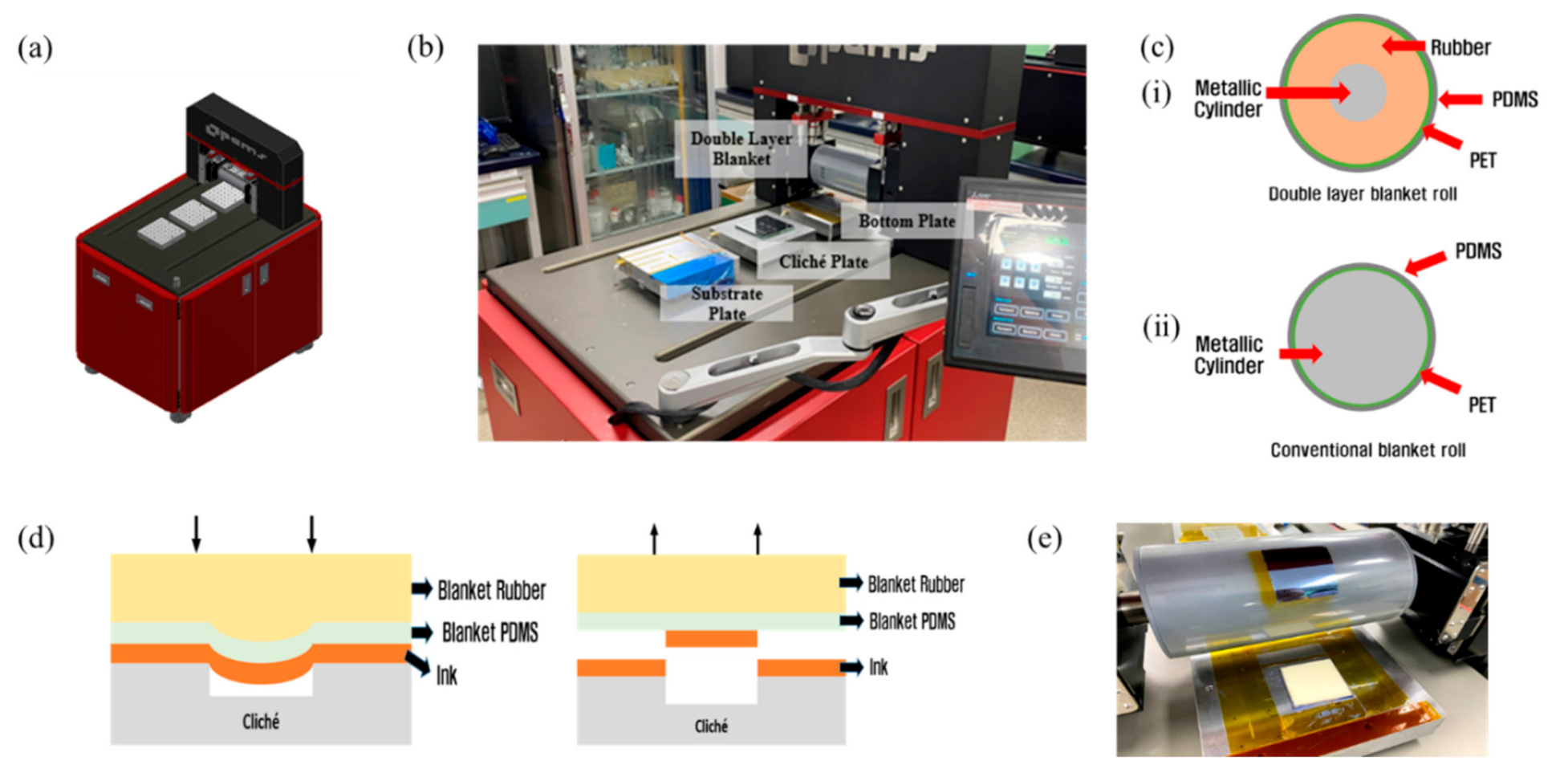
2.1. Process
2.2. DLB Reverse Offset Printer
2.3. Double-Layer Blanket (DLB) Roll
2.4. Cliché and Ink
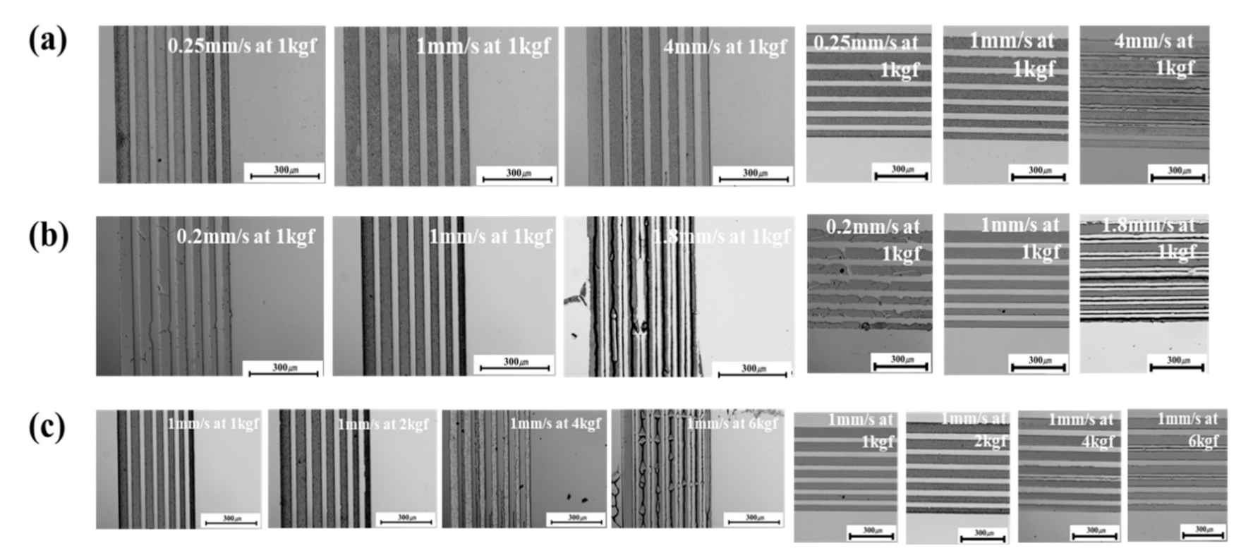
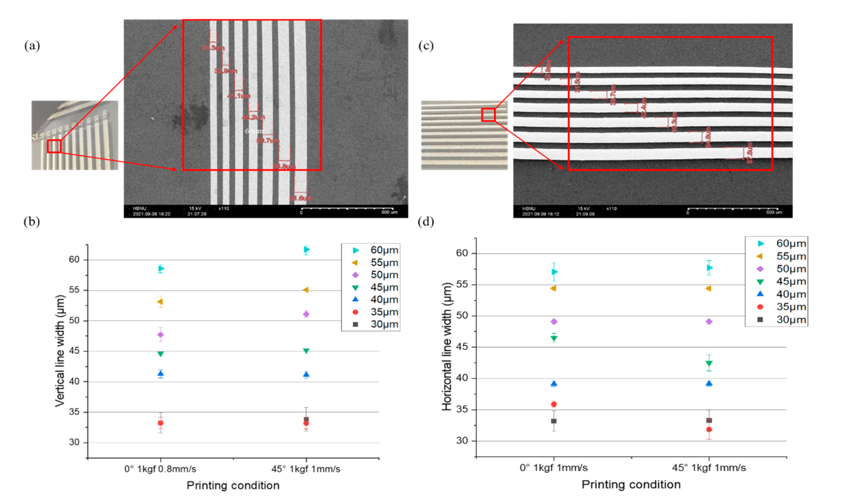
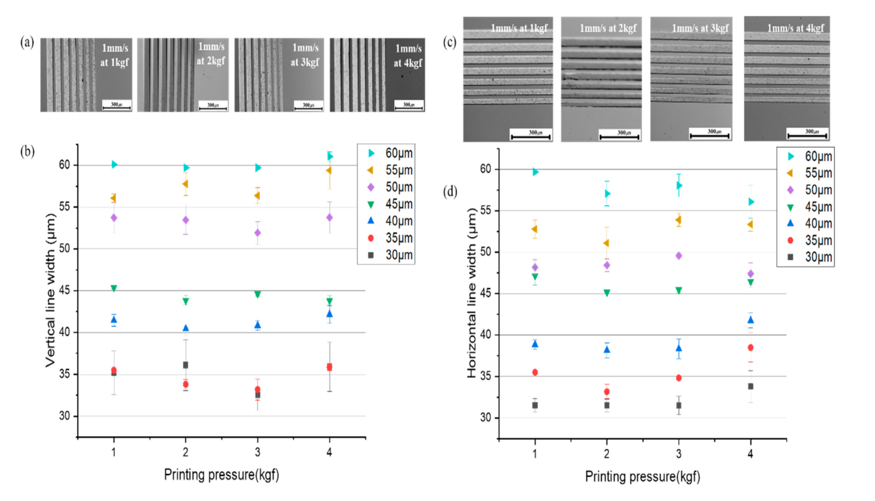
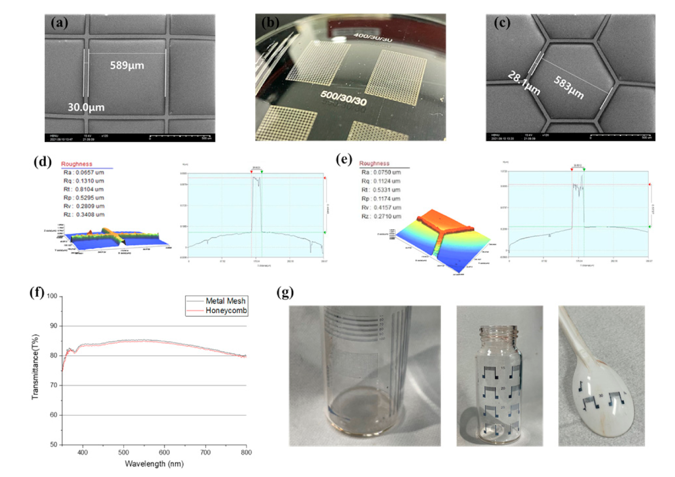
3. Result and Discussion
4. Conclusions
Supplementary Materials
Author Contributions
Funding
Institutional Review Board Statement
Informed Consent Statement
Data Availability Statement
Conflicts of Interest
References
- Dai, J.; Ogbeide, O.; Macadam, N.; Sun, Q.; Yu, W.; Li, Y.; Su, B.; Hasan, T.; Huang, X.; Huang, W. Printed gas sensors. Chem. Soc. Rev. 2020, 49, 1756–1789. [Google Scholar] [CrossRef] [PubMed]
- Noh, J.; Lee, T.; Park, S.; Jo, J.; Kim, D. Design and development of gravure offset printing system. J. Korean Soc. Precis. Eng. 2010, 27, 16–19. [Google Scholar]
- Grau, G. Gravure-Printed Electronics: Devices, Technology Development and Design; University of California; ProQuest Dissertations Publishing: Berkeley, CA, USA, 2017; ISBN 10189428. [Google Scholar]
- Lee, T.-M.; Noh, J.-H.; Kim, I.; Kim, N.-S.; Chun, S. Reliability of gravure offset printing under various printing conditions. J. Appl. Phys. 2010, 108, 102802. [Google Scholar] [CrossRef]
- Lee, T.-M.; Lee, S.-H.; Noh, J.-H.; Kim, D.-S.; Chun, S. The effect of shear force on ink transfer in gravure offset printing. J. Micromech. Microeng. 2010, 20, 125026. [Google Scholar] [CrossRef]
- Lee, T.; Kang, T.; Yang, J.; Jo, J.; Kim, K.; Choi, B. Kim, D. Drop-on-demand solder droplet jetting system for fabricating microstructure. IEEE Trans. Electron. Packag. Manuf. 2008, 31, 202–210. [Google Scholar] [CrossRef]
- Krebs, F.C. Polymer solar cell modules prepared using roll-to-roll methods: Knife-over-edge coating, slot-die coating and screen printing. Sol. Energy Mater. Sol. Cells 2009, 93, 465–475. [Google Scholar] [CrossRef]
- Lee, T.-M.; Choi, Y.-J.; Nam, S.-Y.; You, C.-W.; Na, D.-Y.; Choi, H.-C.; Shin, D.-Y.; Kim, K.-Y.; Jung, K.-I. Color filter patterned by screen printing. Thin Solid Films 2008, 516, 7875–7880. [Google Scholar] [CrossRef]
- Kang, H.-K.; Lee, C.-W.; Lee, J.-M.; Shin, K.-H. Cross direction register modeling and control in a multi-layer gravure printing. J. Mech. Sci. Technol. 2010, 24, 391–397. [Google Scholar] [CrossRef]
- Krebs, F.C. Pad printing as a film forming technique for polymer solar cells. Sol. Energy Mater. Sol. Cells 2009, 93, 484–490. [Google Scholar] [CrossRef]
- Zhong, Z.W.; Ee, J.H.; Chen, S.H.; Shan, X.C. Parametric investigation of flexographic printing processes for R2R printed electronics. Mater. Manuf. Process. 2020, 35, 564–571. [Google Scholar] [CrossRef]
- Pudas, M.; Hagberg, J.; Leppävuori, S. Gravure offset printing of polymer inks for conductors. Prog. Org. Coat. 2004, 49, 324–335. [Google Scholar] [CrossRef]
- Lee, S.; Nam, K.; Lee, T.; Yoon, D.; Jo, J. Analysis of ink transfer mechanism in gravure-offset printing process. J. Korean Soc. Precis. Eng. 2011, 28, 1146–1152. [Google Scholar]
- Lee, H.; Jang, Y. Printing Technology for Flexible Displays. Polym. Sci. Technol. 2011, 22, 237–241. [Google Scholar]
- Kusaka, Y.; Sugihara, K.; Koutake, M.; Ushijima, H. Overlay of semi-dried functional layers in offset printing for rapid and high-precision fabrication of flexible TFTs. J. Micromech. Microeng. 2014, 24, 35020. [Google Scholar] [CrossRef]
- Choi, Y.-M.; Kim, K.-Y.; Jo, J.; Lee, T.-M. Effect of PDMS Blanket Deformation on Printability in Reverse-Offset Printing. Trans. Korean Soc. Mech. Eng. B 2014, 38, 709–714. [Google Scholar] [CrossRef]
- Yoon, S.H.; Lee, J.; Lee, S.H.; Lee, B.-J.; Shin, J.-K. A Study on Processing of TFT Electrodes for Digital Signage Display using a Reverse Offset Printing. J. Korean Soc. Precis. Eng. 2014, 31, 497–504. [Google Scholar] [CrossRef] [Green Version]
- Choi, Y.-M.; Lee, E.-S.; Lee, T.-M.; Kim, K.-Y. Optimization of a reverse-offset printing process and its application to a metal mesh touch screen sensor. Microelectron. Eng. 2015, 134, 1–6. [Google Scholar] [CrossRef]
- Pudas, M.; Hagberg, J.; Leppävuori, S. Printing parameters and ink components affecting ultra-fine-line gravure-offset printing for electronics applications. J. Eur. Ceram. Soc. 2004, 24, 2943–2950. [Google Scholar] [CrossRef]
- Yang, H.; Leow, W.R.; Chen, X. 3D Printing of Flexible Electronic Devices. Small Methods 2017, 2. [Google Scholar] [CrossRef] [Green Version]
- Park, Y.; Lee, J.; Kang, S. 3D printed electronics research trend. J. Microelectron. Packag. Soc. 2021, 28, 1–12. [Google Scholar]
- Lee, T.; Choi, H.; Noh, J.; Kim, D. Pad printed PEMS device printed on a curved surface. In Proceedings of the KSME Conference, Jeongseon, Korea, 24–25 April 2008; The Korean Society of Mechanical Engineers: Jeju, Korea, 2008; pp. 1087–1090. [Google Scholar]
- Izumi, K.; Yoshida, Y.; Tokito, S. Soft blanket gravure printing technology for finely patterned conductive layers on three-dimensional or curved surfaces. Jpn. J. Appl. Phys. 2017, 56, 05EA03. [Google Scholar] [CrossRef] [Green Version]
- Izumi, K.; Yoshida, Y.; Tokito, S. Novel soft blanket gravure printing technology with an improved ink transfer process. Flex. Print. Electron. 2017, 2, 024003. [Google Scholar] [CrossRef]
- Izumi, K.; Saito, H.; Yoshida, Y.; Tokito, S.; Ushijima, H. Newly developed soft blanket reverse-offset (SBR) printing technology for forming widely patterned layers on curved surfaces. Jpn. J. Appl. Phys. 2020, 59, 031003. [Google Scholar] [CrossRef]
- Lee, H.B.; Jin, W.-Y.; Ovhal, M.M.; Kumar, N.; Kang, J.-W. Flexible transparent conducting electrodes based on metal meshes for organic optoelectronic device applications: A review. J. Mater. Chem. C 2018, 7, 1087–1110. [Google Scholar] [CrossRef]
- Choi, Y.-M.; Jo, J.; Lee, E.; Jang, Y.; Kim, I.; Park, J.H.; Yang, C.-M.; Kim, W.C.; Lee, T.-M.; Kwon, S. Reverse offset printing of transparent metal mesh electrodes using an imprinted disposable cliché. Int. J. Precis. Eng. Manuf. 2015, 16, 2347–2352. [Google Scholar] [CrossRef]
- Bae, S.W.; Kwak, S.W.; Kim, I.Y.; Noh, Y.-Y. A Study on Processing of Auxiliary Electrodes for OLED Lighting Devices Using a Reverse Gravure-Offset or Gravure-Offset Printing. J. Korean Soc. Precis. Eng. 2013, 30, 578–583. [Google Scholar] [CrossRef]
- Choi, Y.-M.; Kim, K.-Y.; Lee, E.; Jo, J.; Lee, T.-M. Fabrication of a single-layer metal-mesh touchscreen sensor using reverse-offset printing. J. Inf. Disp. 2014, 16, 37–41. [Google Scholar] [CrossRef] [Green Version]


| Specifications | DLB Reverse Offset Printer |
|---|---|
| Suction plate size/EA | 180 × 180 mm/3 EA |
| Dimension (W × H × L) | 1340 × 1120 × 830 mm |
| Accuracy | 2 μm or less |
| Printing pressure | 1–30 kgf or less |
| Printing speed | 0.1–100 mm/s |
| Substance | Stainless Steel | Rubber | PDMS |
|---|---|---|---|
| Hardness (Shore A) | - | 25 | 55 |
| Material | - | RTV | PDMS |
| Color | - | Gray | Translucent white |
| Outside diameter (thickness) | 45 mm | 120 mm | 0.68 mm |
| Form | Cylindrical roll | Roll | Sheet (on to PET film) |
| Length | 369 mm | 280 mm | 276 mm |
| Average Error Rate | 1 kgf (9.8 N) | 2 kgf (19.6 N) | 3 kgf (29.4 N) | 4 kgf (39.2 N) |
|---|---|---|---|---|
| Vertical | 4.67% | 5.70% | 3.26% | 6.10% |
| Horizontal | 3.21% | 4.35% | 2.41% | 6.17% |
Publisher’s Note: MDPI stays neutral with regard to jurisdictional claims in published maps and institutional affiliations. |
© 2022 by the authors. Licensee MDPI, Basel, Switzerland. This article is an open access article distributed under the terms and conditions of the Creative Commons Attribution (CC BY) license (https://creativecommons.org/licenses/by/4.0/).
Share and Cite
Lee, H.; Cho, N.-J.; Kim, D.-s. Development of a Novel Reverse Offset Printer Equipped with Double-Layer Blanket (DLB) for Micropattern Printing on 3D Curved Surfaces. Processes 2022, 10, 424. https://0-doi-org.brum.beds.ac.uk/10.3390/pr10020424
Lee H, Cho N-J, Kim D-s. Development of a Novel Reverse Offset Printer Equipped with Double-Layer Blanket (DLB) for Micropattern Printing on 3D Curved Surfaces. Processes. 2022; 10(2):424. https://0-doi-org.brum.beds.ac.uk/10.3390/pr10020424
Chicago/Turabian StyleLee, Hyunah, Nam-Joo Cho, and Dong-soo Kim. 2022. "Development of a Novel Reverse Offset Printer Equipped with Double-Layer Blanket (DLB) for Micropattern Printing on 3D Curved Surfaces" Processes 10, no. 2: 424. https://0-doi-org.brum.beds.ac.uk/10.3390/pr10020424