Article

Impact of Nitrogen, Boron and Phosphorus Impurities on the Electronic Structure of Diamond Probed by X-ray Spectroscopies

by
Sneha Choudhury
1,2,
Ronny Golnak
1,
Christian Schulz
1,
Klaus Lieutenant
1,
Nicolas Tranchant
3,
Jean-Charles Arnault
3,†,
Marie-Amandine Pinault-Thaury
4,
François Jomard
4,
Peter Knittel
5 and
Tristan Petit
1,*
1
Helmholtz-Zentrum Berlin für Materialen und Energie GmbH, Albert-Einstein-Str. 15, 12489 Berlin, Germany
2
Department of Chemistry, Freie Universität Berlin, Arnimallee 14, 14195 Berlin, Germany
3
CEA, LIST, Diamond Sensors Laboratory, 91191 Gif-sur-Yvette, France
4
Université Paris-Saclay, UVSQ, CNRS, GEMaC, 78000 Versailles, France
5
Fraunhofer Institute for Applied Solid State Physics, Tullastraße 72, 79108 Freiburg, Germany
*
Author to whom correspondence should be addressed.
Current address: NIMBE, UMR CEA-CNRS 3685, Université Paris-Saclay, F-91191 Gif-sur-Yvette, France.
Submission received: 12 February 2021 / Revised: 26 February 2021 / Accepted: 6 March 2021 / Published: 9 March 2021
(This article belongs to the Collection Feature Papers in the Science and Engineering of Carbons)

Abstract

:
Doping diamond with boron, nitrogen or phosphorus enables a fine tuning of its electronic properties, which is particularly relevant for applications involving electron emission. However, the chemical nature of the doping sites and its correlation with electron emission properties remain to be clarified. In this work, we applied soft X-ray spectroscopy techniques to probe occupied and unoccupied electronic states in undoped, boron-, phosphorus- and nitrogen-containing single crystal diamonds. X-ray absorption, X-ray emission and X-ray photoemission spectroscopies, performed at the carbon K-edge, provide a full picture of new electronic states created by impurities in diamond. The different probing depths of fluorescence- and electron-based detection techniques enable a comparison between surface and bulk contributions.

Graphical Abstract

1. Introduction

Diamond is a wide bandgap semiconductor with fascinating electronic properties that can be modulated by doping. As a result, it is a promising versatile material for high power electronics, electron field emission, electrochemistry or quantum computing. Diamond also has a unique ability to emit solvated electrons in water upon light illumination, which can be used to trigger chemical reactions such as CO2 or N2 reduction [1,2]. However, electron photoemission requires diamond illumination with deep UV light to overcome the diamond band gap and is therefore fairly inefficient with visible light illumination. In order to increase the diamond light absorption, nanostructuring [3,4], combination with dyes absorbing in the visible spectrum [5,6] and incorporation of metal nanoparticles to generate plasmonic effects [7] have been proposed. Incorporation of heteroatoms in the diamond matrix to add new absorption states is another approach that has also been shown to enable visible light absorption [8]. Furthermore, doping diamond with heteroatoms such as boron, nitrogen and phosphorus can tune the electron emission of the diamond as it has been thoroughly investigated over the last 25 years for electron field emission [9,10,11,12].
p-type doping of diamond is easily achieved by direct substitution of the carbon atoms by boron atoms. On the other hand, n-type doping using either nitrogen or phosphorus as dopant has turned out to be more challenging. Nitrogen, which is also present in natural types Ib and Ia diamonds, has a negative formation energy of −3.4 eV, as shown by ab initio calculations, and hence can be easily substituted in the diamond lattice [13]. However, nitrogen substitution results in distortion of the diamond lattice due to antibonding interaction between the nitrogen lone pair orbitals and carbon dangling bond [13]. Furthermore, the incorporation of nitrogen leads to the formation of deep donor levels, 1.7 eV below the conduction band minimum (CBM), which makes it insulating at room temperature [14]. Phosphorus is suitable as a donor atom due to its shallow donor level 0.56 eV below CBM. It has, however, a high formation energy of 10.4 eV, thus making it difficult to incorporate in the diamond lattice [13]. Despite these challenges, phosphorus has been incorporated in the diamond (111) layers at high concentrations [15,16]. The nature of the added absorption states in doped diamond materials remains, however, unclear and needs more detailed spectroscopic characterization.
In this work, undoped, boron-, nitrogen- and phosphorus-doped single crystal diamonds are characterized by synchrotron-based soft X-ray spectroscopies. X-ray absorption spectroscopy (XAS) at the carbon K-edge is applied using total electron yield (TEY) and partial fluorescence yield (PFY) detection modes. In the XAS process, the core electrons are resonantly excited into unoccupied electronic levels [17]. The excitation energy of the incoming X-ray can be tuned to match the different transitions observed in diamond materials, and the partial density of unoccupied states related to carbon atoms can be probed. XAS characterization of diamond in transmission is challenging as it requires sub-100 nm freestanding diamond films. Instead, TEY detection mode, based on the measurement of the drain current induced by the emission of photoelectrons and Auger electrons upon X-ray absorption, is often used. TEY is particularly surface-sensitive as the inelastic mean free path of the electrons depends on their kinetic energies, and it is typically lower than 1 nm here [18], therefore only probing the first few diamond monolayers. Alternatively, PFY based on fluorescence detection of radiative decay processes can also be used to detect XAS. In this case, the diamond materials are probed deeper as the attenuation length of X-ray photons at the carbon K-edge is lower than 60 nm [19]. Another advantage of PFY-XAS is that it can be applied to insulating materials, while TEY-XAS requires a surface-conductive sample.
As a result, X-ray emission spectroscopy (XES) and X-ray photoemission spectroscopy (XPS) are used to characterize the occupied states of the diamond materials. XES is obtained by analyzing the energy of X-ray photons decaying into the core hole generated after non-resonant X-ray excitation above the carbon K-edge. This method probes the partial density of occupied electronic states in the valence band. It is highly complementary to XPS, which can also probe valence states but without element-sensitivity and with a higher surface sensitivity due to the electron detection. The combination of photon-in–electron-out (TEY-XAS and XPS) and photon-out (PFY-XAS and XES) methods ensures surface and bulk sensitivity, respectively. By comparing these different detection methods, the influence of diamond doping on the surface and bulk diamond electronic structures is discussed.

2. Materials and Methods

2.1. Diamond Materials

Undoped diamond (uSCD): An undoped substrate with <111> orientation obtained from Diam2Tec (Germany) was used.
B-doped diamond (B-SCD): Boron-doped <111> substrate, obtained from the Technological Institute for Superhard Materials (TISNCM, Russia) was used. The boron concentration extracted from the secondary ion mass spectrometry (SIMS) profile was 2.7 × 10²⁰ atoms/cm3, i.e., ~1500 ppm (see Supplementary Information).
P-doped diamond (P-SCD): P-doped overgrowth was conducted on undoped <111> substrates (Diam2Tec, Germany). The same cleaning treatment as the B-doped diamond was used. The P-doped epilayer was grown in an ellipsoidal microwave plasma chemical vapor deposition (MPCVD) reactor using purified source gases (H2, CH4) and trimethylphosphine (diluted, P(CH3)3/H2 = 4500 ppm) at a gas pressure of 190 mbar [20]. The microwave power was 2.1 kW. The growth was conducted at a CH4 to H2 ratio of 0.13% and a P to C ratio of 20% using a growth temperature of approximately 1000 °C. The phosphorus concentration extracted from the SIMS profile was 8 × 10¹⁹ atoms/cm3, i.e., ~400 ppm (see Supplementary Information).
N-doped diamond (N-SCD): A nitrogen-doped diamond epilayer was grown by microwave plasma CVD onto an HPHT <100> Sumitomo substrate after an acid cleaning of its surface. The MPCVD growth used a gas mixture composed of hydrogen 95 vol%, methane 4 vol% and nitrogen 1 vol% with a total gas flow of 202 standard cubic centimeters per minute (SCCM) and a gas pressure of 100 mbar. The applied microwave power was 630 W and the duration of growth was 300 min at a temperature of approximately 900 °C. The epilayer thickness measured by SIMS was 19 microns, corresponding to a growth rate of 3–4 microns per hour. The nitrogen concentration extracted from the SIMS profile was 4.9 × 10¹⁸ atoms/cm3, i.e., ~30 ppm (see Supplementary Information).
All samples were used for spectroscopic study after thorough cleaning in a mixture of sulfuric and nitric acid (ratio 3:1) for 1.5 h at a hotplate temperature of 250 °C, followed by surface hydrogenation carried out in an H2 plasma at 750 °C for 30 min in the MPCVD reactor. The samples were not polished before characterization.

2.2. Secondary Ion Mass Spectrometry Analysis

SIMS was performed in order to measure the depth distribution of the boron ([B]), phosphorus ([P]) and nitrogen ([N]) concentrations in B-SCD, P-SCD and N-SCD samples, respectively. Prior to SIMS analysis, a gold film of ~50 nm was deposited to avoid any charging effects during measurements. CAMECA IMS7f equipment was used. The vacuum limit reached in the analysis chamber was of ∼10−9 mbar. The depth of the resulting 150 × 150 µm2 SIMS crater was measured using a Dektak8 step-meter. The analyzed zone was restricted to a diameter of 33 µm to limit the crater edge effects. Further experimental details are available in the Supplementary Information.

2.3. Differential Interference Contrast Microscopy

Differential interference contrast (DIC) microscopy was performed on doped samples at GEMaC with a Nikon ECLIPSE ME600L microscope. B-SCD and P-SCD were imaged before SIMS analysis, unlike the N-SCD sample. For this reason, SIMS craters (squares) resulting from the N content analysis were visible on the N-SCD surface.

2.4. X-ray Absorption Spectroscopy

XAS measurements were performed at the U49/2-PGM1 undulator beamline of the synchrotron BESSY II using the LiXEdrom end-station. The TEY-XAS were recorded by measuring the drain photocurrent through the sample holder. The PFY-XAS were recorded using an X-ray spectrometer with a Rowland circle geometry. The XA spectra were energy calibrated to the diamond second bandgap located at 302.4 eV.

2.5. X-ray Emission and Photoemission Spectroscopies

XES, valence band XPS and Resonant Photoemission Spectroscopy (RPES) were recorded at the U41-PGM undulator beamline of the synchrotron BESSY II using the PEAXIS end-station [21]. The samples were annealed at 250 °C for 1 h before characterization. The energy calibration for XES was performed using the elastic emission line of the B-SCD sample.

3. Results

3.1. Electronic States of Diamond Probed by XAS and XES at the C K-Edge

The XAS and XES at the carbon K-edge provide a full picture of the partial electronic density of states as shown for undoped (111) single crystal diamond (uSCD) in Figure 1. Characteristic XAS features of diamond materials [22] such as the large bandgap, the sharp core excitonic peak at 289.3 eV and the second bandgap at 302.4 eV, are clearly distinguished in Figure 1. The conduction band maximum (CBM) was estimated at 289.5 eV, considering that the core exciton has a binding energy of approximately 0.2 eV [22]. XES of diamond materials presents a large band between 274–284 eV related to 2p states while 2s states appear as a smaller band around 271.3 eV [23]. The energy onset at 284.0 eV corresponds to the valence band maximum (VBM). The difference between the VBM obtained from XES and CBM from XAS agreed well with a diamond bandgap of 5.5 eV. Electronic states observed in between were related to defect-related sub-bandgap states. In the following, we will investigate how these features are modified by incorporation of boron, nitrogen or phosphorus impurities in the diamond lattice.

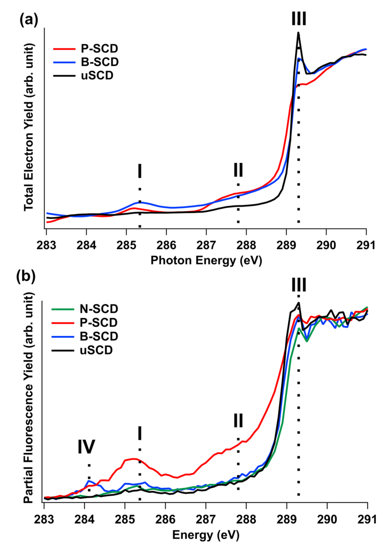
3.2. Unoccupied Electronic States of Doped Diamond

The B-, P- and N-doped samples were prepared by MPCVD as detailed in the experimental section and respectively labeled B-SCD, P-SCD and N-SCD. The morphology of the different doped samples was imaged by DIC microscopy (Figure S1). B-SCD presented a smooth surface while the surface of P-SCD sample was rough with some straight marks. The N-SCD surface was partly covered by typical hillocks with unepitaxial crystallites on top of them. The doping concentration was measured by SIMS over 300 nm, which is deeper than the probing depth of X-ray spectroscopy techniques, as detailed in the Supplementary Information. For the B-SCD and N-SCD samples, the impurity concentrations were constant with plateaus of [B] ~2.7 × 10²⁰ at/cm3 and [N] ~4.9 × 10¹⁸ at/cm3, respectively. The phosphorus content of P-SCD sample presented a weak increase in the first 150 nm by a factor ~1.5 in the content up to a plateau of [P] ~8.0 × 10¹⁹ at/cm3 (Figure S3). These doping concentrations were relatively high in order to increase the number of defect states induced by heteroatoms for sub-bandgap absorption. Note, however, that the doping was performed independent of the conductivity of the samples.
The modification of the unoccupied electronic states in the diamond bandgap by doping is first described. TEY-XAS of uSCD, B-SCD and P-SCD are presented in Figure 2a. The main C K-edge is situated around 290 eV and the discussion is focused on the sub-bandgap region (283–290 eV), relevant for visible light absorption. The TEY-XAS of the N-doped sample is not shown here because of the different crystal orientation compared to the other diamond samples. As a result, different surface electronic states could not be directly related to nitrogen heteroatoms, and we will then limit the discussion to PFY-XAS for N-SCD in the following.
On TEY-XAS, three features I, II and III at 285.3, 287.6 and 289.3 eV, respectively, can be distinguished. The peak I related to 𝜋* transitions from sp2-hybridized carbon atoms is more intense for doped samples. The peak II usually attributed to C-H termination on the diamond was also found to have an increased absorption for P-SCD and B-SCD [24]. Finally, the peak III is related to the core excitons in the diamond [22]. This core excitonic peak appears very sharp for uSCD and is slightly broadened for B-SCD. On P-SCD, this peak almost vanishes, illustrating a strong sensitivity of the excitonic peak to impurity incorporation. For nanocrystalline diamond, this was previously interpreted as a reduction of short-range order within the sample due to defects introduced upon impurity incorporation [25]. Heteroatom incorporation, therefore, also affected the core excitons in single crystal diamond. In addition, the rising edge appears shifted below 289 eV for P-SCD. Impurity levels induced by substitutional phosphorus located 0.56 eV below the CBM may contribute to the broadened excitonic peak and decrease of the rising C K-edge for P-SCD [26,27].
Interestingly, PFY-XAS of the doped diamond samples are slightly different (Figure 2b). A new feature IV appears on B-SCD at 284.1 eV, which was previously shown to be related to B-induced defects [3,28]. On P-SCD, the features I and II have a significant contribution compared to uSCD. Since PFY-XAS is bulk-sensitive, it demonstrates that this contribution comes from sp2 bonds and C-H groups, not only on the diamond surface but also incorporated in the diamond matrix. This may result from the large size of phosphorus atoms compared to the carbon atoms, therefore leading to defect formation upon doping. Many different defects sites are possible in P-SCD, related to different levels of H incorporation, which can lead to the broadening of the feature II [29]. For N-SCD, no strong differences were observed compared to uSCD except a relative decrease of the excitonic peak III. This latter had a lower relative intensity for the three doped samples, compared to uSCD.

3.3. Occupied Electronic States of Doped Diamond

The role of doping on the occupied electronic states was then characterized. The XES spectra of the B-SCD, N-SCD and P-SCD samples appear similar to the XES of uSCD (Figure 3a). As mentioned earlier, a large band between 274–284 eV (features B, C and D) is related to 2p states, while 2s states appear as a smaller band around 271.3 eV (feature E) [23]. Since XES is bulk-sensitive and probes only carbon atoms, it was not strongly altered by the impurity concentration of the diamond samples investigated here.
On the other hand, significant modifications of the valence band measured by XPS can be observed. Two different excitation energies (299 and 200 eV) were used. At 299 eV excitation (Figure 3b), carbon atoms are resonantly excited, therefore their X-ray cross-section is enhanced compared to other elements. At 200 eV excitation energy (Figure 3c), all atoms are excited, therefore contribution from dopants and eventual oxygen groups remaining on the diamond surface are also expected. Note that no photoelectrons were detected from N-SCD, probably as a result of a poor electrical conduction of the sample due to a high nitrogen defect density. As mentioned earlier, this sample having a different crystal orientation, a direct comparison to the other doped samples was not possible. A strong charging effect was observed for P-SCD, which may also have suffered from a poor conduction. However, photoelectrons were still observed for the P-SCD sample and the charging effect could be corrected using the resonant C1s signal (see Supplementary Information). Further XPS spectra at different resonant excitations are shown in Figure S4.
The non-resonant diamond valence band of uSCD (Figure 3c) is constituted of four main bands at 6.7 eV, 12.5 eV, 17.6 eV and 24.5 eV. The band at 6.7 eV was related to C2p electrons, while the next two features were related to C2s states of sp3-hybridized carbon [23]. The last feature at 24.5 eV was tentatively attributed to O2s core electrons coming for residual oxygen groups on the diamond surface [30]. A small shoulder at 286.0 eV was indeed observed at the C1s, which could be related to C-OH groups (Figure S4). The C2p peak corresponding to the feature C from the XES, seemed the most affected by impurities incorporation as its maximum shifted by –1.3 eV (+1.9 eV) for B-SCD (P-SCD) compared to uSCD. It is also sharper (broader) for B-SCD (P-SCD). This may have resulted from a higher localization of electrons in B-SCD as compared to uSCD. However, the cross-section of photoelectrons coming from boron atoms may also have been enhanced at 200 eV as the boron signature at the B K-edge was found at 193.8 eV (Figure 4). On the other hand, P-SCD leads to more delocalized electronic states, resulting in broader spectral features. A stronger signal from electrons with a binding energy below 3 eV was observed for P-SCD, possibly related to electron donor states.
The resonant valence band spectra at 299 eV (Figure 3b) show a slightly different picture. Features around 2–3 eV binding energy are significantly enhanced for B- and P-SCD samples compared to non-resonant spectra and undoped diamond. These occupied electronic states were most likely related to surface reconstructions [30], which were possibly induced by distortion of the diamond lattice upon doping and growth ending. This agreed with the small sp2 carbon content observed from XAS (Figure 2).
Note that the diamond surface states are highly sensitive to surface chemistry, crystal orientation, surface roughness, polishing treatment and doping concentration, to name a few parameters. Photon-in–electron-out techniques are highly sensitive to these surface states because the inelastic mean free path of photoelectrons is below 1 nm for the kinetic energy range applied here. The high impurity concentrations of the investigated sample may also have led to dopant clustering and local inhomogeneities, the detailed investigation of which was beyond the scope of this study. While this work gives insights into the effect of impurity incorporation on the changes of electronic states on H-terminated single crystal diamond, further studies on differently prepared diamond samples are clearly required before generalizing these results to all B-, P- and N-doped diamond samples.

4. Conclusions

In this work, the electronic structure of single crystal diamonds containing boron, nitrogen and phosphorus were compared by means of soft X-ray absorption, emission and photoemission spectroscopies. New unoccupied electronic states were observed for B-SCD and P-SCD close to the CBM and VBM, respectively, as determined by PFY-XAS. In addition, the incorporation of B, P and N atoms was found to reduce significantly the diamond core exciton contribution compared to undoped diamond in both TEY- and PFY-XAS. Occupied electronic states were not significantly modified by B, P or N addition as estimated from XES for the investigated heteroatom concentration. On the other hand, the surface occupied electronic states were strongly affected by impurities, and the presence of surface reconstruction was evidenced for both B-SCD and P-SCD using XPS of the valence band. Overall, this study illustrates how complementary photon-out and electron-out X-ray spectroscopies can be used for the comprehensive characterization of diamond materials.

Supplementary Materials

The following are available online at https://0-www-mdpi-com.brum.beds.ac.uk/2311-5629/7/1/28/s1, Figure S1: Differential interference contrast (DIC) microscopy of diamond samples, Figure S2: Mass spectra of N-doped diamond, Figure S3: Secondary ion mass spectrometry (SIMS) profiles of doped diamond samples, Figure S4: XPS C1s of diamond samples, Figure S5: RPES at the valence band of doped diamond samples.

Author Contributions

Conceptualization, S.C. and T.P.; sample preparation, N.T., J.-C.A., P.K.; XAS experiments, S.C., R.G., T.P.; XES and XPS experiments, S.C., C.S., K.L., T.P.; SIMS and DIC experiments, M.-A.P.-T., F.J.; writing, S.C., T.P. with comments from all authors; supervision, T.P.; All authors have read and agreed to the published version of the manuscript.

Funding

This research was funded by the European Union’s Horizon 2020 Program under Grant Agreement number 665085 (DIACAT). The APC was funded by HZB.

Acknowledgments

We thank Christoph Nebel for his comments on the manuscript. We acknowledge the kind support by staff members of the BESSY II Synchrotron Facility. We thank HZB for the allocation of synchrotron radiation beamtime.

Conflicts of Interest

The authors declare no conflict of interest.

References

  1. Zhu, D.; Zhang, L.; Ruther, R.E.; Hamers, R.J. Photo-illuminated diamond as a solid-state source of solvated electrons in water for nitrogen reduction. Nat. Mater. 2013, 12, 836–841. [Google Scholar] [CrossRef] [PubMed]
  2. Zhang, L.; Zhu, D.; Nathanson, G.M.; Hamers, R.J. Selective Photoelectrochemical Reduction of Aqueous CO2 to CO by Solvated Electrons. Angew. Chem. Int. Ed. 2014, 53, 9746–9750. [Google Scholar] [CrossRef]
  3. Choudhury, S.; Kiendl, B.; Ren, J.; Gao, F.; Knittel, P.; Nebel, C.; Venerosy, A.; Girard, H.; Arnault, J.-C.; Krueger, A.; et al. Combining nanostructuration with boron doping to alter sub band gap acceptor states in diamond materials. J. Mater. Chem. A 2018, 6, 16645–16654. [Google Scholar] [CrossRef] [Green Version]
  4. Knittel, P.; Buchner, F.; Hadzifejzovic, E.; Giese, C.; Quellmalz, P.; Seidel, R.; Petit, T.; Iliev, B.; Schubert, T.J.S.; Nebel, C.E.; et al. Nanostructured Boron Doped Diamond Electrodes with Increased Reactivity for Solar-Driven CO2 Reduction in Room Temperature Ionic Liquids. ChemCatChem 2020, 12, 5548–5557. [Google Scholar] [CrossRef]
  5. Zegkinoglou, I.; Cook, P.L.; Johnson, P.S.; Yang, W.; Guo, J.; Pickup, D.; González-Moreno, R.; Rogero, C.; Ruther, R.E.; Rigsby, M.L.; et al. Electronic Structure of Diamond Surfaces Functionalized by Ru(tpy)2. J. Phys. Chem. C 2012, 116, 13877–13883. [Google Scholar] [CrossRef]
  6. Yeap, W.S.; Liu, X.; Bevk, D.; Pasquarelli, A.; Lutsen, L.; Fahlman, M.; Maes, W.; Haenen, K. Functionalization of Boron-Doped Nanocrystalline Diamond with N3 Dye Molecules. ACS Appl. Mater. Interfaces 2014, 6, 10322–10329. [Google Scholar] [CrossRef] [PubMed] [Green Version]
  7. Li, S.; Bandy, J.A.; Hamers, R.J. Enhanced Photocatalytic Activity of Diamond Thin Films Using Embedded Ag Nanoparticles. ACS Appl. Mater. Interfaces 2018, 10, 5395–5403. [Google Scholar] [CrossRef] [PubMed]
  8. Sun, T.; Koeck, F.A.M.; Zhu, C.; Nemanich, R.J. Combined visible light photo-emission and low temperature thermionic emission from nitrogen doped diamond films. Appl. Phys. Lett. 2011, 99, 202101. [Google Scholar] [CrossRef]
  9. Zhu, W.; Kochanski, G.P.; Jin, S.; Seibles, L. Defect-enhanced electron field emission from chemical vapor deposited diamond. J. Appl. Phys. 1995, 78, 2707–2711. [Google Scholar] [CrossRef]
  10. Geis, M.W.; Twichell, J.C.; Efremow, N.N.; Krohn, K.; Lyszczarz, T.M. Comparison of electric field emission from nitrogen-doped, type Ib diamond, and boron-doped diamond. Appl. Phys. Lett. 1996, 68, 2294–2296. [Google Scholar] [CrossRef]
  11. Lacher, F.; Wild, C.; Behr, D.; Koidl, P. Electron field emission from thin fine-grained CVD diamond films. Diam. Relat. Mater. 1997, 6, 1111–1116. [Google Scholar] [CrossRef]
  12. Yamada, T.; Okano, K.; Yamaguchi, H.; Kato, H.; Shikata, S.-I.; Nebel, C.E. Field emission from reconstructed heavily phosphorus-doped homoepitaxial diamond (111). Appl. Phys. Lett. 2006, 88, 212114. [Google Scholar] [CrossRef]
  13. Kajihara, S.A.; Antonelli, A.; Bernholc, J.; Car, R. Nitrogen and potential n-type dopants in diamond. Phys. Rev. Lett. 1991, 66, 2010–2013. [Google Scholar] [CrossRef] [PubMed]
  14. Mort, J.; Machonkin, M.A.; Okumura, K. Compensation effects in nitrogen-doped diamond thin films. Appl. Phys. Lett. 1991, 59, 3148–3150. [Google Scholar] [CrossRef]
  15. Kato, H.; Takeuchi, D.; Ogura, M.; Yamada, T.; Kataoka, M.; Kimura, Y.; Sobue, S.; Nebel, C.E.; Yamasaki, S. Heavily phosphorus-doped nano-crystalline diamond electrode for thermionic emission application. Diam. Relat. Mater. 2016, 63, 165–168. [Google Scholar] [CrossRef] [Green Version]
  16. Grotjohn, T.; Tran, D.; Yaran, M.; Demlow, S.N.; Schuelke, T. Heavy phosphorus doping by epitaxial growth on the (111) diamond surface. Diam. Relat. Mater. 2014, 44, 129–133. [Google Scholar] [CrossRef]
  17. De Groot, F.; Kotani, A. Core Level Spectroscopy of Solids; CRC Press: Boca Raton, FL, USA, 2008. [Google Scholar]
  18. Tanuma, S.; Powell, C.J.; Penn, D.R. Calculations of electron inelastic mean free paths. IX. Data for 41 elemental solids over the 50 eV to 30 keV range. Surf. Interface Anal. 2011, 43, 689–713. [Google Scholar] [CrossRef]
  19. Henke, B.; Gullikson, E.; Davis, J. X-Ray Interactions: Photoabsorption, Scattering, Transmission, and Reflection at E = 50-30,000 eV, Z = 1–92. At. Data Nucl. Data Tables 1993, 54, 181–342. [Google Scholar] [CrossRef] [Green Version]
  20. Füner, M.; Wild, C.; Koidl, P. Novel microwave plasma reactor for diamond synthesis. Appl. Phys. Lett. 1998, 72, 1149–1151. [Google Scholar] [CrossRef]
  21. Schulz, C.; Lieutenant, K.; Xiao, J.; Hofmann, T.; Wong, D.; Habicht, K. Characterization of the soft X-ray spectrometer PEAXIS at BESSY II. J. Synchrotron Radiat. 2020, 27, 238–249. [Google Scholar] [CrossRef] [PubMed] [Green Version]
  22. Morar, J.F.; Himpsel, F.J.; Hollinger, G.; Hughes, G.; Jordan, J.L. Observation of a C- 1s Core Exciton in Diamond. Phys. Rev. Lett. 1985, 54, 1960–1963. [Google Scholar] [CrossRef] [PubMed]
  23. Endo, K.; Koizumi, S.; Otsuka, T.; Suhara, M.; Morohasi, T.; Kurmaev, E.Z.; Chong, D.P. Analysis of XPS and XES of diamond and graphite by DFT calculations using model molecules. J. Comput. Chem. 2000, 22, 102–108. [Google Scholar] [CrossRef]
  24. Graupner, R.; Ristein, J.; Ley, L.; Jung, C. Surface-sensitive K-edge absorption spectroscopy on clean and hydrogen-terminated diamond (111) and (100) surfaces. Phys. Rev. B 1999, 60, 17023–17029. [Google Scholar] [CrossRef]
  25. Birrell, J.; Gerbi, J.E.; Auciello, O.; Gibson, J.M.; Gruen, D.M.; Carlisle, J.A. Bonding structure in nitrogen doped ultrananocrystalline diamond. J. Appl. Phys. 2003, 93, 5606–5612. [Google Scholar] [CrossRef]
  26. Haenen, K.; Nesládek, M.; De Schepper, L.; Kravets, R.; Vaněček, M.; Koizumi, S. The phosphorous level fine structure in homoepitaxial and polycrystalline n-type CVD diamond. Diam. Relat. Mater. 2004, 13, 2041–2045. [Google Scholar] [CrossRef]
  27. Alfieri, G.; Kranz, L.; Mihaila, A. Phosphorus-Related Complexes and Shallow Doping in Diamond. Phys. Status Solidi (RRL) Rapid Res. Lett. 2018, 12, 1700409. [Google Scholar] [CrossRef]
  28. Nakamura, J.; Kabasawa, E.; Yamada, N.; Einaga, Y.; Saito, D.; Isshiki, H.; Yugo, S.; Perera, R.C.C. Electronic structures of B2p and C2p levels in boron-doped diamond films studied using soft X-ray absorption and emission spectroscopy. Phys. Rev. B 2004, 70, 245111. [Google Scholar] [CrossRef] [Green Version]
  29. Shikata, S.; Yamaguchi, K.; Fujiwara, A.; Tamenori, Y.; Tsuruta, K.; Yamada, T.; Nicley, S.S.; Haenen, K.; Koizumi, S. X-ray absorption near edge structure and extended X-ray absorption fine structure studies of P doped (111) diamond. Diam. Relat. Mater. 2020, 105, 107769. [Google Scholar] [CrossRef]
  30. Francz, G.; Oelhafen, P. Valence band spectroscopy of reconstructed (100) and (111) natural diamond. Diam. Relat. Mater. 1995, 4, 539–543. [Google Scholar] [CrossRef]
Figure 1. Total electron yield-X-ray absorption spectroscopy (TEY-XAS) (right) and X-ray emission spectroscopy (XES) (left) at the C K-edge of undoped single crystal diamond (uSCD). The diamond bandgaps are highlighted.
Carbon 07 00028 g001
Figure 2. (a) TEY-XAS and (b) partial fluorescence yield-X-ray absorption spectroscopy (PFY-XAS) at the carbon K-edge of uSCD (black), B-doped diamond (B-SCD) (blue), P-doped diamond (P-SCD) (red) and N-doped diamond (N-SCD) (green) samples. The XA spectra were normalized to the main edge above 290 eV.
Carbon 07 00028 g002
Figure 3. (a) XES at the C K-edge of uSCD, B-SCD, P-SCD and N-SCD recorded at 320 eV excitation energy. X-ray photoemission spectroscopy (XPS) of uSCD, B-SCD and P-SCD measured with 299 eV (b) and 200 eV (c) excitation energies. XES were normalized to the peak at 280.5 eV and XPS to the signal at 18 eV (b) and 30 eV (c). XES and XPS valence band spectra were plotted on a similar energy scale, aligning the valence band maximum from XES to the Fermi edge obtained from XPS, to facilitate comparison between the different techniques.
Carbon 07 00028 g003
Figure 4. XAS at the B K-edge on the B-SCD sample.
Carbon 07 00028 g004
Publisher’s Note: MDPI stays neutral with regard to jurisdictional claims in published maps and institutional affiliations.

