

Degree of Polarization of Cathodoluminescence from a (100) GaAs Substrate with SiN Stripes

1
Department of Engineering Physics, McMaster University, Hamilton, ON L8S 4L7, Canada
2
3SP Technologies, Route de Villejuste, F-91625 Nozay, CEDEX, France
*
Author to whom correspondence should be addressed.
Optics 2024, 5(1), 11-43; https://0-doi-org.brum.beds.ac.uk/10.3390/opt5010002
Submission received: 30 September 2023
/
Revised: 23 November 2023
/
Accepted: 9 January 2024
/
Published: 17 January 2024
(This article belongs to the Special Issue Strain in III–V Materials and Devices: Methods for Estimation and Effects)
Abstract
:Notes on fits of analytic estimations, 2D finite element method (FEM), and 3D FEM simulations to measurements of the cathodoluminescence (CL) and to the degree of polarization (DOP) of the CL from the top surface of a GaAs substrate with a 6.22 m wide SiN stripe are presented. Three interesting features are found in the DOP of CL data. Presumably these features are noticeable owing to the spatial resolution of the CL measurement system. Comparisons of both strain and spatial resolutions obtained by CL and photoluminescence (PL) systems are presented. The width of the central feature in the measured DOP is less than the width of the SiN, as measured from the CL. This suggests horizontal cracks or de-laminations into each side of the SiN of about 0.7 m. In addition, it appears that deformed regions of widths of ≈1.5 m and adjacent to the SiN must exist to explain some of the features.
1. Introduction
Waveguides in III-V materials, which include multi-mode interference (MMI) structures and lasers, might be designed with small refractive index differences, which makes the performance of these waveguide structures sensitive to the effects of a spatially varying strain [1,2,3,4,5]. The refractive index of a material, through the photo-elastic effect, is a function of strain in the material [6] (pp. 241–252).
For GaAs, and in a facet coordinate system where ‘3’ is the growth direction, ‘2’ is a normal to a cleaved facet, and ‘1’ is in the plane of the facet, changes in the refractive indices , , and owing to strains , , and are given by [7]
with
At , ; ; are elasto-optical coefficients for GaAs in a crystal coordinate system, and is the refractive index of the unstressed GaAs crystal [8,9,10,11]. The elasto-optical coefficients and refractive index are functions of wavelength, with the wavelength dependence being more pronounced near the band-gap, as expected from the Kramers–Kronig relations [12] (pp. 363–364).
The are the elasto-optical coefficients in a matrix form, and relate strain to changes in the relative dielectric impermeability tensor B, from which changes in the refractive index can be deduced. The piezo-optical coefficients, in a matrix form, relate changes in B to the applied stress. Both the piezo-optical and elasto-optical coefficients are fourth rank tensors, similar to the compliance and stiffness tensors that relate stress and strain. One can work with the and strain, or the and stress, or one can use the compliance or stiffness to relate to [6] (p. 244).
For light travelling along the ‘2’ direction, two orthogonal polarizations are along the ‘1’ and ‘3’ directions. By convention, one of these polarizations would be designated as the TE polarization and the other would be designated the TM polarization.
For simplicity, shear strains have been set equal to zero in the matrices of Equation (1). Shear strain causes a rotation of the principal axes of the indicatrix and thus leads to rotation of the plane of polarization of light for linearly polarized light propagating in regions of shear strain [7]. Soldering a chip to a carrier, i.e., die attach, causes shear strain near the edges of the chip; see Figure 1 of Ref. [7]. Laser emitters in regions of appreciable shear have been shown to emit less power than emitters in the center of the chip, where the shear strain is zero or small [13,14,15,16,17,18]. This reduction in power for emitters in regions of appreciable shear strain can be explained by birefringence owing to the presence of shear strain [7,17,18,19].
Given for GaAs and an uniaxial strain , . Thus, the strain-induced change in refractive index is of the order of the magnitude of the strain. Changes in strain near waveguides must be kept significantly below the refractive index difference that creates the waveguide, or the waveguide must be designed to use the refractive index difference caused by the strain.
Most devices include dielectric and metal overlayers, and these overlayers introduce strain [1]. Strain, particularly shear strain, which is a measure of tilting of the lattice planes [6] (p. 102), might also affect the operational lifetime of a device [20]. Unfortunately, strain from overlayers is not always easy to predict or control, as the overlayers might not be conformal or stochiometric over features such as layers, ridges, or trenches that create devices.
Thus, it is useful for understanding the operation of III-V optical devices to have methods to provide estimates of strain fields with spatial resolution that is commensurate with the scale of the features that define the optical device. One method to estimate strain in III-V devices and materials is through measurement and analysis of the degree of polarization (DOP) of luminescence from the devices and materials.
The DOP of photoluminescence (PL) is a sensitive function of the strain and is a relatively straightforward quantity to measure [21,22,23]. We measure the DOP of luminescence as , where and are the detected powers in two orthogonal polarizations for luminescence that is emitted perpendicular to the surface of the luminescent material. We also measure the rotated degree of polarization (ROP) of luminescence as , where and are obtained by a 45 deg rotation of the - measurement system about the normal to the surface [24].
This paper is concerned with measurement of the DOP of cathodoluminescence (CL) [25,26] from the surface of a GaAs substrate that has a m SiN stripe on the surface. The SiN stripe deforms the GaAs and gives rise to a strain-dependent DOP of luminescence from the GaAs, which can be measured and analyzed.
Most previous work has been analysis of the DOP of PL or electroluminescence [13,17,27,28,29,30,31,32,33,34]. CL offers better spatial resolution than PL. Three features of interest, labelled as ‘a’, ‘b’, and ‘c’, are identified in the measurements of the DOP of the CL from the (100) surface of the SiN/GaAs sample. Simulations, both analytic and finite element method (FEM), are fit to the DOP measurements and are used to explain the observed features. Where possible, comparisons of CL results with results typical of a PL system are given.
1.1. DOP Strain Dependence
For GaAs or InP, and for a standard measurement of the degree of polarization of luminescence (DOP) from the top surface (i.e., from a surface, with measurement axes oriented along and directions and for the luminescence propagating along the normal to the surface),
and
which are the same expressions for the DOP and rotated degree of polarization (ROP) as for an isotropic medium [35]. The normal to the surface or growth direction is taken as a or ‘3’ direction or direction, the normal to the cleaved facet is taken as a or or ‘2’ direction, and the remaining direction is taken as the ‘1’ or direction (i.e., a direction). The long axis of the SiN stripe runs along the direction and is perpendicular to the major flat of the wafer. The 100 subscript on and on identifies the normal of the surface under study and the direction of propagation of the luminescence under analysis. is a calibration constant and is expected to have a value of 58 [35] (Equation (26)). The strain dependencies of the DOP and of the ROP are based on Bahder’s analytic expressions for the band dispersions of strained zinc-blended crystals [36,37,38].
, , and are the principal components of strain in a Voigt or matrix notation, and in general are functions of position. is a tensor shear strain in a Voigt notation, and also in general, a function of position. The tensor components are written in a Voigt notation to reduce the number of subscripts. From Equations (4) and (5), the ROP of luminescence propagating along a direction and from a small volume located at is proportional to the shear strain at , and the DOP of luminescence propagating along a direction and from a volume element at is proportional to the difference of the principal strains at .
1.2. Preview
Section 2 provides information on the production of the SiN films and on the CL measurements. The three features of interest in the DOP data, features ‘a’, ‘b’, and ‘c’, are identified in this section. Production of CL is slightly different than the production of luminescence by photo-pumping (i.e., by photoluminescence (PL)). As a result, subsections on electron range and power deposition in the pumping process are presented for CL and are compared to PL.
The width of the SiN stripe as determined by fits of error functions to the CL yield is presented in Section 3. The fits provide a precise value for the width of the SiN stripe. Interestingly, fits of simulations to the DOP data give a width that is ≈1.4 m less than the m width as determined from fits of error functions to the CL yield. In addition to fits to the CL yield, the minimum detectable changes in DOP and the spatial resolution for the CL measurements are given and compared to corresponding values obtained by a PL measurement system. The effect of the spatial resolution of the measurement system on the simulations and on the ability to see the three features of interest is presented.
Section 4 provides background on an inclined edge-force model for strain caused by the SiN film. Fits of DOP predictions from the inclined edge-force model to the DOP data are presented. The inclined force model is an analytic model, and as such, results are obtained quickly. Results from the inclined edge-force model are used to explain the ‘a’, ‘b’, and ‘c’ features in the DOP data and are used to provide initial guesses for fits of FEM simulations to the data, which are given in the following sections.
Section 5 provides information on fits of 2D FEM simulations of the DOP to the data. Section 6 presents fits of 3D FEM simulations to the DOP data. Three-dimensional FEM simulations are time-consuming and knowledge obtained from the analytic and 2D FEM simulations is used to guide the 3D FEM investigations. The FEM simulations yield estimates of the DOP that have a slightly different shape than for the inclined edge-force estimates of the DOP. To obtain good fits of the FEM simulations to the DOP data, quadratic terms in h were used in the FEM simulations.
Appendix A outlines a method to obtain initial estimates for fits of FEM simulations to the measured DOP data. The method uses the plane strain nature of the problem to approximate the horizontal displacement as a numerical integral of the measured DOP. Regions with different strains can be identified from a plot of the integral as a function of horizontal index h, and the relative slopes of the regions provide initial values for boundary conditions.
Section 7 provides a conclusion.
2. Sample and Measurement Technique
2.1. SiN Films
A compressive 290 nm thick SiN layer was deposited on 2-inch (100) GaAs substrates by a standard plasma-enhanced chemical vapor deposition (PECVD) technique using high-purity SiH4, N2, and He as precursors.
After deposition, a stress of MPa was measured at the wafer level through measurement of the change in wafer bow [39,40]. Thickness and refractive index of the film were measured by spectroscopic ellipsometry. A refractive index at 632 nm of 2.108 was measured. This slightly high index value is in line with a Si-rich film, consistent with the lower N2 flow rate used to set the compressive stress.
Wafers were then processed with standard UV contact lithography to define stripes of various widths ranging from 6 to m with steps of m every four stripes. The distance between stripes is m, so that each stripe can be considered as isolated from neighbors. The stripes were then transferred in the SiN film by reactive ion etching. SiN etching was monitored in situ with the help of a conventional end-point detection (EPD) system. An over-etch time of 20% was applied to assist for the on-wafer uniformity. Removal of the photoresist was performed with soft solvents and O2 plasmas in order to prevent any SiN or GaAs additional etching. The overall process bias is estimated to be to m.
Bars of 3 mm width in the or direction and of m thickness in the or direction were cleaved for scanning electron microscope (SEM) and CL analysis. The backside of the wafer was left unpolished.
2.2. CL Measurements
The CL measurement system, which is an Attotlight Allalin spectroscopy platform, is described in Ref. [41]. In the work reported here, the beam energy was increased to 8 keV from 5 keV and the surface under measurement was the top surface (i.e., a surface) rather than a facet. In addition, a wider stripe was examined.
Kammachi et al. performed CL measurements on a SiO2 film on Si and used an accelerating voltage of 3 kV, a beam current of 140 pA, and a measurement time of 5 s [42]. These authors reported that their CL analysis of the film was destructive in that some damage accumulated in the film with electron beam irradiation. They found that Si nano-crystals were formed and recommended use of the shortest possible measurement times.
The dwell time for a single measurement T with the Attolight CL measurement system was s, which is significantly less than the 5 s measurement time used by Kammachi et al. [42]. There are also significant differences between the samples. Kammachi et al. made measurements of an 820 nm thick SiO2 film on a m thick Si substrate with an irradiation power of kW/cm2 assuming a beam diameter of m. Power densities and irradiances for the CL measurements of this paper and for a typical PL system are estimated in Section 2.4.
Differences exist between CL and PL. For example, electrons in an energetic beam have a finite penetration depth or range that is characteristic of the beam energy and the material in which the beam travels. This finite range is different from the exponential absorption of light by a material and is discussed in the next subsection.
2.3. Electron Range
From Nasr et al. [43], who follow Everhart and Hoff [44], the electron range in a material, where is the density of the material in g/cm3 and is the incident beam energy in keV, is
For a beam energy of 8 keV and GaAs, , , and an electron range of nm is expected.
The energy dissipation function of Everhart and Hoff [44], but from Nasr et al. [43], as a function of distance z below the surface is
if and zero otherwise. gives the fraction of beam energy that is deposited between z and given . From Equation (7), , has a maximum value of at , , and .
Nasr et al. [43] claim good agreement between calculations using the expressions of Everhart and Hoff [44] and experimental spectra for AlxGa1-xN structures. Nasr et al. [43] considered minority carrier diffusion length, surface recombination velocity, reabsorption of light, and the excess minority carrier distribution but did not include electric fields and only included radiative recombination from .
Bonard et al. [45] reported that Equations (6) and (7) overestimate the penetration depth of electrons into material and overestimate the values near . Bonard et al. used angle-lapped AlAs/GaAs/AlAs MQWs embedded in Al0.4Ga0.6As buffers to measure the CL from the MQWs at different depths z. They found a good fit to their data for a function of the form
with , , and Z a normalization factor. The depth z is taken from the top of the angle-lapped AlGaAs surface where the electron beam hits the sample to the center of the MQW stack.
Fits of inclined edge-force predictions of the DOP, which are presented in Section 4, show that strains near the surface do not contribute strongly to the fit, in agreement with [45] that little light is generated near the surface.
To account for self-absorption near the band edge, we multiply Equation (8) by , since in our experiments, the CL is produced in GaAs and must travel through the GaAs to be detected. For emission near the band edge of GaAs, it is expected that is of the order of m.
Figure 1 plots the functions of Everhart and Hoff (black) with g/cm3 and nm for Al0.4Ga0.6As, Bonard et al. (red), and a modified version of Equation (8) (blue) that accounts for self-absorption with m. Figure 1 shows that the representations of Everhart and Hoff [44] and Bonard et al. [45] are similar near the maxima of the curves and differ in the wings to the left and right of the maxima. The figure also shows that the self-absorption does not make a large difference in the curves and tends to slightly emphasize the contributions for m.
Some key numbers from the black, red, and blue plots of Figure 1 are summarized in Table 1 for easy comparison. All functions plotted in the figure were normalized such that the area of the function was equal to unity, i.e., .
We choose the function of Bonard et al. [45] (Equation (1)), on the basis of the better fit with small z measurements, and truncate to eliminate the infinite and unphysical electron range implied by the exponential in . In addition, we normalize to have unit area over the interval , i.e., over the closed interval .
Bonard et al. do not indicate how to scale their results for different materials. We use Equation (6) to naively scale the distances. GaAs, with a density g/cm3, should have a greater stopping power than Al0.4Ga0.6As, which has a density g/cm3. We multiply the z values in Table 2 by and use these scaled values as needed for GaAs.
Table 2 lists critical values for the function of Equation (8) and a modified version of the function for self-absorption with m. Five critical values, are identified in the table. The area under from to nm equals for and the area under from to nm equals for m. The table is useful because it provides numbers to approximate integrals using the midpoint (rectangle) rule.
The DOP of the CL is expected to be a function of the z. Analytic expressions for the DOP, which are presented in Section 4, show that the DOP has terms of order and . Thus, it is expected that the measured DOP of the CL is a strong function of z for small z, and that this dependence might be needed to explain the measurements. Twenty percent of the CL is expected to come from nm to nm, which is an interval centered on the maximum value of . Using the midpoint (rectangle) rule, the area in this interval can be approximated as and the average DOP from CL that is produced over this interval in z can be approximated in a similar fashion. The numbers in Table 2 can be used to form an informed, weighted sum to approximate integrals of the DOP. The values in the table must be scaled by for use with GaAs.
The values for z are truncated at 663 nm or 614 nm, as electrons in the beam are expected to have a finite range.
For GaAs and , the of Everhart and Hoff [44], Equation (7), has a maximum value at nm below the GaAs surface. The expression for with from Bonard et al. [45], Equation (8), has a maximum value at nm for and at nm for , where the factor of is the ratio of the densities of GaAs and Al0.4Ga0.6As.
If it is assumed that the depth of maximum energy dissipation coincides with the depth of maximum production of CL, then the maximum amount of CL should be created at a depth of ≈(130 ± 10) nm for GaAs and for a beam energy of 8 keV.
2.4. Power Density
Assuming a Gaussian electron beam profile with a scale parameter (standard deviation) of nm, a beam energy of 8 keV, and a beam current of 10 nA, the maximum irradiance (i.e., power per unit area) occurs at the center of the beam and is equal to MW/cm2. Assuming all the energy is deposited in a cylinder of depth nm and cross-sectional area of , the average power density of the cylindrical volume would be 25 GW/cm3.
For comparison, the maximum irradiance of a PL measurement assuming a 0.5 mW pump beam (the pump beam is attenuated to reduce noise caused by optical feedback to the pump laser) and a Gaussian pump beam with scale parameter nm for a objective is kW/cm2 [22], which is smaller than the peak irradiance for the electron beam of the CL measurement system. Assuming that the PL energy is absorbed in a volume of 200 nm times , the average power density for the PL system would be 32 MW/cm3, which again is significantly less that the corresponding number for the CL measurements.
For the PL measurements on an InGaP/InP sample, (non-radiative recombination-enhanced) annealing of one dislocation was observed with irradiances of the order of 15 kW/cm2 [46] (p. 811). In general, for the PL measurements, irradiances of the order of 15 kW/cm2 gave reproducible measurements of the DOP and ROP on InP- and GaAs-based samples. This was confirmed by repeating measurements and by making measurements at higher pump powers.
2.5. DOP of CL from the Top Surface
Data were acquired every s on a nominally square grid of points, with the length of the sides of the square equal to m. This yields rows and columns of data with nm, where the step sizes are the distances between measurements in the horizontal ( or x) or vertical ( or y) directions. The square grid was aligned such that was parallel to the cleavage plane and was parallel to the facet normal and to the long axis of the SiN stripe.
Measurements of the polarized CL were made for four different angles of the polarizers. The polarized CL yield along one axis, , was made for the polarizer transmission axis along the direction (i.e., a direction). was measured for the transmission axis along the direction (i.e., a direction). and were measured for the polarizer transmission axes at deg to the direction.
The CL data could not be zero-corrected, as there were no areas that were off-sample.
With these definitions and using the supplied constants as determined from an unstrained sample,
and
where and are the measured CL yield, is the measured degree of polarization of the CL, and is the measured rotated degree of polarization of the CL. should equal, within experimental uncertainty, . The supplied constants account for the polarization-dependent transmittance of the measurement system and set and equal to zero for an unstrained sample.
To reduce the size of the files, the , , , and files were averaged over a square with height of 3 (raw) data points in the vertical direction and a width of 3 (raw) data points in the horizontal direction. This reduced the files sizes to 341 points in the horizontal direction and 341 points in the vertical direction. This gives nm and nm.
Figure 2 displays, using a false color rendering and in three panels, the CL yield (), the , and the over the full measurement area of m. The relative magnitudes of the signals for each panel can be obtained from the color bars which appear to the right of each panel.
The SiN stripe runs in a vertical direction in the panels and is roughly centered in the horizontal direction. The slight curvature of the SiN stripe is an artefact of the SEM measurement. Each of the three panels displays the same area of the GaAs-SiN sample.
The top panel of Figure 2 plots the CL yield and the SiN stripe shows as green. The CL yield, which comes from the GaAs, is reduced for areas that are covered by the SiN.
The middle panel of Figure 2 plots . The areas of different color in the DOP panel, from Equation (4), show areas with spatially varying differences between the principal components of strain. The locations of the edges of the SiN show as red vertical stripes in the middle panel. from the GaAs under the SiN shows areas of light red, green, and blue that are similar in the vertical direction, which indicates that the strain in the GaAs under the SiN stripe is not uniform in the horizontal direction.
The bottom panel of Figure 2 plots . The is, from Equation (5), a measure of the shear strain in the GaAs. The bottom panel shows a weak ROP signal that is similar in the vertical direction but varies somewhat in the horizontal direction, with the strongest ROP signals at the edges of the SiN stripe.
Figure 3 shows the data of Figure 2 but averaged over the vertical direction. The units of the h-axis are . The averaged , which is displayed in Figure 3 as a red line, runs from a minimum of ≈−2.5% to a maximum of ≈1.3%. Three features of interest are labelled in the figure as ‘a’, ‘b’, and ‘c’. An offset of in the DOP data was estimated by a technique outlined in Appendix A. It would appear that the DOP data should be increased by .
The grey, vertical lines in Figure 3 show the edges of the SiN as determined from fits of error functions to the CL yield, which is covered in Section 3. The grey tic marks show the location of the center of the width of the SiN stripe. It is interesting to note that the width of the SiN stripe was determined independently of the plot, and when the grey lines were placed on the plot, the lines ran through the weak peaks in the ROP data. Given the symmetry of the sample, it is expected that , but instead a weak ROP signal is measured. The weak ROP might be due to imperfections or a slight misalignment. The fact that the width and the ROP line up suggests that the width of the SiN as determined from fits to the CL yield is an accurate estimate of the true width of the SiN stripe.
Table 3 lists positions of features shown in the graph. The width of the SiN stripe, as determined from fits to the CL yield in Section 3, was found to be m, with the edges of the SiN stripe at and . The horizontal position index h is converted to a distance by multiplication with nm. The horizontal position index h is an integer that gives the position of the measurement in the sequence of measurements from left to right across the stripe.
3. Width of the SiN Stripe
The width w of the SiN stripe was determined by fitting error functions to the false-color blue-to-green left-hand and right-hand transitions of the yield data, which are shown in the top pane of Figure 2. The green area of the top pane of Figure 2 is the region of the SiN stripe. This area has lower CL yield than the regions to the left and right of the stripe, as the electron beam must penetrate the SiN to reach the GaAs and the CL must also propagate through the SiN, the GaAs-SiN interface, and the SiN–vacuum interface.
The width w of the SiN stripe for a given row of data was determined from the CL yield as , where is the location of the right-hand edge of the SiN and is the location of the left-hand edge of the SiN. The locations of the left-hand and right-hand edges were determined by least squares fits of the CL yield, , to
for and
for .
In Equations (13) and (14), B is a baseline value and is a least squares estimate of the CL yield from the GaAs under the SiN, is a least squares estimate of the CL yield away from the SiN, and is an estimate of the width of the electron beam and hence an estimate of the maximum spatial resolution of the measurement system.
The and functions of Equations (13) and (14) are defined such that , , , and . Thus, when the electron beam is centered on an edge of the SiN stripe, i.e., or , and the beam is half on and half off the SiN, the CL yield is . When the electron beam is fully on the SiN stripe, the CL yield is B, and when the electron beam is fully off the SiN stripe and is completely on the GaAs substrate, the CL yield is .
3.1. Fits of CL Data to Error Function
Figure 4 plots and the best fit of Equation (13) to the row with vertical index (i.e., 320 rows above the bottom of the image). The left-hand edge of the SiN is taken as in the figure, which is the point where the complementary error function equals one, or . The scale factor (standard deviation) of the electron beam in an SI unit of length is nm.
Figure 5 displays the locations of the left-hand and right-hand edges as determined by fits to error functions. The figure demonstrates the apparent curvature of the stripe and shows that the width is roughly constant. The vertical index v is plotted along the horizontal axis. The vertical axis plots the values of and as found from the fits. The right-hand side data, which are plotted in blue, were offset by for minimum vertical difference, in a least squares sense, between the curves:
The best fit cubic polynomial for the average location of the left-hand edge of the SiN stripe, , is plotted in Figure 5 and is
with an rms value of the residual of . The rms residual for a fit to the average location of the SiN edge is less than the rms residuals for fits to the locations of the left- or right-hand edges of the SiN stripe, as is expected for data with random and uncorrelated fluctuations.
For calculations using the average location, the maximum value occurs at , and the right-hand edge was translated by , which is the average value of the difference between the locations of the left- and right-hand edges of the SiN stripe. The maximum horizontal offset of the edge of the SiN over the range from to (i.e., from the bottom of a 2D measurement to the top of the measurement), as determined from the best fit cubic polynomial for the average location, is m.
The equation for , Equation (16), was used to correct the data for the curvature to ensure that the features, particularly feature ‘b’, were not washed out.
Table 4 provides a summary of results obtained for different approaches and shows that consistent results are obtained by four different approaches. The size of the data file and whether the data were corrected for curvature are indicated in the column labelled ‘approach’. The approach is the full file, with no averaging of points to reduce the file size. The approach has used averaging to reduce the file size. A comparison of the entries in Table 4 shows that the averaging operation did not adversely affect the data. The smaller file sizes were used to keep file sizes manageable. This is particularly important for the generation of FEM estimates of the DOP for least squares fits to the measured data.
The mean width of the SiN stripe is m, with an estimated error of the mean of m. The standard deviation of the pairwise differences, , of the 341 measurements is m.
The center of the width of the SiN stripe is located at .
It would appear that the width (in the h direction) of the SiN stripe is well-determined. However, fits of the measured DOP show a width that is less than the width of m as determined from fits of error functions to the CL yield, which suggests cracks or delaminations. The hypothesis of cracks or delaminations is one of the interesting results of this study.
3.2. RMS Values
On the left of the SiN stripe, the mean CL yield over the first fifty columns was 42,627, with an rms value of 353, whereas on the right of the SiN stripe, the mean CL yield over the last fifty columns was 42,647, with an rms of 235. The mean CL yield over 110 columns in the center of the SiN stripe was 19 403, with an rms value of 243. These numbers give a rough measure of the signal-to-noise ratio (SNR) for the CL yield, defined as mean divided by rms value, of and for the left and right of the SiN, and for the SiN area.
The mean rms value of the residues for columns of DOP and ROP data were calculated and are displayed in Table 5. The residue is the difference between a best fit curve and the data, and gives an estimate of the random fluctuations in the data. The trends over small intervals were estimated by least squares fits of a linear function for GaAs areas and a quadratic function for the SiN areas. GaAs [0:40] is the first forty columns on the left-hand side of Figure 2, GaAs [:] is the last thirty columns on the right-hand side of the figure, and SiN[144:206] is for sixty-one columns in the center of the figure, which is an area centered under the SiN stripe.
Uncertainties in estimates of the rms values were calculated as
where is the number of degrees of freedom for the calculation of the rms residue s and is the critical value for a chi-square distribution with degrees of freedom and for probability p [47] (Table 25, p. 754). The confidence interval is not symmetric; for , . For ease of presentation, the average value of the confidence interval is presented in Table 5.
The rms numbers in Table 5 provide a means to calculate a minimum detectable change in DOP or ROP. Let the minimum detectable change in DOP or ROP be represented by , where is the number of points involved in the calculation of a mean value of the DOP, using a subscript to distinguish as necessary. Assume that the limiting noise is normally distributed and use a confidence interval, which means that equals two times the rms noise.
The minimum detectable change in ROP or DOP seems to scale inversely with the CL signal. The rms values for the DOP and ROP in the central area of the SiN stripe are roughly twice the values for far from the stripe, whereas the CL yield from the central area of the SiN stripe is roughly one-half of the value far from the SiN stripe.
3.3. Minimum Detectable Changes in DOP
The rms numbers in Table 5 suggest that the minimum detectable change in DOP or ROP for a ‘single measurement’ is, assuming white noise and a confidence interval, for measurements away from the SiN stripe. The mean rms values for the DOP away from the SiN were calculated for 40 and 30 ‘single measurements’. Here, a ‘single measurement’ is the average of the 341 values in the same column. If the DOP or ROP data were not averaged over independent measurements, the minimum detectable change in DOP or ROP would be for measurements away from the SiN stripe. It should be remembered that each of the 341 values is the average of nine measurements spaced by 11.88 nm, so the minimum detectable change in DOP or ROP, for a single measurement at one spatial location and made over a dwell time of s for the single spatial location, would be . Since these results were obtained for a beam energy of 8 keV, one can state .
These results are summarized in Table 6 and are compared to results obtained for CL measurements of the DOP or ROP at the facet using a 5 keV electron beam [41] and for PL measurements [22,48].
The minimum detectable change in DOP for light from under the SiN is approximately , which is twice the value found for similar measurements from the GaAs that is to the left and right of the SiN stripe.
The values in Table 6 show that solitary 5 keV CL measurements of the DOP (and ROP) have roughly twice the noise of 8 keV CL measurements. The 5 keV CL measurements also had a CL yield that was one-half of the 8 keV CL from the areas to the left and right of the SiN. The 5 keV CL measurements had roughly the same CL yield and value as 8 keV CL measurements from under the SiN stripe. This suggests that the measurements are limited by white noise; increasing the CL yield decreases the rms noise proportionally.
The column of Table 6 also shows that measurements of the DOP of the PL have a considerably lower noise level for a single measurement at a single location than is obtained for CL measurements. This comparison is misleading, as it does not take into account the time taken to make a measurement.
The last two columns of Table 6 give estimates of the equivalent noise bandwidth (ENBW) and the minimum detectable change in DOP for a one Hz bandwidth, . The minimum detectable change for a measurement performed over a bandwidth of f Hz can be estimated as . The square root of the bandwidth f must be used because noise powers add and is an ‘amplitude’; is related to the rms of DOP. The value is an estimate, as the ENBW calculations assume additive white noise and a flat bandwidth for the measurement system.
Each CL measurement at a single spatial location is made over a dwell time of s. Assuming that all of the dwell time of s is spent integrating the signal from the Si detector and an infinite, flat pass-band for the measurement system and additive white noise, the equivalent noise bandwidth (ENBW) is Hz for a single measure at a single spatial location. An infinite pass-band is not attainable in practice. For a pass-band that is flat and non-zero for frequencies f with and zero otherwise, the ENBW is . If the pass-band is flat and non-zero for frequencies f with , the ENBW is .
The ENBW for a detection system with a 100 kHz bandwidth will be assumed and used to compare results in Table 6.
The averaging operation to reduce the file size from points to reduces the ENBW to , assuming the measurements are limited by white, additive noise and assuming a 100 kHz bandwidth. The averaging operation over the 341 rows reduces the ENBW to . The rms spectral density for the 8 keV CL measurements is then = %/, where is the rms noise found for the averaged results, lines one and two from Table 5.
The ENBW for the phase-sensitive detectors used in PL measurements [22] is
where ms and ms are the time constants of the 12 dB/octave output low-pass filter. An rms noise of for a single measurement of the DOP or ROP is a good but routinely achievable result [48]. This yields an rms spectral density of = %/, which is 13 times greater than the rms spectral density for the CL measurement. Care must be used in applying the ENBW calculations to the PL system since the limiting noise is white noise only over small spectral intervals [48]. It would be safer to use the result obtained for the PL system and scale the CL system to the 3.33 Hz bandwidth of the PL system.
The results presented in Table 6 show that the CL measurement system has a significantly lower noise spectral density than the PL measurement system.
3.4. Spatial Impulse Response Function
If one considers the SiN to act as a knife edge, then the FWHM of the electron beam, which equals nm, where nm is the beam scale parameter for the electron beam of Gaussian cross-section, is a measure of the maximum spatial resolution of the measuring system. The measurement of the beam scale parameter from fits of error functions to the CL yield does not necessarily take full account of drift or diffusion of carriers. The knife-edge-style measurement is concerned with the effect of a one-dimensional, partial blocking of the beam by the SiN stripe on the measured CL yield.
From fits to each of the 341 rows in the reduced data file, the mean beam scale parameter for the left-hand side was found in Section 3 to be nm, where the uncertainty is twice the standard error of the mean. For the right-hand side of the SiN stripe, the mean beam scale parameter was found to be nm. We take the larger of the two measurements, 52 nm, as a conservative estimate of the minimum value of the beam scale parameter. This gives a full-width half-maximum (FWHM) of nm for the CL yield.
The sum of two Gaussian functions of the same scale parameter (standard deviation) but separated by one FWHM shows a reduction of six percent in the middle between the two Gaussians. The value between the two peaks of the Gaussians is of the maximum value of the sum when the separation of the peaks is FWHM. Thus, some near-unity multiple of the FWHM is a measure of the ability to resolve two spatially separated features.
Bonard et al. [45] suggest that the lateral profile of carriers in Al0.4Ga0.6As material with AlAs/GaAs MQW detectors is described as the sum of two normal distributions, with one distribution ( nm) for few scattering events for electrons in the beam and the other distribution for multiple scattering events ( nm). This suggests that nm. However, Bonard et al. did not observe a “needle like peak around like most previous studies” [45] (Section V.B.). Thus, the width of the impulse response function of the CL measurement system is somewhat unknown. We assume a Gaussian impulse response function with a scale factor of at least 52 nm.
3.5. Comparison of Spatial Resolution
Figure 6 and Figure 7 demonstrate the effect of the resolution of the measuring system on the observed DOP. Both figures use the same inclined force simulation to obtain the DOP across a m wide SiN stripe on GaAs. The inclined force simulations are described in Section 4.
For Figure 6, the simulated data were convolved with a Gaussian function with a scale parameter of 156 nm, which is three times the measured scale parameter of the electron beam from fits to the CL yield; see Section 3 and Section 3.4.
For Figure 7, the simulated data were convolved with a Gaussian function with a scale parameter of 740 nm, which is a value that was estimated [49] (Section 3.A) for a PL measurement system using a microscope objective and a m pinhole [22]. The measurements with the PL system were considered high-resolution for the equipment, and yet convolution with the impulse response function of the measurement system smooths the detail in the underlying data.
Figure 6 and Figure 7 clearly demonstrate the superior resolution of the CL imaging system as compared to one PL measurement system [22]. The figures also demonstrate the need for the superior resolution; the DOP can change on scales that are smaller than the resolution available with a PL-based measurement system.
4. Inclined Edge-Force—An Analytic Approach
Analytic formulae for the stresses in an isotropic, homogeneous, semi-finite substrate with a uniformly loaded thin film are available [50,51]. Thus, it is useful to write in terms of stresses rather than strains.
For an isotropic medium,
where E is Young’s modulus, is Poisson’s ratio, , and are the tensile strains (or stretches) in a Voigt notation, and , and are the normal components of the stress tensor.
The labelling of the coordinate axes is chosen so that as one looks at the measurement surface (see, e.g., Figure 2), the direction across the stripe is the ‘1’ or horizontal h direction, the ‘2’ or vertical v direction is the direction along the length of the stripe, and the ‘3’ or z direction is the direction perpendicular to the plane of the figure. The h direction is parallel to the the cleaved facet and the v direction is normal to the cleaved facet.
Consider an infinite, in the v direction, SiN stripe of width . Place the origin at so that the SiN extends in the h direction from to . Let z be positive for distances below the SiN-GaAs interface. Assume that the infinitely thin SiN stripe is loaded with a horizontal force S per unit length or a z-directed force also of amplitude S per unit length. In the equations below, corresponds to a z-directed force only and corresponds to a horizontal, compressive force.
and give the distances from the point to the left and right edges of the SiN.
does not enter explicitly into the expression for , Equation (20). In a plane stress approximation, and an expression for is not needed. In a plane strain approximation, , which means and the expression for is needed to calculate , Equation (20).
An expression for is
If a plane strain approximation is used,
The identities and have been used to simplify the expression for .
is a function of the depth z where the CL yield is produced. The measured DOP will be a weighted average of over z. The information provided in Table 2 and in Section 2.3 is of help in determining a weighted average of over z.
Figure 8 displays calculations of using the inclined force model for nm and deg. For , the results obtained using a plane stress approximation are displayed. For , the results obtained for a plane strain approximation are displayed. The plane strain approximations were multiplied by ≈1.6 to match the left-hand portion of the figure.
Figure 9 displays calculations of using the inclined force model for nm and deg. The left- and right-hand sides of the figure display plane stress and plane strain calculations, as in Figure 8. As compared to Figure 8, the features are sharper and the value of the at mid-width of the SiN stripe is greatly reduced as compared to the peaks on either side.
Figure 10 displays the data and a best fit curve for a sum of three different pairs of inclined edge-forces. One set of inclined edge-forces used a half-width of m centered about , whereas the other two sets of inclined edge-forces covered the regions of m to m and m to m, relative to the mid-width of the SiN stripe.
From fits to the CL yield, the half-width of the SiN stripe was estimated to be m. The narrow central region indicates a delamination or cracking of the SiN in a plane parallel to the substrate. The two other regions indicate a deformation of the GaAs exterior to, but adjacent to, the SiN stripe.
A function of the form
was convolved with a Gaussian impulse function with scale parameter and then was fit to the DOP data by minimization of , where
is the averaged degree of polarized data, and is the estimated rms noise as a function of the horizontal index (horizontal position). Values for are listed in Table 5. The rms noise is larger under the SiN than to the left or right of the SiN because the CL yield is reduced under the SiN. is a parameter that sets the width of the spatial impulse response function, relative to the electron beam scale parameter nm.
Both and were functions of , , , , where z is the depth below the GaAs surface; h is the horizontal distance; is the mid-point of a stressor, with the mid-point of the SiN stressor and and the mid-points of the deformations to the left and right of the SiN stressor; w is the width of a stressor, with the width of the SiN stressor and the width of the deformed region to the left and right of the SiN stressor; is the angle of the inclined force, with the angle for the central part under the SiN stressor and the angle for the deformed regions to the left and right of the SiN; and set the depth from which the CL under the SiN was produced. The parameter gave the ability to have different for under the SiN and for the areas beside the SiN.
The fit parameters were determined using a linear fitting routine and the parameters were obtained using a grid search in conjunction with the linear fitting routine. and are two different widths of the stressors, to allow for fitting to the main lobe and to the features on the left and right of the main lobe. The centers of the deformed regions to the left and right of the SiN were taken to be and , where is the half-width of the SiN stripe in units of the horizontal index h and as determined from fits of error functions to the CL yield.
The composite of plane strain functions appears to fit the data reasonable well. The width of the main lobe is fit well and feature ‘c’ is reasonably well-accounted for. The features at ‘a’ and ‘b’ are also reasonably well-accounted for. Note that the fit uses a half-width of the main lobe of m rather than the half-width of m that was found from fits to the CL yield. The DOP gives a significantly different width of the SiN stressor than fits to the CL yield.
Figure 11 displays the DOP data and a fit of a composite plane stress model. Visually, the plane stress approximation seems to fit as well as a composite plane strain model. As compared to the plane strain fit, Figure 10, the features at ‘b’ are slightly smaller and lower in vertical position in the plane stress approximation. Also, the plane stress approximation seems to fit feature ‘c’ better. The plane stress approximation has smaller ‘rabbit ears’ than does the plain strain approximation.
Table 7 list the fit parameters for fits using two different spatial resolutions () and for plane strain and plane stress approximation for an inclined edge-force model. The plane stress approximation was obtained by setting in the equations. The angles and are significantly different for the two approximations, which suggests that care must be used in ascribing physical meaning to the inclined edge-forces that underlie the fits. The fit parameters are consistent within each group. The ratio of the parameters between approximations is , as might be expected from Equation (20).
From the plane strain approximation, the two widths were found to be m and m. These widths would suggest a horizontal crack or delamination of m and a damaged area that extends 150 nm past the edges of the SiN, assuming that the width as determined in Section 3 from fits to the CL yield is accurate.
From the plane stress approximation, the two widths were found to be m and m, which are similar to the plane strain results. The estimated width of the damaged area to the right of the SiN was nm greater for the plane stress model as compared to the plane strain result.
The symmetry of the problem means that the plane strain approximation should be used rather than the plane stress approximation. The fact that the plane stress approximation appears to fit better than the plane strain approximation means that the fits should be used with caution. The fits are best fit results for an aggregate; the value for individual components in the fits, such as , , and , might not have great physical significance.
Explanation of Features ‘a’, ‘b’, and ‘c’
Figure 12 plots in blue contributions from the strain owing to the narrow SiN stressor (narrower than the width given by fits of error function to the CL yield) and in green contributions from the strain owing to the regions to the left and right of the vertical, grey lines (i.e., the width of the SiN as determined from the CL yield).
From the green curves of Figure 12, it can be deduced that feature ‘a’ is due to to the deformed regions to the left and right of the SiN.
It can also be deduced that the feature ‘b’ occurs owing to the offset of the maximum (near ) of the green curve and the minimum (near ) of the blue curve. The contributions add, and the result leaves feature ‘b’; see the blue curve of Figure 10 or of Figure 11. The blue curve of Figure 10 is the sum of the blue and green curves in Figure 12.
There is a distortion owing to the minimum (just to the left of the grey line at ) of the green curve of Figure 12, but this distortion is difficult to observe in the blue curve of Figure 10 or of Figure 11.
In Figure 12, the data (simulations) displayed on the left-hand side () have been convolved with a Gaussian impulse response function with scale parameter greater than the measured scale parameter; this parameter gives a minimum in and a good visual fit. The simulations (data) displayed on the right-hand side () have not been convolved with a spatial impulse response function.
The fit does suggest that the feature ‘c’ arises from different penetration depths for the electrons; CL from small depths gives larger ‘rabbit ears’ than for CL for larger values of z. The ability to fit the features ‘a’ and ‘b’ suggests that delamination or horizontal cracking exists, and that the surfaces of the GaAs near the edges of the SiN are stressed.
It appears that a plane strain or plane stress approximation is appropriate and that an inclined edge-force model is required, if one wishes to employ an analytic approach. The inclined edge-force model seems to capture the effects of the vertical displacements of the GaAs caused by the SiN stripe. These vertical displacements can be observed in the plots of the FEM grids, and particularly in Figure 15b.
5. 2D FEM Simulation
Figure 13 shows the data and a plane strain 2D FEM simulation of for ‘biaxial’ stress in the SiN stripe. The three features ‘a’, ‘b’, and ‘c’, as well as the width of the main DOP lobe, are not accounted for in this simple 2D FEM simulation. This suggests that the initial stress distribution in the SiN-GaAs system, prior to running the FEM solver, is not simply biaxial stress in the SiN, as was found with the inclined edge-force results, and that the width of the SiN stressor is less than the m found from fits of error functions to the CL yield.
Unlike the inclined force simulations of the DOP, 2D FEM simulations do not show prominent ‘rabbit ears’ on the DOP (i.e., the peaks to the left and to the right of ‘c‘). The 2D FEM simulation shown in Figure 13 was for a depth of nm below the GaAs. This is much closer to the SiN/GaAs interface than the inclined edge-force simulation shown in Figure 9, yet the ‘rabbit ears’ are much less pronounced. The ‘rabbit ears’ of the 2D FEM simulations have little depth dependence. The mesh density in the SiN and in the region under the SiN were increased by a factor of five to with no change in the predictions, which suggests that the differences between the FEM and inclined edge-force model are not due to the meshing.
Terms nonlinear in h were needed in the FEM simulations to fit the ‘rabbit ears’ of the DOP data.
Figure 14 plots data and a best fit simulation of from 2D FEM simulations. For these simulations, the contact-jump boundary condition feature [52] was used to disconnect the GaAs surface from the SiN for m, which is m greater than the value used for the inclined edge-force simulations. This delamination gives a simulated that matches the width of the main lobe of the data. It was necessary to introduce deformations to the left and right of the SiN to account for the ‘a’ and ‘b’ features. It was also necessary to add nonlinear terms in h to obtain an acceptable fit to the ‘c’ feature. The 2D FEM simulation was convolved with a Gaussian with a scale parameter equal to nm to achieve . This value for is similar to the values of , and reported in Table 7.
Figure 15 displays the 2D FEM mesh in part (a), and in part (b), the 2D mesh plus the displacements in the horizontal and vertical directions. Displacements and strain are discussed in Appendix A.
The purple areas are the scaled SiN. All other areas are the GaAs. Some GaAs regions have different colors because different mesh densities and coordinate scales [53] were used. Note that deformation has moved the edge of the SiN stripe to the left, and that this deformation is exaggerated by the use of a magnification of . Also note the exaggerated vertical deformation near the right-hand edge of the SiN stripe. Only one-half of the SiN stripe is simulated; the ordinate is a mirror plane.
The slight mound, of height 0.55 nm, to the right of the SiN gives rise to feature ‘a’. The deformation to the left of the mound combined with the DOP owing to the strained SiN gives rise to feature ‘b’. For Figure 15b, the line to the right of the SiN gives the expected position of the right-hand edge of the SiN film, had the SiN remained attached to the GaAs over the full m half-width of the SiN.
Section 5 Summary
The best fit parameters for the 2D FEM simulations were not found by a grid search algorithm. Rather, values were chosen for the most part to give a reasonable visual fit. Initial values were chosen based on the results obtained from the inclined edge-force fits and by a method described in Appendix A.
Deformation adjacent to the SiN and a vertical displacement add an ‘a’-like feature to the simulated DOP.
The width of the region of (biaxial) compressive stress (from the SiN) appears to determine the width of the main lobe of the DOP, but this width is not the same as the width as determined from fits of error functions to the CL yield.
The shape of the deformation of GaAs at the edge of the SiN stripe seems critical—the difference in the extent of feature ‘b’ in the simulations seems to depend critically on the deformation, and this deformation can be controlled by the presence or absence of delamination.
It was necessary to add a non-linear stress in the SiN, , to fit feature ‘c’. Depth averaging of the FEM results was performed but did not give rise to the ‘rabbit ears’ observed in the data.
2D FEM plane stress simulations fit the data as well as 2D FEM plane strain simulations. Based on symmetry, the plane strain simulation should be preferred.
The results provide little physical explanation for the observed DOP. Compressive SiN is expected, but the width of the SiN to fit the main lobe is significantly less than the expected width from the mask and fits to the CL. A tensile strain and vertical displacement must be added to create feature ‘a’ in the 2D FEM simulations. At present there is no explanation for the width of the main lobe, for the origin of the tensile strain and the vertical displacement, nor for the widths of these tensile and displaced regions.
The ‘a’ and ‘b’ features would not likely be observed in a PL measurement; the spatial resolution of a PL system would likely smear the features into oblivion, as shown in Section 3.4.
6. 3D FEM Simulation
Figure 16 plots the DOP data in red and a 3D FEM simulation using the same boundary conditions as for the the 2D FEM simulations reported in Figure 14 and presented in Section 5. The 3D FEM simulation does not fit the data particularly well, , using the 2D boundary conditions and convolution with a Gaussian with a scale parameter of nm. Clearly some aspects of the stress and strain fields are missed in the 3D simulation.
Figure 17 plots the DOP data in red and a 3D FEM simulation after a few trial-and-error changes were made to the boundary conditions in an effort to improve the fit. For this fit, , which is significantly higher than the values reported in Table 7. To improve the fit, the stress in the SiN was increased by ≈13% and the deformation adjacent to the SiN was modified to move the ‘b’ feature. These changes improved the fit, but it is likely that the fit could be improved further, thereby yielding a better estimate of the deformation of the SiN/GaAs system. The simulation was convolved with a Gaussian function with scale parameter nm.
Although the 3D FEM simulations are computer resource-intensive, the advantage is that one does not have to choose between approximations. One hopes then that a good fit of the 3D simulations gives realistic estimates of the individual components that together produced the best fit to the data.
7. Conclusions
The general goal of the work was to investigate the details of the strain/stress field generated in 2 inch (100) GaAs substrates by the presence of a m wide SiN stripe on the (100) surface of the GaAs.
We used analysis of measurements of the cathodoluminescence (CL) and of the degree of polarization (DOP) of CL to estimate the width of the SiN stripe and the strain field caused by the stripe. We identified three different features of interest in the DOP data, which we identified in Figure 3 as ‘a’, ‘b’, and ’c’; these features might not have been observed without the spatial resolution of the CL measurement system.
The width of the SiN stripe was estimated by fits of error functions to the CL yield. In parallel, we found that fits of simulations to the DOP data gave estimates of the width that are ≈1.4 m less than the m width obtained from the fits of error functions to the CL yield. The difference in width between the two methods suggests delamination or cracks into the SiN of about m on each side of the SiN stripe. This is one of the interesting and intriguing discoveries of the work. In addition, it appears that deformed regions of widths of ≈1.5 m adjacent to the SiN must exist to explain the ‘a’ and ‘b’ features.
Since analysis of the DOP of CL is relatively new as compared to analysis of the DOP of PL, we compared the minimum detectable changes in DOP and the spatial resolutions that can be obtained by the two different techniques. The effect of the spatial resolution of the measurement system on the simulations and the ability to see the three features of interest were presented. We clearly demonstrated the superior resolution of the CL measurement technique as compared to the PL one and the need of this high resolution, since the DOP signal can change on very small scales.
In order to extract quantitative information from the DOP profiles, we started with an analytical approach, which is an inclined edge-force model for stress and hence the DOP caused by the SiN film. We calculated using the inclined edge-force model and we considered two different cases: plane stress and plane strain approximations. The plane stress approximation yielded a better fit to the measured DOP data, but it is a plane strain approximation, based on symmetry, that should be preferred. We then fit 2D and 3D FEM simulations to the measured DOP. These simulations gave ‘best fit’ parameters that differed somewhat, which makes it difficult to extract good estimates of physical parameters such as strain in the SiN from the fits. Similar to the inclined edge-force simulations, the FEM simulations also required delaminations or cracks and deformed areas adjacent to the SiN, all of similar dimensions to the inclined edge-force model, to explain the ‘a’, ‘b’, and ‘c’ features in the measured data. The analytic simulations require almost negligible computer time to run, and provide good starting points for 2D simulations. The 2D simulations require non-negligible computer time and resources to run. The 3D simulations are more time- and resource-intensive but do not require choice of approximation, and hence, one hopes they are more physically realistic. A method to estimate FEM boundary conditions from the DOP data is presented in Appendix A.
Given the data, it was not possible to identify the origin of the three features ‘a’, ‘b’, ‘c’, which are defined in Figure 3, nor was it possible to confirm or identify the source of the cracking or delamination of the SiN that was required to fit simulations to the DOP data. One possibility is that the cracking or delamination of the SiN stripe is an artefact of the CL measurement. As discussed in Section 2.4, the irradiance, power density, and energy density of the CL measurements employed in this study are significantly higher than the same quantities that were typically used for PL measurements. More investigation is indicated to understand the three features and discrepancy in widths that are revealed in the work reported here.
Author Contributions
Methodology, P.P.-R. and M.M.; Formal analysis, D.T.C.; Writing—original draft, D.T.C.; Writing—review and editing, D.T.C., P.P.-R. and M.M. All authors have read and agreed to the published version of the manuscript.
Funding
This research received no external funding.
Institutional Review Board Statement
Not applicable.
Informed Consent Statement
Not applicable.
Data Availability Statement
Restrictions apply to the availability of the raw data as the raw data were obtained from a third party.
Acknowledgments
We thank Jean-Pierre Landesman (Institut FOTON–UMR 6082, Université de Rennes) for the raw data, and we thank Christian Monachon (Attolight AG) and Jean-Pierre Landesman for discussion.
Conflicts of Interest
Authors Philippe Pagnod-Rossiaux and Merwan Mokhtari were employed by the company 3SP Technologies. The remaining author declare that the research was conducted in the absence of any commercial or financial relationships that could be construed as a potential conflict of interest.
Appendix A
Initial estimates for fitting of simulations to data are required. Useful information for initial estimates of fitting parameters can be obtained from the DOP data.
Strain is the response to an influence (i.e., stress). Strains at a point are defined in terms of the displacements , , and once rigid body rotations are removed [6] (Ch. VI). U gives the change in the x location of a point after application of an influence. V gives the displacement in the y direction and W gives the displacement in the z direction. The components of the strain tensor (in a matrix form [6] (p. 134) with Voigt notation) in terms of the displacements are given by [6] (Ch. VI)
where means a partial derivative with respect to x.
Note that in Equation (A1), the off-diagonal elements are the tensor shear strains and not the engineering shear strains . The engineering shear strain gives the decrease in angle between two lines that were, before application of the influence that created the strain, parallel to the x and y coordinate axes. The engineering shear strains are two times the tensor shears strains: [6] (p. 102).
The diagonal elements of the matrix, , are called the principal strains. If one of the principle strains equals zero, then a state of plane strain exists.
In a plane strain approximation for the SiN stripe on GaAs and using a facet coordinate system as specified in Section 1.1, , and from Equation (4), , which can be rewritten in terms of a derivative of the displacement , as . The displacement U can be approximated by an integration (summation) of the measured data to within a constant with respect to x. The constant of integration can be determined from the symmetry of the problem; use the mirror plane of the SiN/GaAs sample to assert , where is the center of the width of the SiN stripe.
If the DOP data are reconstituted after setting and forming the integral, a mean offset in the DOP data of % is found, where the uncertainty is twice the standard deviation of the pairwise difference of the DOP data minus the reconstituted DOP data. This suggests that the red curve of Figure 3 should be shifted upwards by 0.006.
Figure A1 shows DOP data (data in red and simulation in aquamarine) and integrals of the DOP data (data in blue and simulation in green). Since the data are symmetric, only data from the right-hand side of the mid-point of the width of the SiN are displayed. For perfect fits of the simulation to the data, the red and aquamarine curves should overlap, as should the blue and green curves.
Figure A1.
For both measured (red and blue) data and a 2D FEM simulation (green and aquamarine), scaled degree of polarization results (red and green) and integrals (blue and aquamarine) of the degree of polarization results are shown.
Figure A1.
For both measured (red and blue) data and a 2D FEM simulation (green and aquamarine), scaled degree of polarization results (red and green) and integrals (blue and aquamarine) of the degree of polarization results are shown.

Five different regions are labelled with for regions of roughly uniform slope. The ratios of slopes, were used to set the relative amplitudes of strains as boundary conditions. The slopes are of interest. A uniform strain in the x direction would have , where b is some constant with respect to x. A difficulty exists in specifying deformations for boundary conditions in the FEM simulations. First- and second-order discontinuities in the deformations lead to non-zero derivatives of the deformations, which are unwanted sources of strain in the FEM simulations.
The integral of the DOP data (blue curve) shows supra-linear behavior in the ‘c’ region or mid-section, for , or for m about the center of the DOP pattern. The inclined force approximation show supra-linear behavior; however, the FEM simulations show linear behavior in this region. To achieve supra-linear behavior in the ‘c‘ region for the FEM simulations, quadratic terms in h were added to the FEM simulations to achieve a match with the data.
The fit of the 2D simulation to the data could be improved using a grid search to find the best fit function. However, the computer time required to perform a grid search would be excessive and was deemed not worth the effort. For one minute per 2D FEM solution and a grid of five points per parameter, then a grid with eight fitting parameters would required = 390,625 min = 6510 h = 39 weeks of computation time. Only four fitting parameters would require roughly 10 h of computation for a brute force grid search.
References
- Kirkby, P.A.; Selway, P.R.; Westbrook, L.D. Photoelastic waveguides and their effect on stripe-geometry GaAs/Ga1-xAlxAs lasers. J. Appl. Phys. 1979, 50, 4567–4579. [Google Scholar] [CrossRef]
- Wenzel, H.; Bugge, F.; Dallmer, M.; Dittmar, F.; Fricke, J.; Hasler, K.H.; Erbert, G. Fundamental-lateral mode stabilized high-power ridge-waveguide lasers with a low beam divergence. IEEE Photon. Technol. Lett. 2008, 20, 214–216. [Google Scholar] [CrossRef]
- Koester, J.P.; Putz, A.; Wenzel, H.; Wünsche, H.J.; Radziunas, M.; Stephan, H.; Wilkens, M.; Zeghuzi, A.; Knigge, A. Mode competition in broad-ridge-waveguide lasers. Semicond. Sci. Technol. 2021, 36, 015014. [Google Scholar] [CrossRef]
- Rousina-Webb, R.; Betty, I.; Sieniawski, D.; Shepherd, F.R.; Webb, J.B. The effect of process-induced stress in InP/InGaAsP weakly confined waveguides. In Proceedings of the Optoelectronic Interconnects VII, San Jose, CA, USA, 20–26 January 2000; Photonics Packaging and Integration II; Proceedings of SPIE. Feldman, M.R., Li, R.L., Matkin, W.B., Tang, S., Eds.; SPIE: Bellingham, WA, USA, 2000; Volume 3952, pp. 168–177. [Google Scholar] [CrossRef]
- Kumari, S.; Pathak, A.K.; Gangwar, R.K.; Gupta, S. Performance analysis of SiGe-cladded silicon MMI coupler in presence of stress. Computation 2023, 11, 34. [Google Scholar] [CrossRef]
- Nye, J.F. Physical Properties of Crystals; Oxford University Press: New York, NY, USA, 1985. [Google Scholar]
- Cassidy, D.T. Rotation of principal axes and birefringence in III-V lasers owing to bonding strain. Appl. Opt. 2013, 52, 6258–6265. [Google Scholar] [CrossRef]
- Dixon, R. Photoelastic properties of selected materials and their relevance for applications to acoustic light modulators and scanners. J. Appl. Phys. 1967, 38, 5149–5153. [Google Scholar] [CrossRef]
- Suzuki, N.; Tada, K. Elastooptic and electrooptic properties of GaAs. Jpn. J. Appl. Phys. 1984, 23, 1011–1016. [Google Scholar] [CrossRef]
- Suzuki, N.; Tada, K. Elastooptic properties of InP. Jpn. J. Appl. Phys. 1983, 22, 441–445. [Google Scholar] [CrossRef]
- Adachi, S. Physical Properties of III-V Semiconductor Compounds InP, InAs, GaAs, GaP, InGaAs, and InGaAsP; Wiley: New York, NY, USA, 1992. [Google Scholar]
- Bracewell, R.N. The Fourier Transform and Its Applications, 3rd ed.; McGraw-Hill Companies: New York, NY, USA, 2000. [Google Scholar]
- Hostetler, J.L.; Jiang, C.L.; Negoita, V.; Vethake, T.; Roff, R.; Shroff, A.; Li, T.; Miester, C.; Bonna, U.; Charache, G.; et al. Thermal and strain characteristics of high-power 940 nm laser arrays mounted with AuSn and In solders. In Proceedings of the High-Power Diode Laser Technology and Applications V, San Jose, CA, USA, 20–25 January 2007; Zediker, M.S., Ed.; SPIE: Bellingham, WA, USA, 2007; Volume 6456, p. 645602. [Google Scholar] [CrossRef]
- Amuzuvi, C.; Bull, S.; Tomm, J.; Nagle, J.; Sumpf, B.; Erbert, G.; Michel, N.; Krakowski, M.; Larkins, E. The impact of temperature and strain-induced band gap variations on current competition and emitter power in laser bars. Appl. Phys. Lett. 2011, 98, 241108. [Google Scholar] [CrossRef]
- Bull, S.; Lim, J.; Amuzuvi, C.; Tomm, J.; Nagle, J.; Sumpf, B.; Erbert, G.; Michel, N.; Krakowski, M.; Larkins, E. Emulation of the operation and degradation of high-power laser bars using simulation tools. Semicond. Sci. Technol. 2012, 27, 094012. [Google Scholar] [CrossRef]
- Gordeev, V.P.; Oleshchenko, V.A.; Uskov, A.V.; Bezotosnyi, V.V. Effects of thermoelastic stresses on radiation spectra of CW laser diode bars. Opt. Laser Technol. 2022, 156, 108571. [Google Scholar] [CrossRef]
- Hempel, M.; Ziegler, M.; Schwirzke-Schaaf, S.; Tomm, J.W.; Jankowski, D.; Schroeder, D. Spectroscopic analysis of packaging concepts for high-power diode laser bars. Appl. Phys. A—Mater. Sci. Process. 2012, 107, 371–377. [Google Scholar] [CrossRef]
- Cassidy, D.T.; Rehioui, O.; Hall, C.K.; Béchou, L.; Deshayes, Y.; Kohl, A.; Fillardet, T.; Ousten, Y. High-power laser bars and shear strain. Opt. Lett. 2013, 38, 1633–1635. [Google Scholar] [CrossRef]
- Li, B.; Wang, Z.F.; Qiu, B.C.; Yang, G.W.; Li, T.; Zhao, Y.L.; Liu, Y.X.; Wang, G.; Bai, S.B. Influence of strain on performance of independent emitters in high power quasi-continuous semiconductor laser array. Acta Photonica Sin. 2020, 49, 0914001. [Google Scholar]
- Lisak, D.; Cassidy, D.T.; Moore, A.H. Bonding stress and reliability of high-power GaAs-based lasers. IEEE Trans. Components Packag. Technol. 2001, 24, 92–98. [Google Scholar] [CrossRef]
- Colbourne, P.D.; Cassidy, D.T. Imaging of stresses in GaAs diode lasers using polarization-resolved photoluminescence. IEEE J. Quantum Electron. 1993, 29, 62–68. [Google Scholar] [CrossRef]
- Cassidy, D.T.; Lam, S.K.K.; Lakshmi, B.; Bruce, D.M. Strain mapping by measurement of the degree of photoluminescence. Appl. Opt. 2004, 43, 1811–1818. [Google Scholar] [CrossRef] [PubMed]
- Cassidy, D.T.; Landesman, J.P. Degree of polarization of luminescence from InP under SiN stripes: Fits to FEM simulations. Opt. Contin. 2023, 2, 1505–1522. [Google Scholar] [CrossRef]
- Colbourne, P.D.; Cassidy, D.T. Observation of dislocation stresses in InP using polarization-resolved photoluminescence. Appl. Phys. Lett. 1992, 61, 1174–1176. [Google Scholar] [CrossRef]
- Fouchier, M.; Rochat, N.; Pargon, E.; Landesman, J.P. Polarized cathodoluminescence for strain measurement. Rev. Sci. Instrumen. 2019, 90, 043701. [Google Scholar] [CrossRef]
- Tang, Y.; Rich, D.H.; Lingunis, E.H.; Haegel, N.M. Polarized-cathodoluminescence study of stress for GaAs grown selectively on patterned Si(100). J. Appl. Phys. 1994, 76, 3023–3040. [Google Scholar] [CrossRef]
- Pittroff, W.; Erbert, G.; Beister, G.; Bugge, F.; Klein, A.; Knauer, A.; Maege, J.; Ressel, P.; Sebastian, J.; Staske, R.; et al. Mounting of high power laser diodes on boron nitride heat sinks using an optimized Au/Sn metallurgy. IEEE Trans. Adv. Pack. 2001, 24, 434–441. [Google Scholar] [CrossRef]
- Pittroff, W.; Erbert, G.; Klein, A.; Staske, R.; Sumpf, B.; Traenkle, G. Mounting of laser bars on copper heat sinks using Au/Sn solder and CuW submounts. In Proceedings of the 52nd Electronic Components and Technology Conference (ECTC), San Diego, CA, USA, 28–31 May 2002; Proceedings. IEEE Components, Packaging & Mfg Technol Soc and Electr Components Assemblies & Mat Assoc. IEEE: Piscataway, NJ, USA, 2002; pp. 276–281. [Google Scholar] [CrossRef]
- Matsui, Y.; Vakhshoori, D.; Wang, P.D.; Chen, P.L.; Lu, C.C.; Jiang, M.; Knopp, K.; Burroughs, S.; Tayebati, P. Complete polarization mode control of long-wavelength tunable vertical-cavity-surface-emitting-lasers over 65-nm tuning, up to 14 mW output power. IEEE J. Quantum Electron. 2003, 39, 1037–1048. [Google Scholar] [CrossRef]
- Winterfeldt, M.; Crump, P.; Wenzel, H.; Erbert, G.; Tranäkle, G. Experimental investigation of factors limiting slow axis beam quality in 9xx nm high power broad area diode lasers. J. Appl. Phys. 2014, 116, 063102. [Google Scholar] [CrossRef]
- Vecchio, P.D.; Deshayes, Y.; Joly, S.; Bettiati, M.; Laruelle, F.; Béchou, L. Accurate electro-optical characterization of high power density GaAs-based laser diodes for screening strategies improvement. In Proceedings of the Semiconductor Lasers and Laser Dynamics VI, Brussels, Belgium, 13–17 April 2014; Proceedings of SPIE. Panajotov, K., Sciamanna, M., Valle, A., Michalzik, R., Eds.; SPIE: Bellingham, WA, USA, 2014; Volume 9134, p. 913423. [Google Scholar] [CrossRef]
- Yan, Z.H.; Zhou, S. Bonding stress and reliability of low-polarization quantum-well superluminescent diode. Phys.-Low-Dimens. Syst. Nanostruct. 2019, 109, 140–143. [Google Scholar] [CrossRef]
- Ahammou, B.; Abdelal, A.; Landesman, J.P.; Levallois, C.; Mascher, P. Strain engineering in III-V photonic components through structuration of SiNx films. J. Vac. Sci. Technol. B 2022, 40, 012202. [Google Scholar] [CrossRef]
- Maina, A.; Coriasso, C.; Codato, S.; Paoletti, R. Degree of polarization of high-power laser diodes: Modeling and statistical experimental investigation. Appl. Sci. 2022, 12, 3253. [Google Scholar] [CrossRef]
- Cassidy, D.T.; Landesman, J.P. Degree of polarization of luminescence from GaAs and InP as a function of strain: A theoretical investigation. Appl. Opt. 2020, 59, 5506–5520. [Google Scholar] [CrossRef]
- Bahder, T.B. Eight-band k·p model of strained zinc-blende crystals. Phys. Rev. B 1990, 41, 11992–12001. [Google Scholar] [CrossRef]
- Bahder, T.B. Erratum: Eight-band k·p model of strained zinc-blende crystals [Phys. Rev. B 41, 11992 (1990)]. Phys. Rev. B 1992, 46, 9913. [Google Scholar] [CrossRef] [PubMed]
- Bahder, T.B. Analytic disperson relations near the Γ point in strained zinc-blende crystals. Phys. Rev. B 1992, 45, 1629–1637. [Google Scholar] [CrossRef] [PubMed]
- Stoney, G.G. The tension of metallic films deposited by electrolysis. Proc. R. Soc. Lon. Ser. A 1909, 82, 172–175. [Google Scholar] [CrossRef]
- Chason, E. Stress Measurement in Thin Films Using Wafer Curvature: Principles and Applications. In Handbook of Mechanics of Materials; Schmauder, S., Chen, C.S., Chawla, K., Chawla, N., Chen, W., Kagawa, Y., Eds.; Springer: Singapore, 2018; pp. 1–33. [Google Scholar] [CrossRef]
- Cassidy, D.T.; Landesman, J.P.; Mokhtari, M.; Pagnod-Rossiaux, P.; Fouchier, M.; Monachon, C. Degree of polarization of cathodoluminescence from a GaAs facet in the vicinity of an SiN stripe. Optics 2023, 4, 272–287. [Google Scholar] [CrossRef]
- Kammachi, S.; Goshima, Y.; Goami, N.; Yamashita, N.; Kakinuma, S.; Nishikata, K.; Naka, N.; Inoue, S.; Namazu, T. Cathodoluminescence spectroscopic stress analysis for silicon oxide film and its damage evaluation. Materials 2020, 13, 4490. [Google Scholar] [CrossRef]
- Nasr, F.B.; Matoussi, A.; Guermazi, S.; Fakhfakh, Z. Cathodoluminescence study in AlxGa1−xN structures. Mater. Sci. Eng. 2008, 28, 618–622. [Google Scholar] [CrossRef]
- Everhart, T.E.; Hoff, P.H. Determination of kilovolt electron energy dissipation vs penetration distance in solid materials. J. Appl. Phys. 1971, 42, 5837–5846. [Google Scholar] [CrossRef]
- Bonard, J.M.; Ganière, J.D.; Akamatsu, B.; Araújo, D.; Reinhart, F.K. Cathodoluminescence study of the spatial distribution of electron-hole pairs generated by an electron beam in Al0.4Ga0.6As. J. Appl. Phys. 1996, 79, 8693–8703. [Google Scholar] [CrossRef]
- Colbourne, P.D.; Cassidy, D.T. Dislocation detection using polarization-resolved photoluminescence. Can. J. Phys. 1992, 70, 803–812. [Google Scholar] [CrossRef]
- Kreyszig, E. Advanced Engineering Mathematics, 3rd ed.; John Wiley and Sons: New York, NY, USA, 1972. [Google Scholar]
- Lascos, S.J.; Cassidy, D.T. Optical phase and intensity modulation from a rotating optical flat: Effect on noise in degree of polarization measurements. Appl. Opt. 2009, 48, 1697–1704. [Google Scholar] [CrossRef]
- Cassidy, D.T.; Lam, S.K.K. Degree of polarization of luminescence from facets of InP as a function of strain: Some experimental evidence. Appl. Opt. 2021, 60, 4502–4510. [Google Scholar] [CrossRef]
- Yang, J.; Cassidy, D.T. Strain measurement and estimation of photoelastic effects and strain-induced gain change in ridge waveguide lasers. J. Appl. Phys. 1995, 77, 3382–3387. [Google Scholar] [CrossRef]
- Saada, A.S. Elasticity Theory and Application; Robert E Krieger: Malabar, Kozhikode, India, 1983. [Google Scholar]
- PDE Solutions, Inc. FlexPDE 7, Version 7.17; PDE Solutions, Inc.: Spokane, WA, USA, 2020. [Google Scholar]
- Technical Notes. 2022. Available online: https://www.pdesolutions.com/help/coordinatescaling.html (accessed on 1 June 2022).
Figure 1.
Functions of Everhart and Hoff [44] (black) for m, Bonard et al. [45] (red), and a modified version of Bonard et al. (blue) with a self-absorption coefficient of m.

Figure 2.
From top to bottom: CL yield from from 4-1024-2022-02-08–14h09-EBIC.raw and from 5-1024-2022-02-08–14h09-EBIC.raw; from the same files; and from from 4-1024-2022-02-08–14h13-EBIC.raw and from 5-1024-2022-02-08–14h13-EBIC.raw.
Figure 2.
From top to bottom: CL yield from from 4-1024-2022-02-08–14h09-EBIC.raw and from 5-1024-2022-02-08–14h09-EBIC.raw; from the same files; and from from 4-1024-2022-02-08–14h13-EBIC.raw and from 5-1024-2022-02-08–14h13-EBIC.raw.

Figure 3.
(red) and (blue) from Figure 2, but averaged over the vertical direction. The edges of the SiN, as determined by fits of error functions to the CL in Section 3, are indicated by grey, vertical lines. The center of the SiN is indicated by the long grey tic marks at .

Figure 4.
CL yield (red dots) and best fit for Equation (13) (blue line) to the left-hand edge of the SiN stripe for and for the data corrected for curvature, as described below. The horizontal, long, grey tic marks are located at . The vertical, long, grey tic marks at indicate the location of the edge of the SiN, as determined as the mean value over all 341 rows. The SiN exists for .

Figure 5.
The edges as determined by least squares fits of Equations (13) (blue) and (14) (red) to , plus a best fit curve to the average data (black). The horizontal deviation, as determined from the best fit curve, is from to , and is from to .

Figure 6.
Inclined force prediction of the DOP profile (blue) across a SiN stripe on GaAs and the prediction after convolution (red) with a Gaussian function with a scale parameter of 156 nm . Only one-half of the curves are shown, as this allows an unobstructed view of the effect of the convolution.

Figure 7.
Inclined force prediction of the DOP profile (blue) across a SiN stripe on GaAs and the prediction after convolution (red) with a Gaussian function with a scale parameter of 740 nm . The same inclined force prediction is shown in Figure 6.
Figure 7.
Inclined force prediction of the DOP profile (blue) across a SiN stripe on GaAs and the prediction after convolution (red) with a Gaussian function with a scale parameter of 740 nm . The same inclined force prediction is shown in Figure 6.

Figure 8.
calculated using inclined force approximations for nm. The left half (red) was calculated using a plane stress approximation; the right half (blue) was calculated using a plane strain approximation.
Figure 8.
calculated using inclined force approximations for nm. The left half (red) was calculated using a plane stress approximation; the right half (blue) was calculated using a plane strain approximation.

Figure 9.
calculated using inclined force approximations for nm. The left half (red) was calculated using a plane stress approximation; the right half (blue) was calculated using a plane strain approximation.
Figure 9.
calculated using inclined force approximations for nm. The left half (red) was calculated using a plane stress approximation; the right half (blue) was calculated using a plane strain approximation.

Figure 10.
Best fit inclined force approximations (blue) to the measured data (red). A plane strain approximation was used to fit the data.
Figure 10.
Best fit inclined force approximations (blue) to the measured data (red). A plane strain approximation was used to fit the data.

Figure 11.
Best fit plane stress, inclined edge-force approximation (blue) to the measured data (red). As compared to the plane strain fit, Figure 10, the features at ‘b’ are smaller in the plane stress approximation and lower in vertical position, the fit seems to be better for ‘c’, and there seems to be little change in the fit for the ‘a’ features.

Figure 12.
The two functions, one from strain owing to a narrow SiN stressor (blue) and one from damaged areas to the left and right of the SiN stripe (green), that were used to fit to the data are shown. The data on the left-hand half of the figure have been convolved with a Gaussian with scale parameter of . The data displayed on the right-hand half of the figure have not been convolved with a spatial response function.

Figure 13.
2D FEM predictions of for a uniform stress in the SiN (blue) and the measured data (red). The strains required to calculate the FEM prediction of are from a plane that is nm below the surface of the GaAs. The simulations were convolved with a Gaussian function with scale parameter nm.
Figure 13.
2D FEM predictions of for a uniform stress in the SiN (blue) and the measured data (red). The strains required to calculate the FEM prediction of are from a plane that is nm below the surface of the GaAs. The simulations were convolved with a Gaussian function with scale parameter nm.

Figure 14.
2D FEM predictions of (blue) and the measured data (red). A delamination to reduce the width of the SiN in contact with the GaAs, displacements exterior to the SiN, and nonlinear terms were included in the simulation.
Figure 14.
2D FEM predictions of (blue) and the measured data (red). A delamination to reduce the width of the SiN in contact with the GaAs, displacements exterior to the SiN, and nonlinear terms were included in the simulation.

Figure 15.
2D FEM grids, without and with the displacements.

Figure 16.
3D FEM simulation (blue) using parameters as determined for the best fit 2D FEM simulation, as shown in Figure 14 and presented in Section 5. The measured data is shown in red.

Figure 17.
‘Best fit’, as obtained through a limited number of trials, 3D FEM predictions of (blue), and the measured data (red).
Figure 17.
‘Best fit’, as obtained through a limited number of trials, 3D FEM predictions of (blue), and the measured data (red).


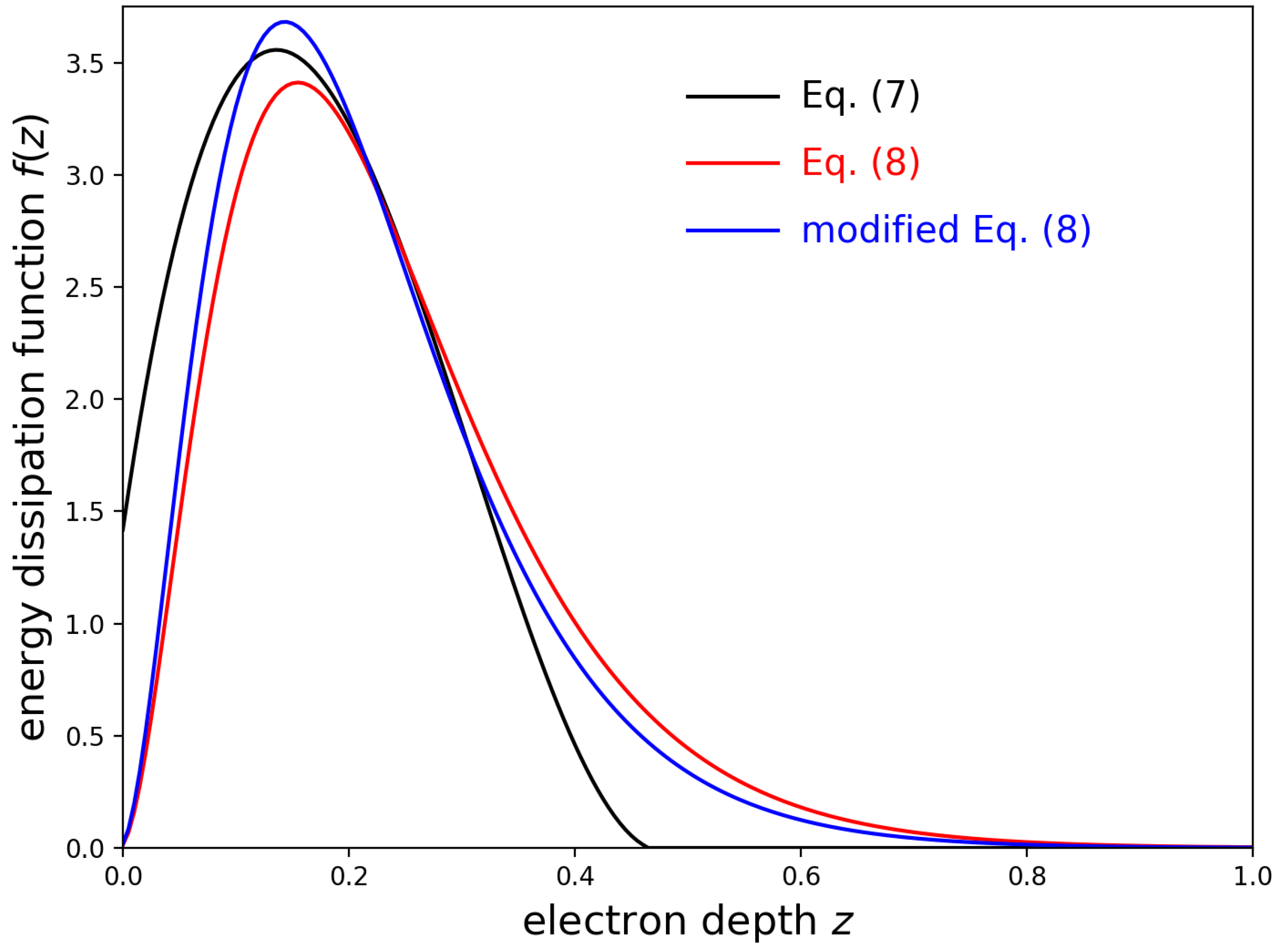
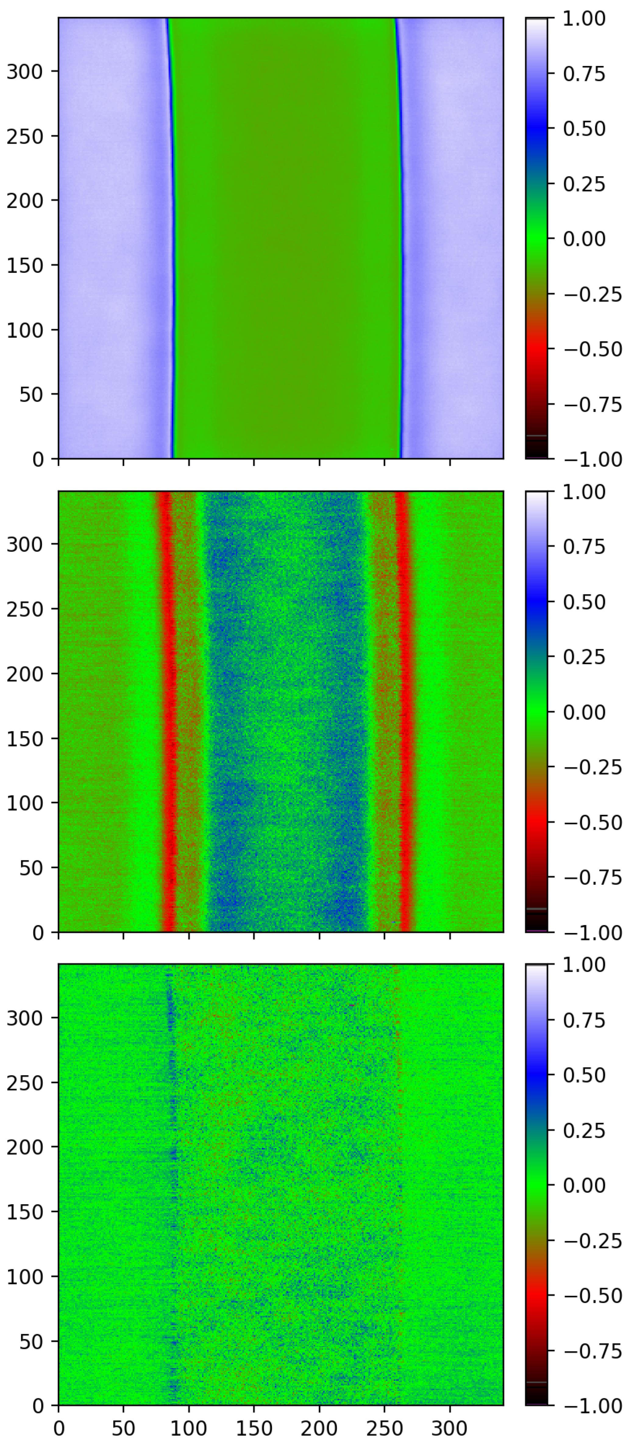
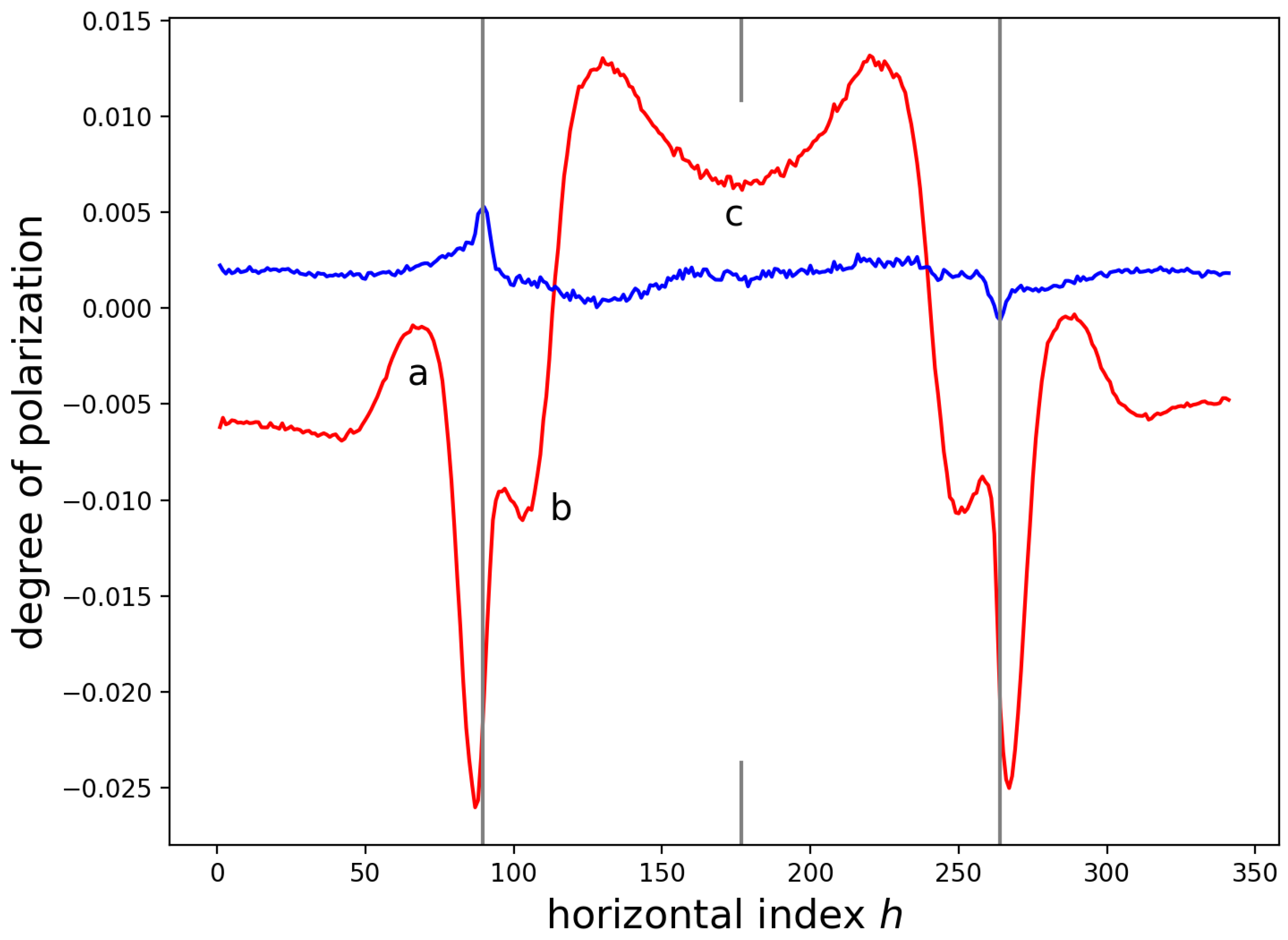
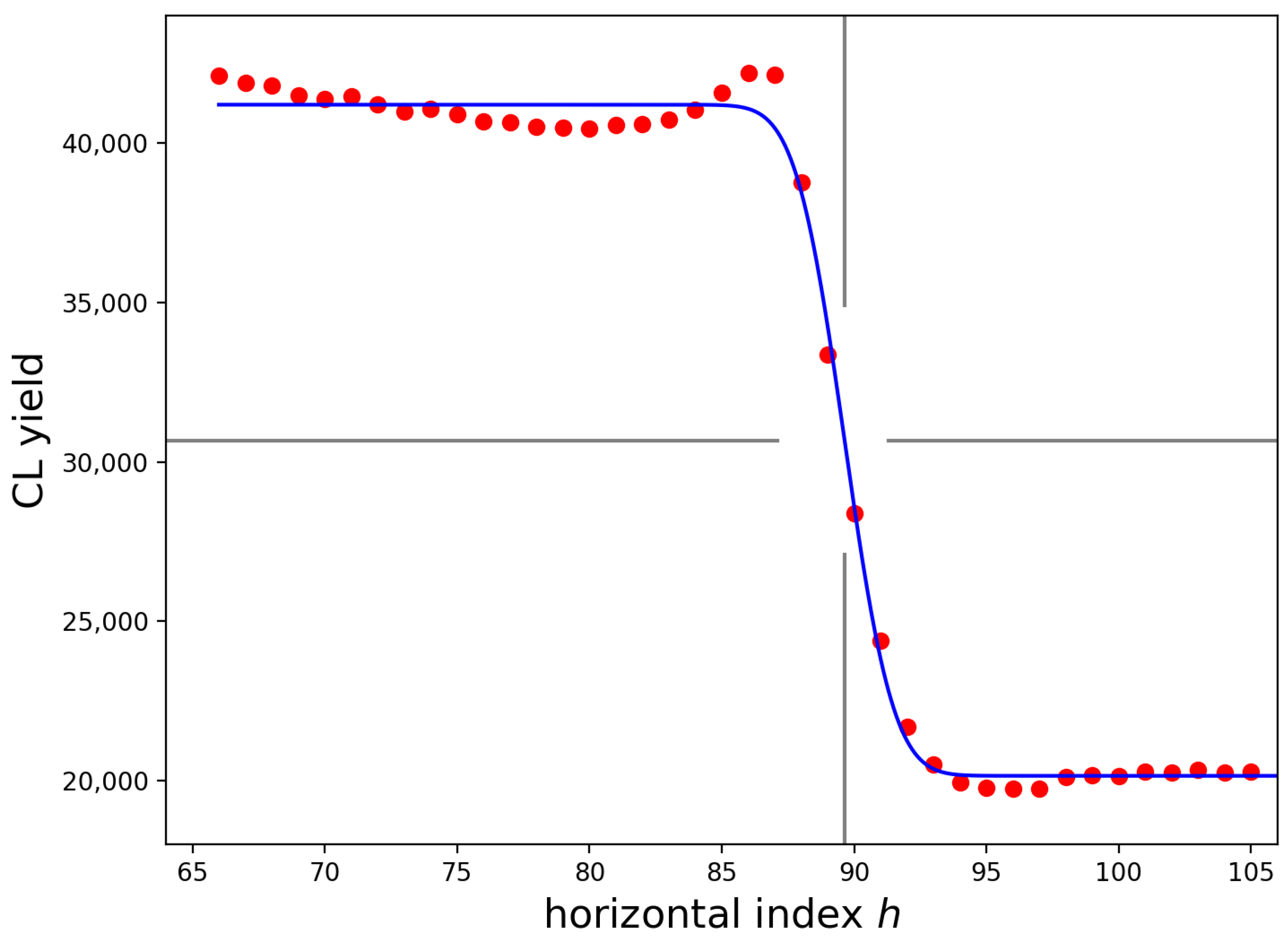
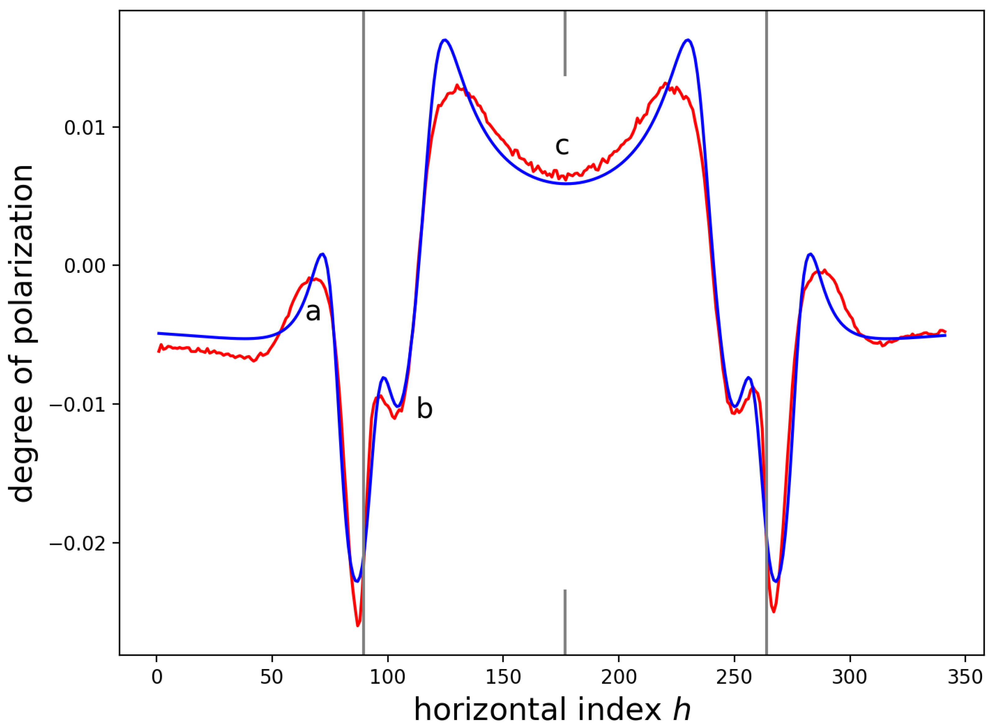
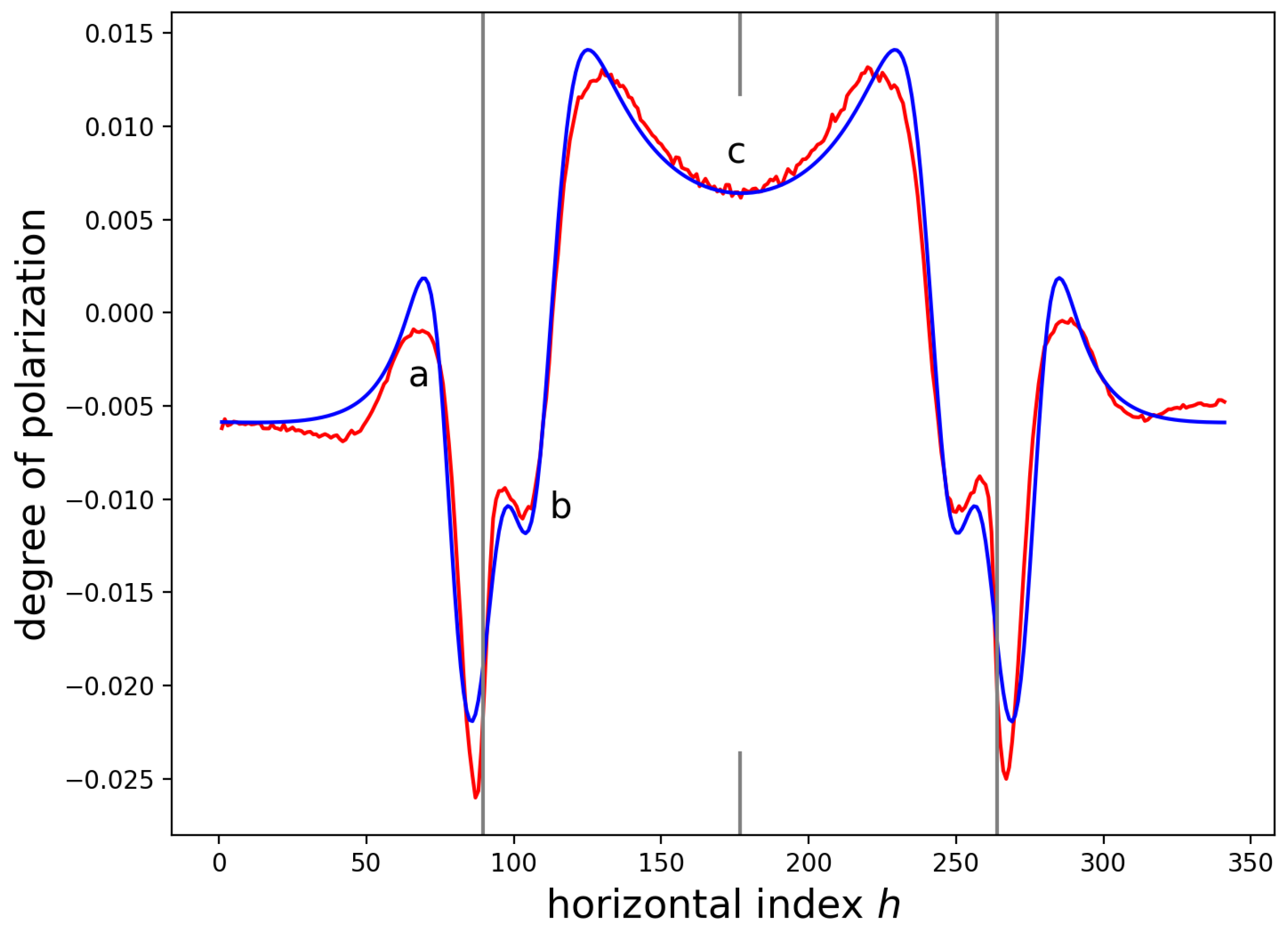
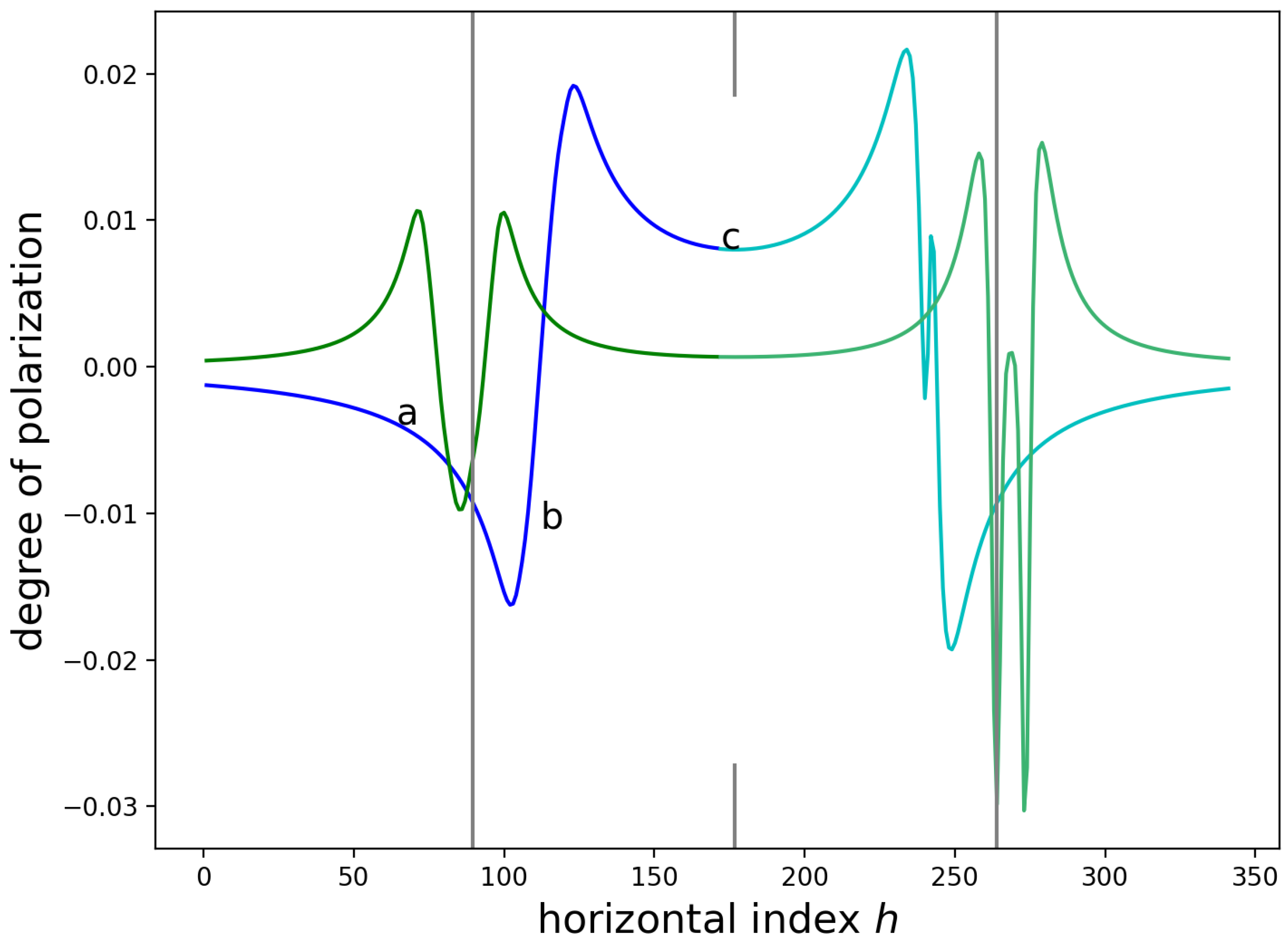
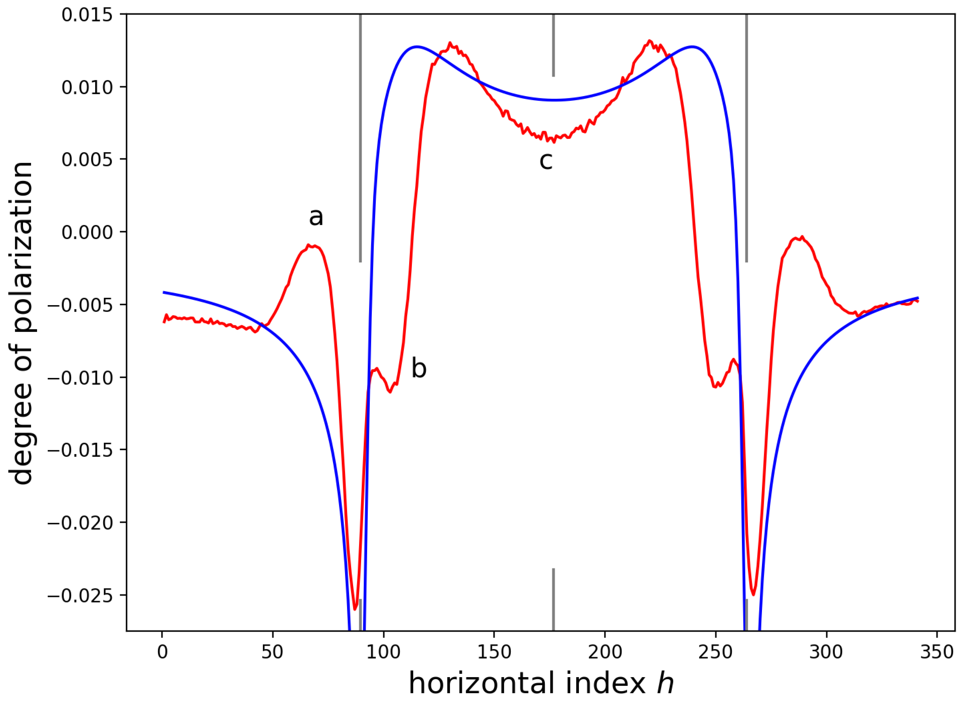
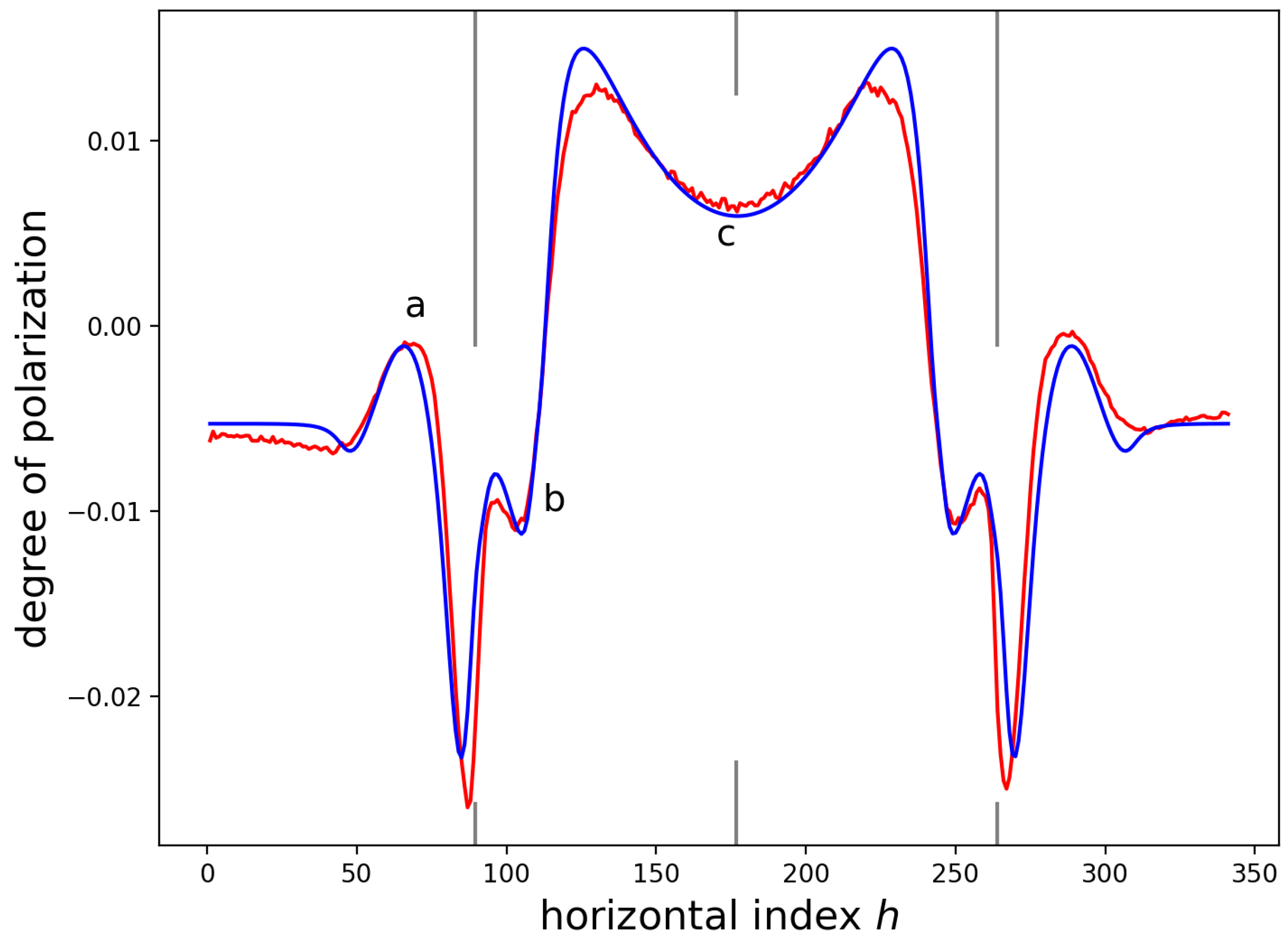
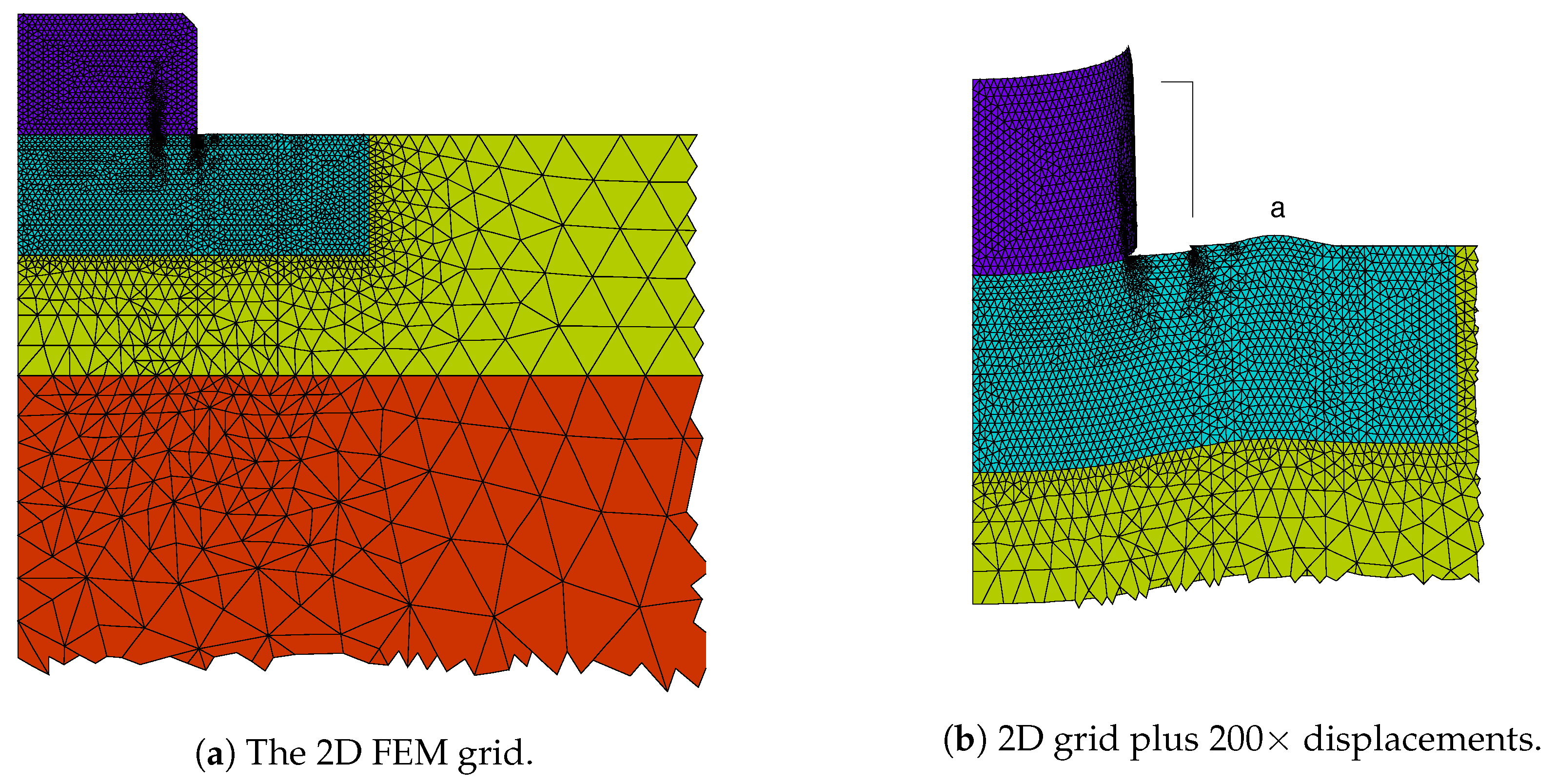
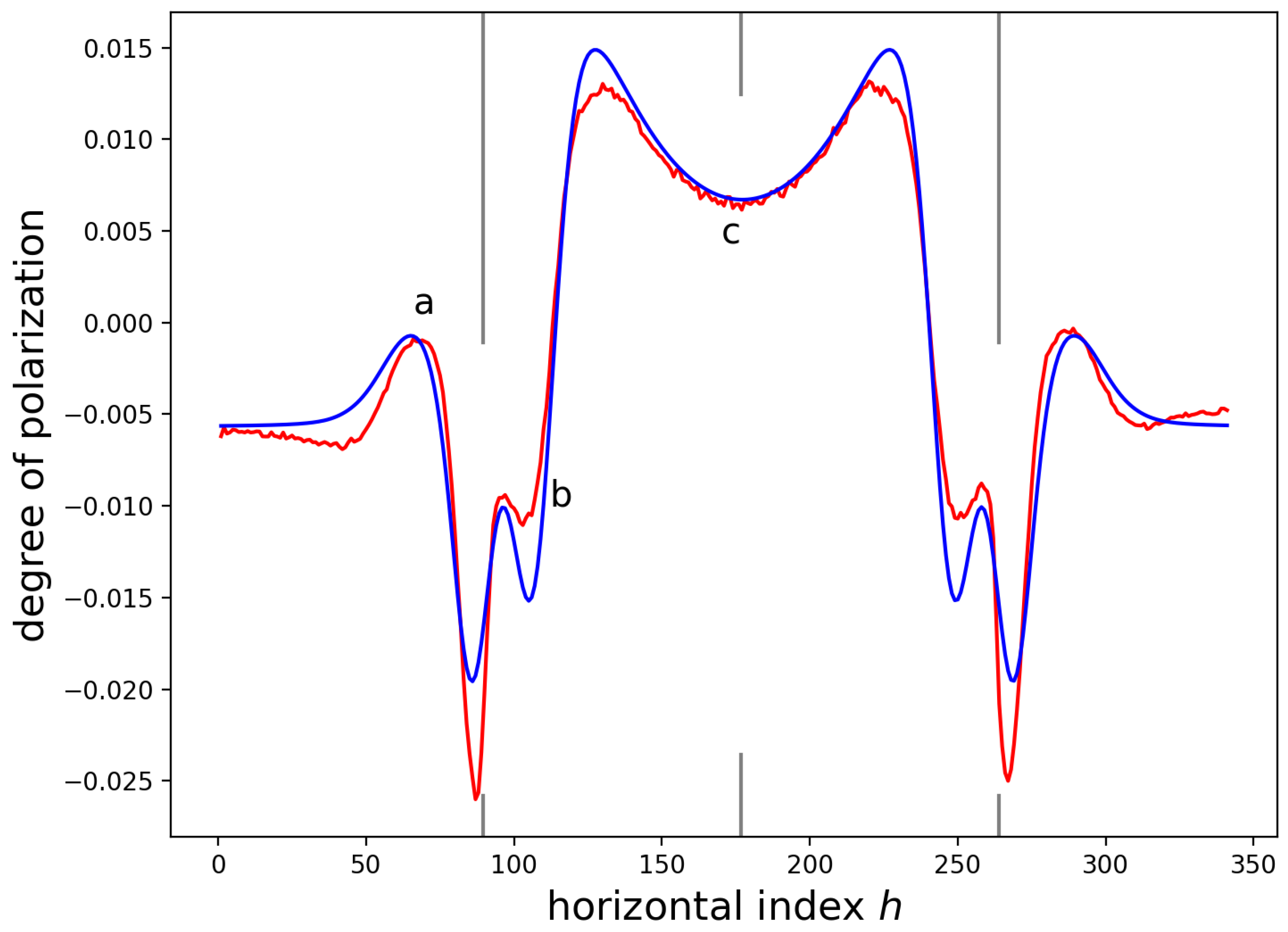
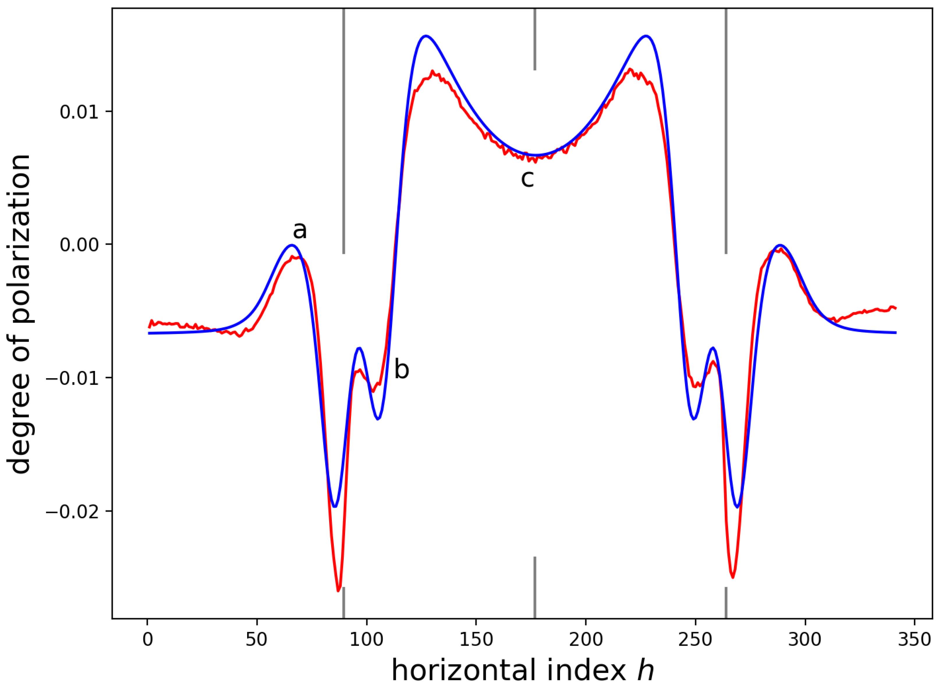
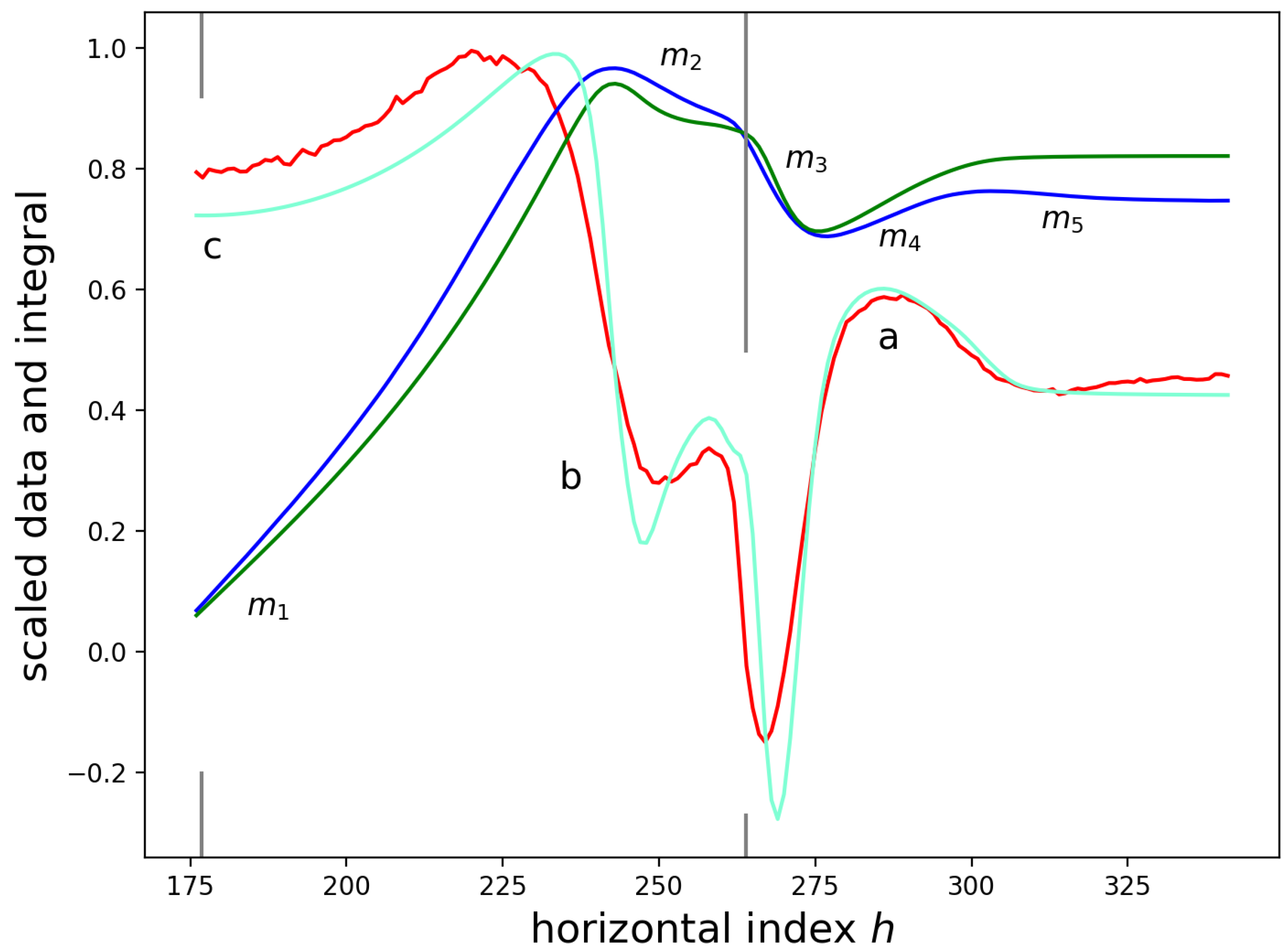
Table 1.
Values for selected points for the three curves of Figure 1.
Table 1.
Values for selected points for the three curves of Figure 1.
| Item | Black | Red | Blue |
|---|---|---|---|
| maximum | |||
| Z | 1 |
Table 2.
Critical values for , assuming values for Al0.4Ga0.6As.
| Label | Area | Notes | ||
|---|---|---|---|---|
| 0 | ||||
| 0.112 | ||||
| 0.223 | ||||
| 0.323 | maximum value of | |||
| 0.423 | ||||
| 0.523 | ||||
| 0.623 | ||||
| 0.723 | ||||
| 0.823 | ||||
| 0.912 | ||||
| 0.990 | ||||
| 1 |
Table 3.
Positions of features in Figure 3, as read from Figure 3 with a crosshair cursor. The midpoint of the width of the SiN stripe is . The estimated positions of the edges of the SiN stripe, SiN left and SiN right, were determined from fits to the CL yield, Section 3.
| Feature | h Index | Diff | Diff (m) |
|---|---|---|---|
| ‘a’ left | 67 | ||
| neg peak | 87 | ||
| ROP left | 89 | ||
| SiN left | 89.65 | ||
| ‘b’ left | 97 | ||
| ‘b’ mid | 100 | ||
| ‘b’ right | 103 | ||
| ‘c’ left | 130 | ||
| ‘c’ mid | 177 | 0 | 0 |
| ‘c’ right | 220 | 43 | 1.53 |
| ‘b’ left | 250 | 73 | 2.60 |
| ‘b’ mid | 255 | 78 | 2.78 |
| ‘b’ right | 258 | 81 | 2.89 |
| SiN right | 263.91 | ||
| ROP right | 265 | 88 | |
| neg peak | 267 | 90 | 3.21 |
| ‘a’ right | 287 | 110 | 3.92 |
Table 4.
Comparison of widths and beam scale parameters for different approaches.
| Approach | Width | (nm) | (nm) | Width (m) | ||
|---|---|---|---|---|---|---|
| corrected | ||||||
| corrected |
Table 5.
Mean rms values for columns of DOP and ROP, and SNR for CL yield.
| Item | GaAs [0:40] | SiN [144:206] | GaAs [:] |
|---|---|---|---|
| 38 | 58 | 28 | |
| mean rms DOP | |||
| mean rms ROP | |||
| SNR CL yield | 120 | 80 | 181 |
Table 6.
Measured and estimated minimum detectable changes in DOP or ROP, , for CL measurements of top (8 keV) and facet (5 keV), and for PL measurements. is the number of data points involved in the calculation of the average DOP or ROP value.
Table 6.
Measured and estimated minimum detectable changes in DOP or ROP, , for CL measurements of top (8 keV) and facet (5 keV), and for PL measurements. is the number of data points involved in the calculation of the average DOP or ROP value.
| Description | Ref. | Notes | ENBW | |||
|---|---|---|---|---|---|---|
| this work | Table 5 | measured | 30 Hz | |||
| this work | Table 5 | 1 | extrapolated | 90 kHz | ||
| facet CL, 5 keV | [41] | 15 | measured | 6 kHz | ||
| facet CL, 5 keV | [41] | 1 | extrapolated | 90 kHz | ||
| facet PL | [22,48] | 1 | measured | 3.33 Hz |
Table 7.
Parameter values for fits of plane strain and plane stress approximations to the measured DOP for two different spatial resolutions.
Table 7.
Parameter values for fits of plane strain and plane stress approximations to the measured DOP for two different spatial resolutions.
| Item | Symbol | Plane Strain | Plane Stress | ||
|---|---|---|---|---|---|
| scale parameter | |||||
| multiplier | 1 | 3 | 1 | 3 | |
| Poisson’s ratio | 0 | 0 | |||
| goodness of fit | 30.11 | 24.83 | 24.13 | 23.49 | |
| width (m) | 2.30 | 2.30 | 2.30 | 2.30 | |
| angle (deg) | 20 | 40 | 106 | 114 | |
| width (nm) | 120 | 150 | 195 | 195 | |
| angle (deg) | 82 | 82 | 131 | 133 | |
| ratio | 0.90 | 0.80 | 1.55 | 1.25 | |
| fit parameters | |||||
Disclaimer/Publisher’s Note: The statements, opinions and data contained in all publications are solely those of the individual author(s) and contributor(s) and not of MDPI and/or the editor(s). MDPI and/or the editor(s) disclaim responsibility for any injury to people or property resulting from any ideas, methods, instructions or products referred to in the content. |
© 2024 by the authors. Licensee MDPI, Basel, Switzerland. This article is an open access article distributed under the terms and conditions of the Creative Commons Attribution (CC BY) license (https://creativecommons.org/licenses/by/4.0/).
Share and Cite
MDPI and ACS Style
Cassidy, D.T.; Pagnod-Rossiaux, P.; Mokhtari, M. Degree of Polarization of Cathodoluminescence from a (100) GaAs Substrate with SiN Stripes. Optics 2024, 5, 11-43. https://0-doi-org.brum.beds.ac.uk/10.3390/opt5010002
AMA Style
Cassidy DT, Pagnod-Rossiaux P, Mokhtari M. Degree of Polarization of Cathodoluminescence from a (100) GaAs Substrate with SiN Stripes. Optics. 2024; 5(1):11-43. https://0-doi-org.brum.beds.ac.uk/10.3390/opt5010002
Chicago/Turabian StyleCassidy, Daniel T., Philippe Pagnod-Rossiaux, and Merwan Mokhtari. 2024. "Degree of Polarization of Cathodoluminescence from a (100) GaAs Substrate with SiN Stripes" Optics 5, no. 1: 11-43. https://0-doi-org.brum.beds.ac.uk/10.3390/opt5010002