
A Single-Voltage-Source Class-D Boost Multi-Level Inverter with Self-Balanced Capacitors


1
Department of Electrical Engineering, Feng Chia University, No. 100, Wenhwa Road, Seatwen, Taichung 40724, Taiwan
2
Department of Electrical Engineering, National Taipei University of Technology, 1, Sec. 3, Zhongxiao E. Rd., Taipei 10608, Taiwan
3
Delta Electronics (Taiwan), No. 16, Dongyuan Rd., Zhongli Dist., Taoyuan City 32063, Taiwan
*
Author to whom correspondence should be addressed.
Energies 2022, 15(11), 4082; https://0-doi-org.brum.beds.ac.uk/10.3390/en15114082
Submission received: 25 April 2022
/
Revised: 30 May 2022
/
Accepted: 31 May 2022
/
Published: 1 June 2022
(This article belongs to the Special Issue Multilevel Converter Topology, Design, and Applications)
Abstract
:A symmetric single-source 7-level DC-AC converter with voltage gain of 3 and self-voltage balance is presented by combining the Class-D amplifier and the diode-clamped DC-AC converter. There is only one switch is switched for any time in this circuit. As a result, the conversion efficiency can be upgraded significantly as well as the control strategy can be simplified considerably. In the paper, the operation principle and circuit design of this converter are analyzed in detail, and its feasibility and effectiveness are verified by simulation and digital control, respectively.
1. Introduction
With the rapid development of technology and power electronics in recent years [1], a large amount of low-frequency harmonic currents, generated by the non-linear loads of power electronics, flow into the power system, resulting in increasingly serious harmonic pollution of the power system. As the generated harmonic is larger or exceeds the tolerance value, it may cause other nearby non-linear load products to mis-activate, mis-measure, degrade efficiency or even burn out. The International Electrotechnical Commission (IEC) in Europe has issued IEC 61000-3-2 Harmonic Specification [2], and the Japanese Specifications have also issued JIS-C-61000-3-2 standard [3] has been promulgated by the Japanese Specifications to formally regulate the harmonics generated by electronic devices.
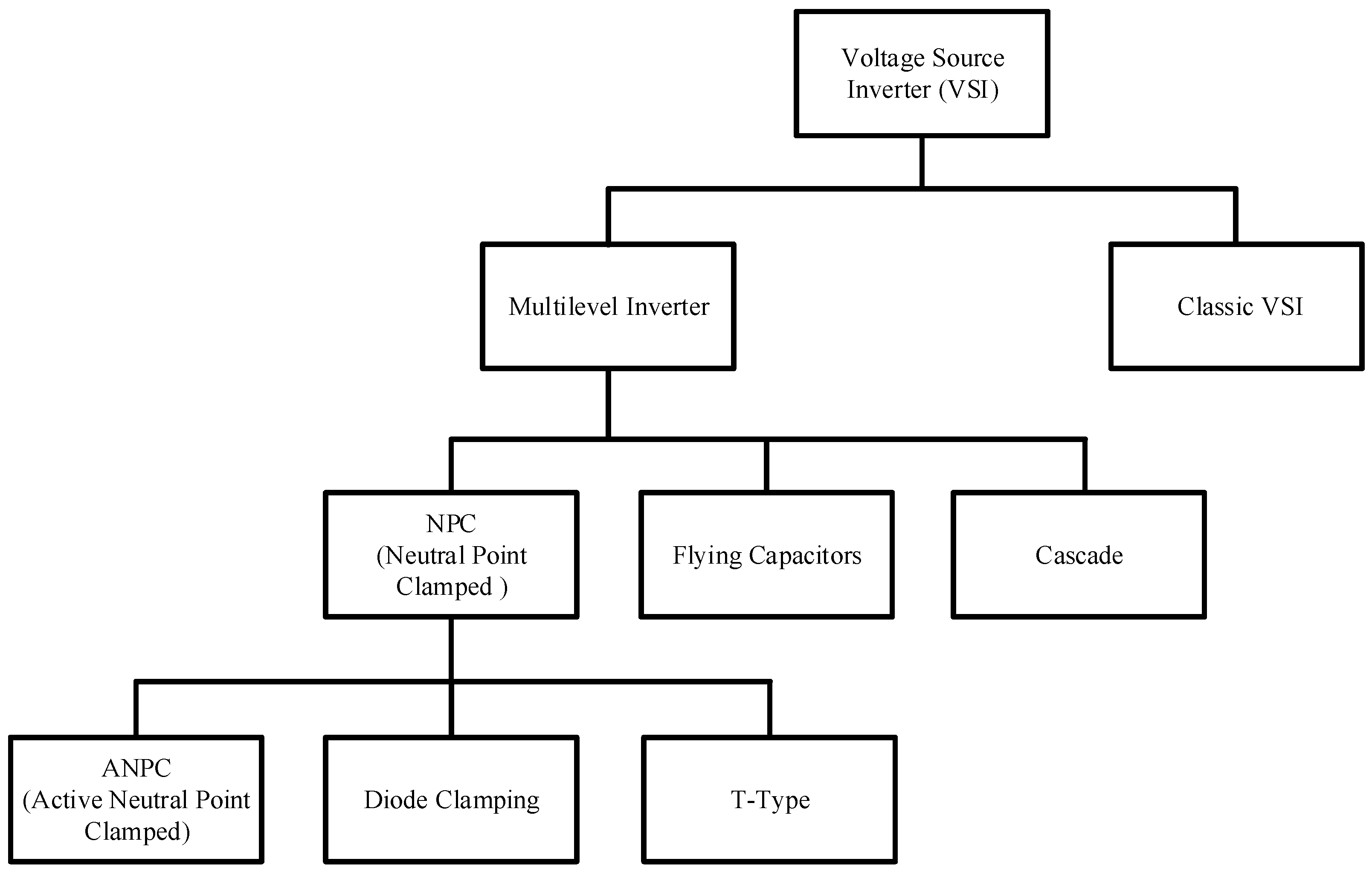
In order to cope with the AC systems used in the market, DC-AC converters or AC-DC converters combined with DC-AC converters are used to convert the green energy to AC power. Therefore, DC-AC converters are one of the most important technologies used in the industry today. Multi-level DC-AC converters use switching paths to make the output voltage appear in a hierarchical pattern and increase the number of levels or filters to make the output voltage appear like a sine wave. The output voltage of the multistage DC-AC converter is in the form of a stratified output voltage so that the voltage stress on the switch can be clamped. Therefore, the high-voltage AC output can be achieved with the switch with the low-voltage stress. Figure 1 shows the generalized classification of voltage-type multi-stage DC-AC converters, which contain neutral point clamped converters [4], the flywheel capacitor type [5] and the series-connected type [5].
Flying capacitors are DC-AC converters that use multiple capacitors connected to each other to achieve output voltage clamping. However, a large number of capacitors and complex control methods are required to balance the capacitor voltage to achieve a hierarchical output voltage [5].
Although the cascade structure has the characteristics of modular design and floating power supply, it requires multiple independent power inputs to achieve a hierarchical AC output voltage [5].
The circuit structure presented in [4] uses diodes and switches to create a neutral potential for the output voltage, which has a lower harmonic content than the conventional two-level DC-AC converter. The pulse width modulation (PWM) method proposed in [6] is based on the comparison of sine and triangle waves to generate suitable driving signals to turn on/off switches, which in turn make the output voltage appear in the form of a sine wave.
Studies referenced in [7,8] propose a neutral point clamping circuit. The circuit structure presented in [7] consists of six switches and a floating capacitor to realize a DC-AC converter with a voltage gain of 1 at 5 levels. The circuit structure presented in [8] is similar to that of [7] and adopts nine switches to realize a DC-AC converter with a voltage gain of 1.5 at 7 levels. By adding two additional switches and one floating capacitor, a DC-AC converter with a voltage gain of 1 at 9 levels can be realized with eleven switches, two DC link capacitors, and two floating capacitors. At the same time, with the same number of components, a DC-AC converter with a voltage gain of 2.5 at 11 levels can be realized by only changing the switching sequence. The literature [9] proposes a circuit that can operate in a reactive power condition by combining the concept of diode clamping, flywheel capacitor, and T-type active clamping to design a DC-AC converter with a voltage gain of 0.5 at 5 levels.
In [10], a step-up converter is used to provide the required step voltage for the H-bridge output. This approach not only achieves the purpose of the DC step-up voltage but also uses the inductor of this circuit as the input inductor to reduce the input current ripple. In addition, in [10], a 5-, 7-, and 15-level circuit structure is proposed to realize the high-level AC output and applied to the fuel cell system. In [11,12], floating capacitors are used to increase the number of levels of the DC-AC converter. This circuit structure can be used to increase the voltage gain with a single power input, but the floating capacitor must be self-balanced to output the step voltage. The structure proposed in [11] uses two floating capacitors and two diodes along with the required switching sequence to achieve self-balancing of the capacitors, resulting in a voltage gain of 2 at nine levels. In [12], a circuit with three floating capacitors and three diodes is presented, and the capacitor voltage is one to two times the input voltage, so the number of output levels can reach nine with a voltage gain of 4. However, this method will increase the voltage stress on the switch, so a higher specification switch is required. In [13], a modified pulse width modulation control method is proposed to combine the active clamping circuit with the H-bridge structure so that the capacitor voltage across the H-bridge can maintain self-balance in each level.
Therefore, based on the Class-D amplifier and the traditional diode clamped DC-AC converter, a single-voltage-source symmetric two-output-port 7-level DC-AC converter along with only one switch is switched for any time in this circuit is presented. As a result, not only the proposed converter can possess a 3-voltage-gain and the adopted capacitors with the inherent capability of self-voltage balance, but also the conversion efficiency can be upgraded significantly as well as the control strategy can be simplified greatly. In addition, due to the symmetric structure, the interchangeability of mass production of this converter can be easily realized. In the paper, the feasibility of the proposed circuit is demonstrated by simulating a 300 W prototype circuit, and the effectiveness of this prototype circuit is confirmed by using a single comparator PWM voltage feedback control [14] based on the field programmable gate array (FPGA).
2. Operating Principles of the Proposed Circuit
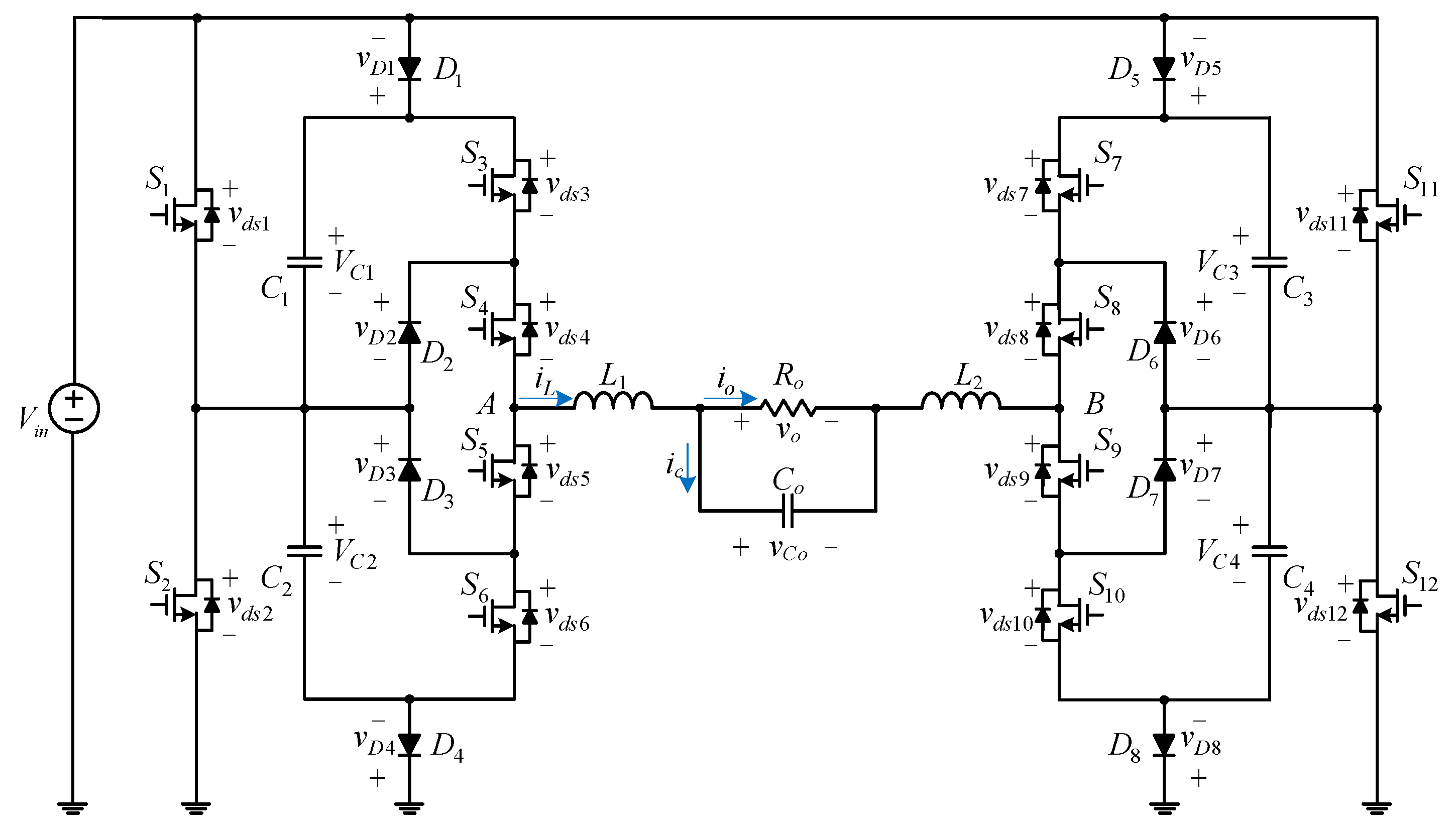
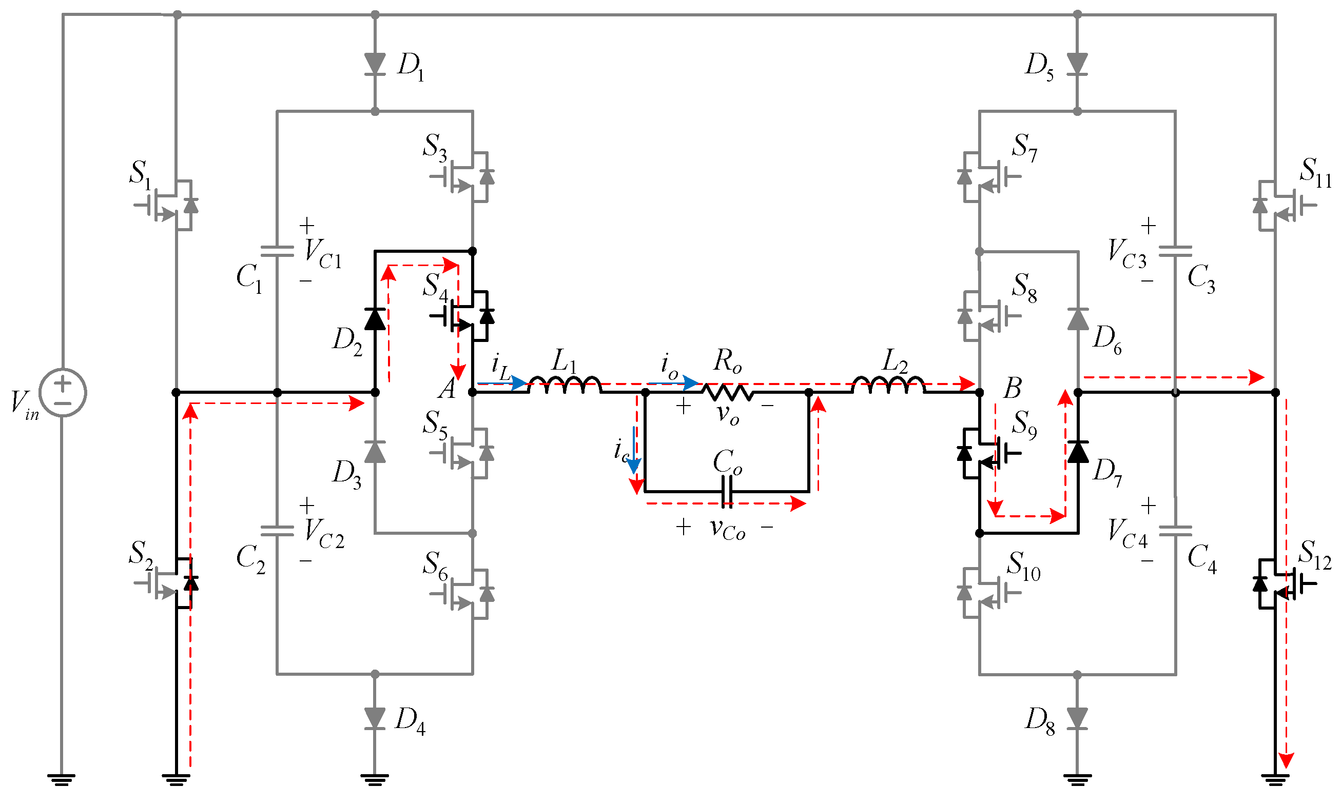
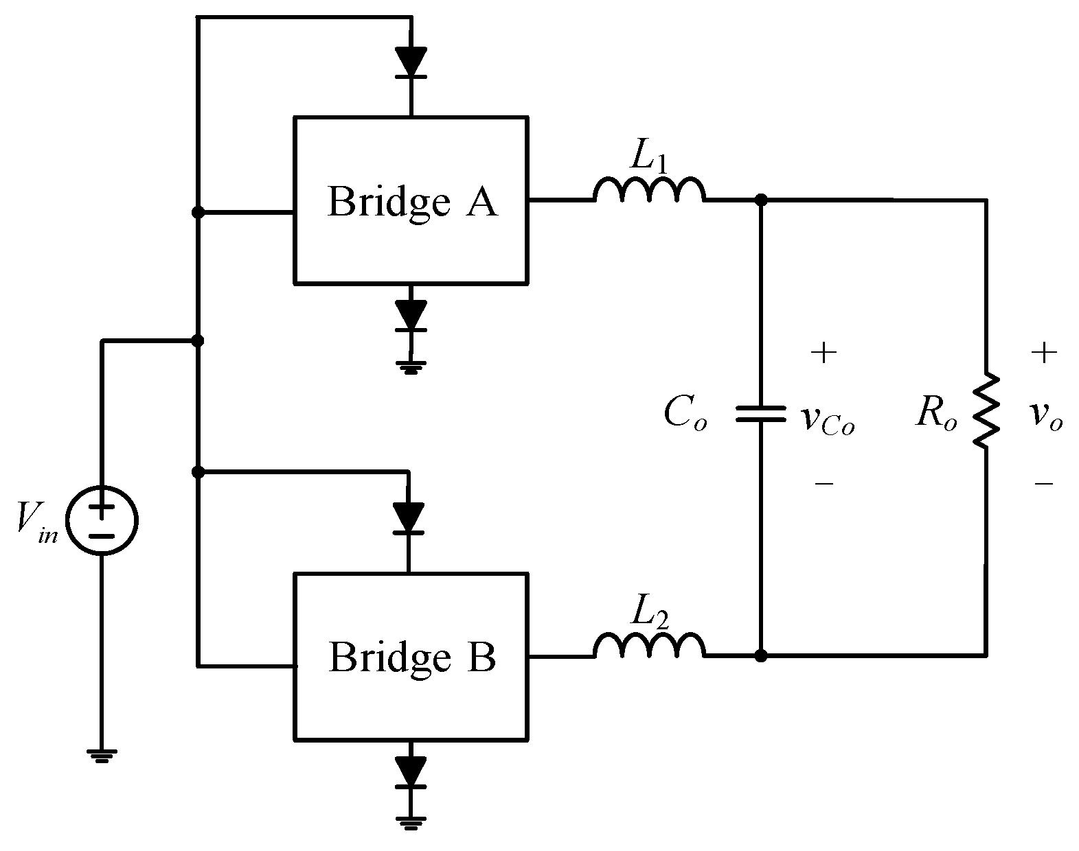
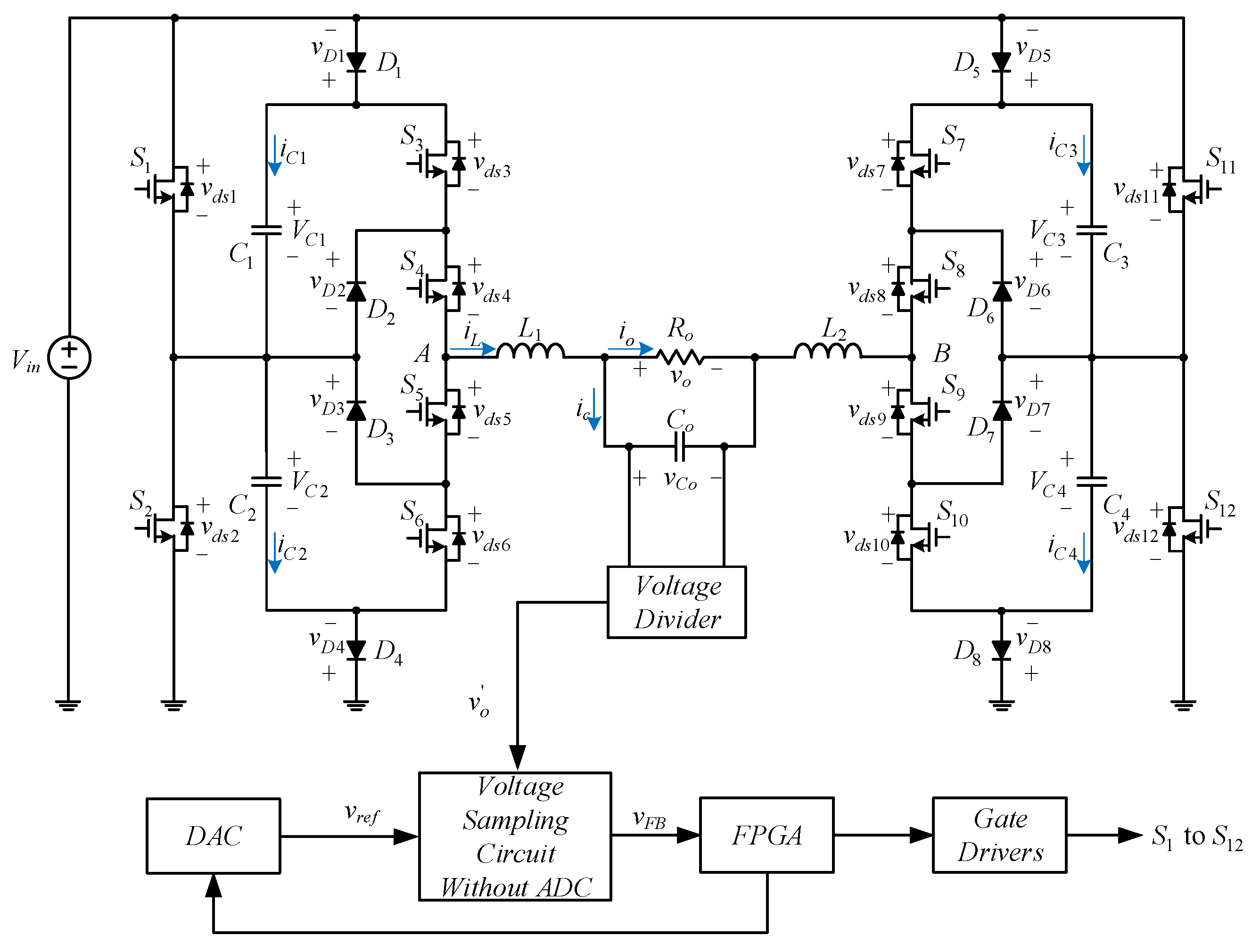
Figure 2 shows the proposed single-voltage-source class-D 7-level DC-AC converter. This converter is composed of 12 switches, 8 diodes, and 4 energy-transferring capacitors.
Before the operating analysis, a brief description of the relevant symbol definitions and required assumptions is given: (1) Vin is the input voltage, vo is the output voltage, and the voltage vCo of the filter capacitor Co is equal to vo; (2) S1 to S12 are the switches with the corresponding cross-voltages vds1 to vds12; (3) D1 to D8 are diodes with the corresponding cross-voltages, vD1 to vD8; (4) C1 to C4 are energy-transferring capacitors with the corresponding currents iC1 to iC4; (5) the values of the energy-transferring capacitors are assumed to be large enough that the voltages across them can be considered constant, i.e., VC1 = VC2 = VC3 = VC4; (6) io is the output current; (7) iL is the current flowing through inductors L1 and L2; and (8) all components are regarded as idea except for the body diodes of the switches.
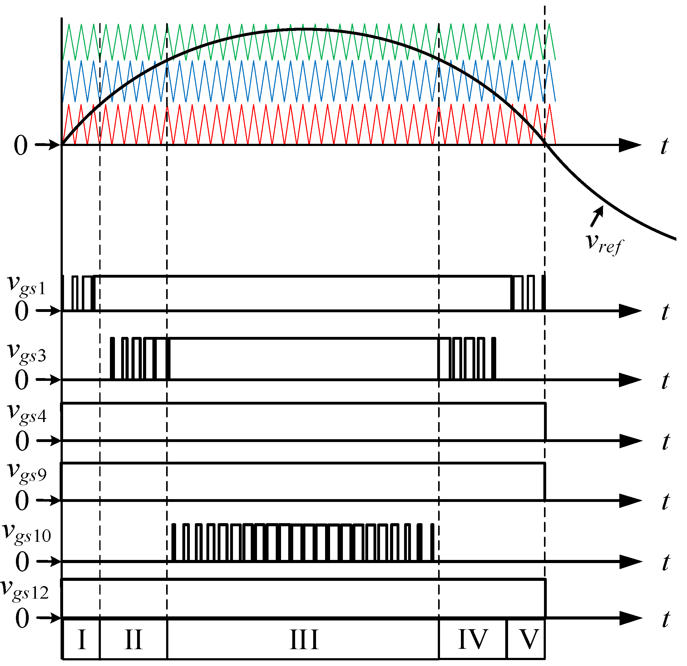
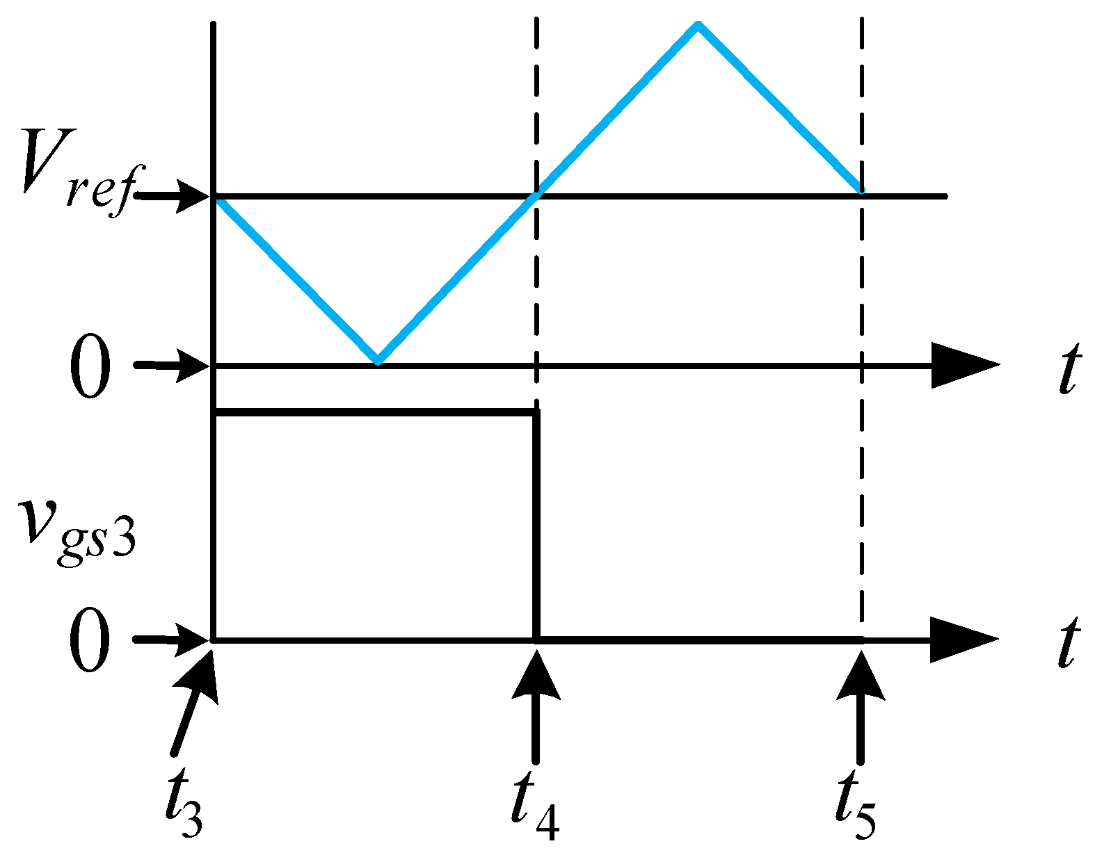
Figure 3 shows the waveforms of the gate driving signals for switches. Since the gate driving signals are the same at the positive and negative half cycles, only the positive half-cycle is analyzed. The circuit operation behavior has five stages, only one switch will be in PWM switching in each stage, and the other switches are normally on or normally off. Since stage I is equivalent to stage V and stage II is equivalent to stage IV, only stages I, II, and III are analyzed.
When the output voltage is at the positive half cycle, the switches S4, S9, and S12 remain on, and the switches S2, S5, S6, S7, S8, and S11 remain off. The output voltage can be determined by switching S1, S3, and S10 to determine the circuit operation behavior of stages I, II, and III, respectively. Note that in the following descriptions, only one switch is switched at any time, and the current path is marked to show that the converter satisfies energy conservation and Kirchhoff’s voltage and current laws in any stage.
2.1. Stage I
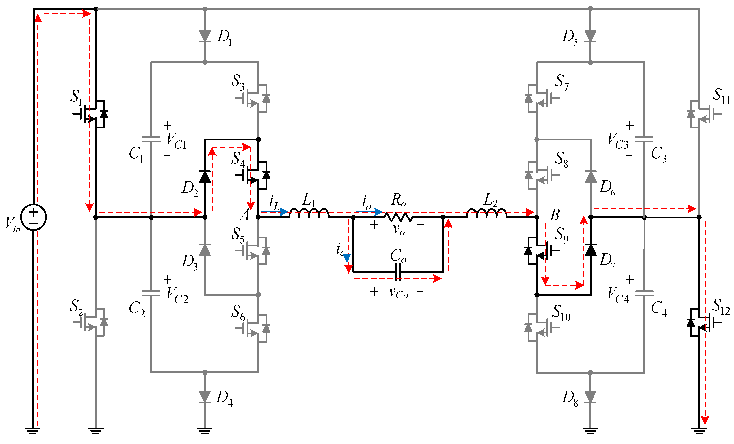
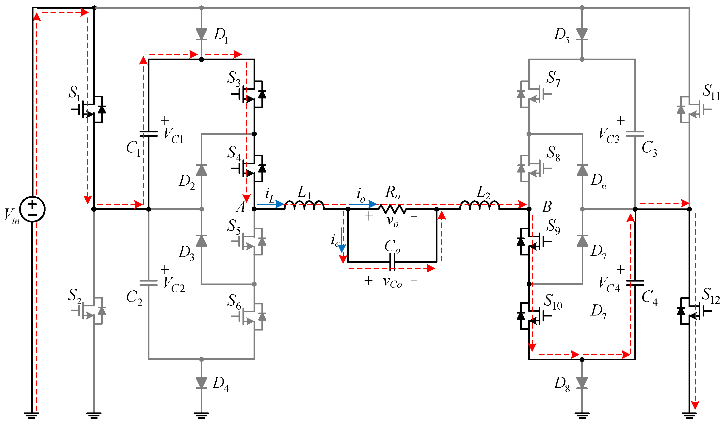
Only the switch S1 is switched as in Figure 4.
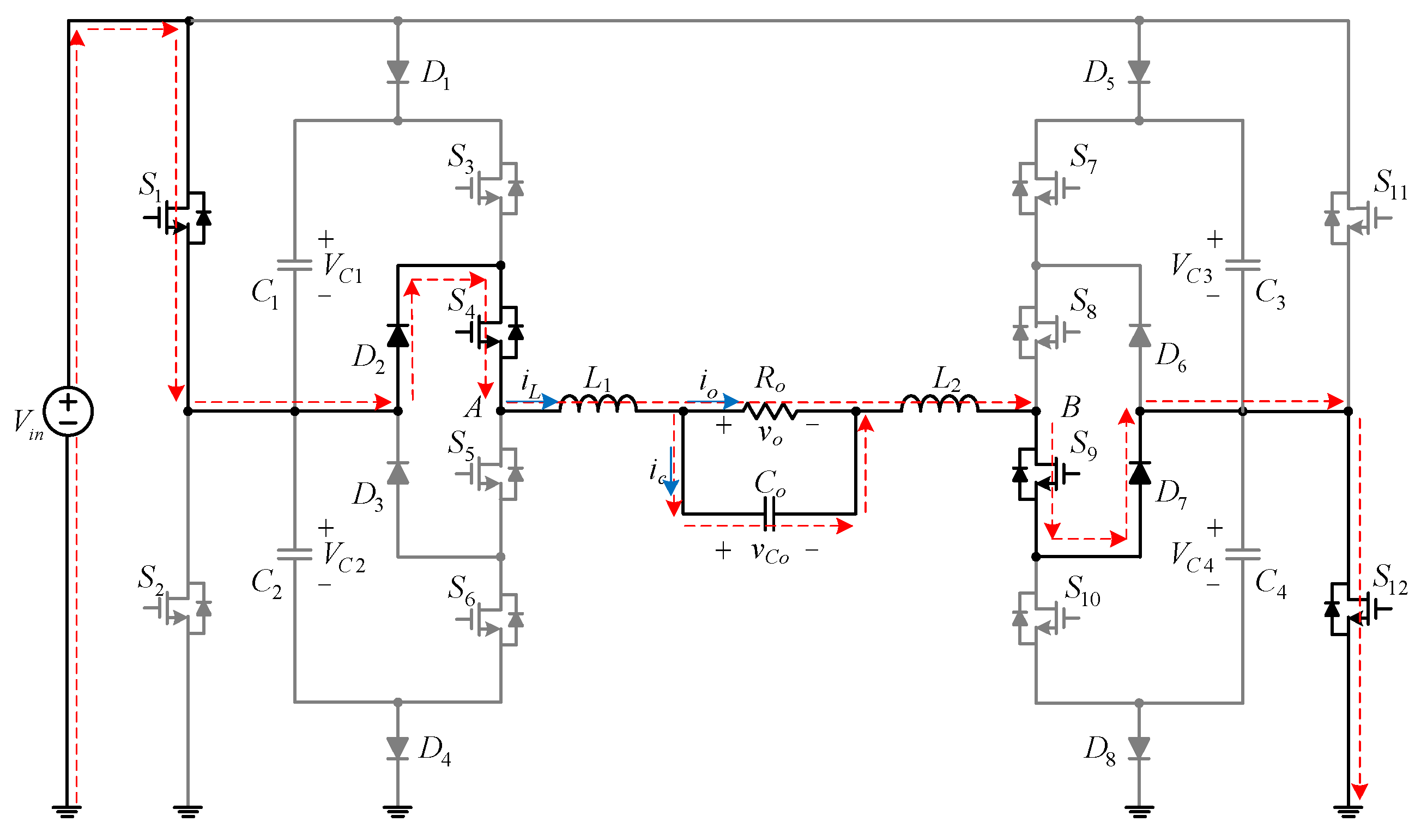
Interval : The switch S1 is on, but the switches S3 and S10 are off. As shown in Figure 5, the current flowing through the inductors L1 and L2 will form a circuit loop from the input voltage to the switches S1, S4, S9, S12 and the diodes D2, D7; therefore, the voltage across the terminals A and B is
Interval : The switches S1, S3 and S10 are all off. At the same time, the input voltage is disconnected from the output. As shown in Figure 6, the current flowing through the inductors L1 and L2 will form a circuit loop from the switches S4, S9, S12 to the diodes D2, D7 and the body diode of the switch S2, so the voltage across the terminals A and B is
2.2. Stage II
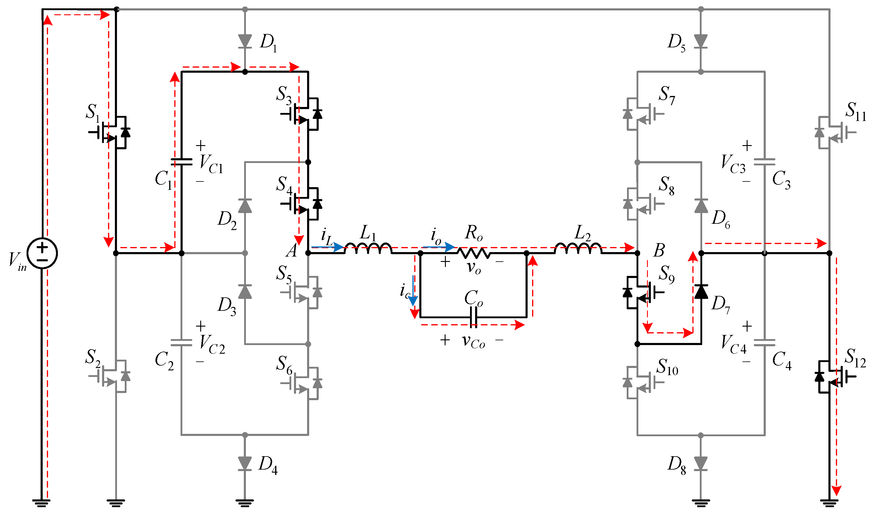
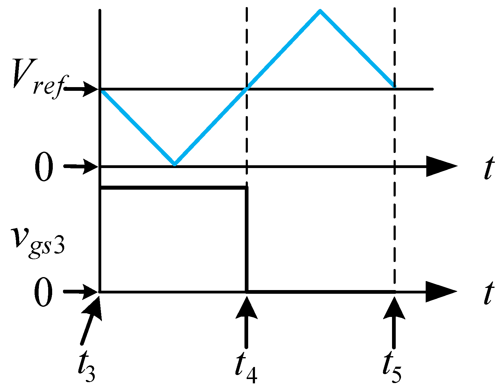
Only the switch S3 is switched as in Figure 7.
Interval : The switches S1 and S3 are on, but the switch S4 is off. As shown in Figure 8, the current flowing through the inductors L1 and L2 will form a circuit loop from the input voltage to S1, S3, S4, S9, S12 and the diode D7; therefore, the voltage across the terminals A and B is
Interval : The switches S3 and S10 are off, but the switch S1 is on. As shown in Figure 9, the current flowing through the inductors L1 and L2 will form a circuit loop from the input voltage to the switches S1, S4, S9, S12 and the diodes D2, D7; therefore, the voltage across the terminals A and B is
2.3. Stage III
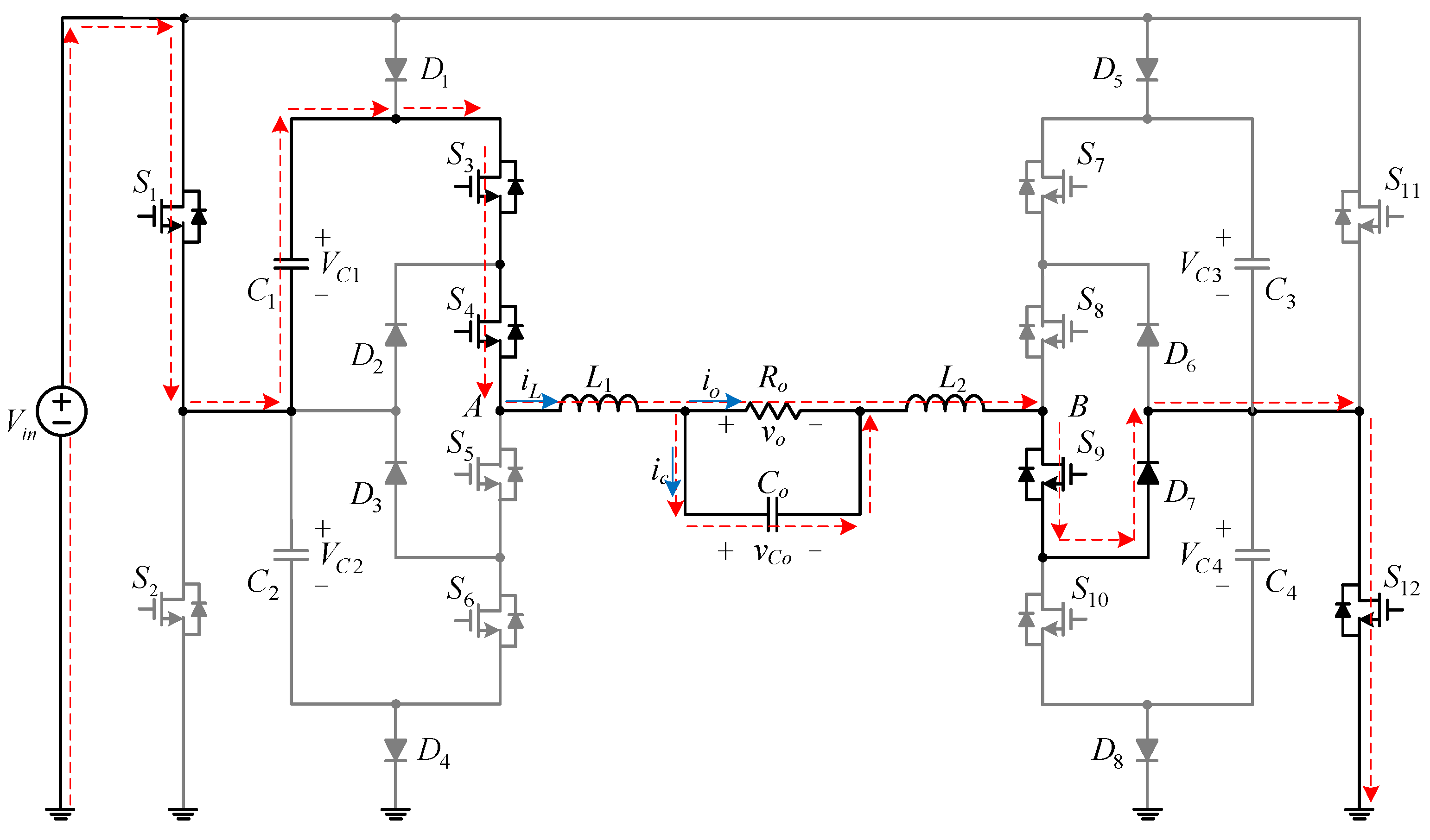
Only the switch S10 is switched as in Figure 10.
Interval : The switches S1, S3 and S10 are turned on. As shown in Figure 11, the current flowing through the inductors L1 and L2 will form a circuit loop from the input voltage to the switches S1, S3, S4, S9, S10 and S12; therefore, the voltage across the terminals A and B is
Interval : The switch S10 is off, but the switches S1 and S3 are on. As shown in Figure 12, the current flowing through the inductors L1 and L2 will form a circuit loop from the input voltage to the switches S1, S3, S4, S9, S12 and the diode D7; therefore, the voltage across the terminals A and B is
From the above analysis, we can see that the proposed 7-level DC-AC converter has the voltage gain of 3, which can be obtained based on (7):
Table 1 shows the switching behavior of the proposed single voltage source Class-D 7-level DC-AC converter and its corresponding maximum voltage stress, where fPWM is the switching frequency and fline is the output voltage frequency or mains frequency. For the output voltage at positive half cycle to be considered, the switches S2, S5, S6, S7, S8 and S11 are off, their maximum voltage stress is Vin. In addition, all the diodes have the maximum voltage stress of Vin.
Table 1 shows the switching behavior of the proposed single voltage source Class-D 7-level DC-AC converter and its corresponding maximum voltage stress. In addition, the switches S1, S3 and S10 take important roles in stages I, II and III.
3. Design Considerations
The specifications of the proposed 7-level DC-AC converter are shown in Table 2.
3.1. Design of Energy-Transferring Capacitors
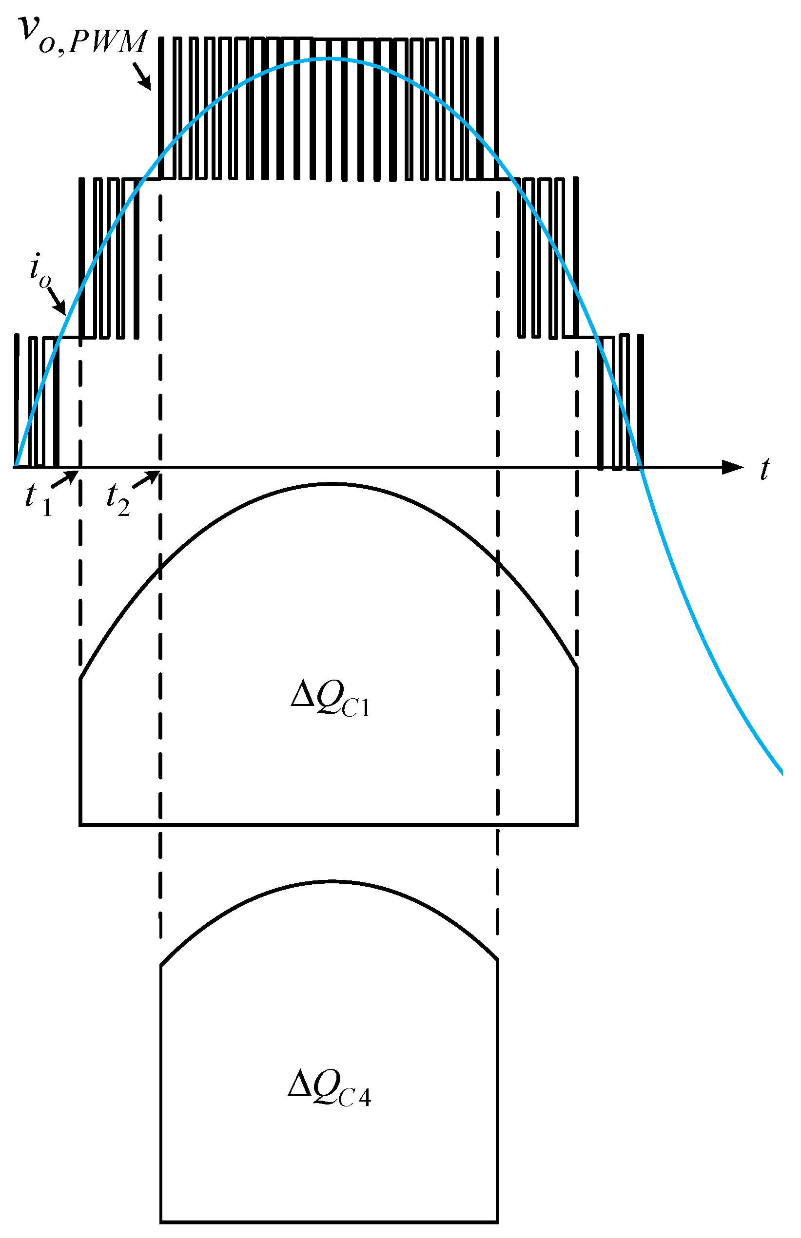
The energy-transferring capacitors used in the proposed converter can be divided into two types according to the discharge time. The first one is the capacitor C1 (=C3) which provides the AC output of stage II and stage III, whereas the second one is the capacitor C4 (=C2) which provides the AC output of stage III. Therefore, based on the concept from Figure 13 and by using Equations (8) and (9), the charge discharged from C1 and C4 over one cycle of the mains power can be calculated:
According to (10), the voltage variation is proportional to the charge variation. Since the results of (8) and (9) can be obtained by PSIM simulation, the value of the capacitor can be worked out under a given voltage ripple percentage of 10% as below:
Therefore, a 3.3 mF electrolytic capacitor is used for each capacitor, which has the voltage across it is equal to the input voltage. Since the derating of the electrolytic capacitor should be taken into considered, the voltage rating of the selected capacitor should be at least 1.25 times the input voltage, according to the usual thumb rule. Finally, a 3300 μF/100 V Rubycon electrolytic capacitor is chosen as each capacitor.
3.2. Design of the Filter
According to the harmonic voltage limit value proposed by IEEE 519-1992, the total harmonic distortion rate is up to 5% below 69 kV [15]. The proposed structure is a 7-level DC-AC converter with a double-ended symmetrical output, which has a filter shown in Figure 14. As generally known, the inductance has higher reactance for high frequency signals, whereas the capacitance has lower reactance for high frequency signals. Therefore, dividing the inductance of LC filter into L1 and L2 not only makes the differential-mode noise filtered by inductance and capacitance and not appear on the output load Ro, but also prevents the common-mode noise from affecting the circuit. Since the switching frequency fs is 60 kHz, the corner frequency fc is set at 6 kHz.
The transfer function of the filter is shown in Equation (14), where :
In (14), we can find
and
Therefore, since fc is 6 kHz, one relationship between L and Co can be obtained based on (15):
Additionally, by rearranging (16), the following equation can be obtained to be
Let the quality factor at rated load be 3 dB, that is, , and the output resistance Ro at rated load is 39.24 Ω. By substituting these values into (18), the other relationship between L and Co can be obtained to be
Substituting (19) into (17) yields
By substituting (20) into (19), the output capacitance can be obtained to be
Finally, a 1 μF/275 V metal film capacitor is chosen as filter capacitor. The actual measured capacitance of 1.02 μF, which is brought into (17) to obtain the filter inductance of 690 μH. Since the filter inductor L is composed of two inductors L1 and L2 connected in series, the values of L1 and L2 are the same, equal to 345 μH.
4. System Block Diagram
Figure 15 shows the system block diagram of the proposed DC-AC converter. The system consists of the main circuit and feedback control circuit. The FPGA digital control core and digital-to-analog converter (DAC) are used to generate a sine wave used as voltage reference, and the ADC-free sampling circuit [14] sends the feedback signal vFB to the FPGA to obtain the corresponding control force after calculation. This control force is then fed to the isolated gate driver to regulate the switch to achieve a stable output voltage.
5. Simulated and Experimental Results along with Discussions
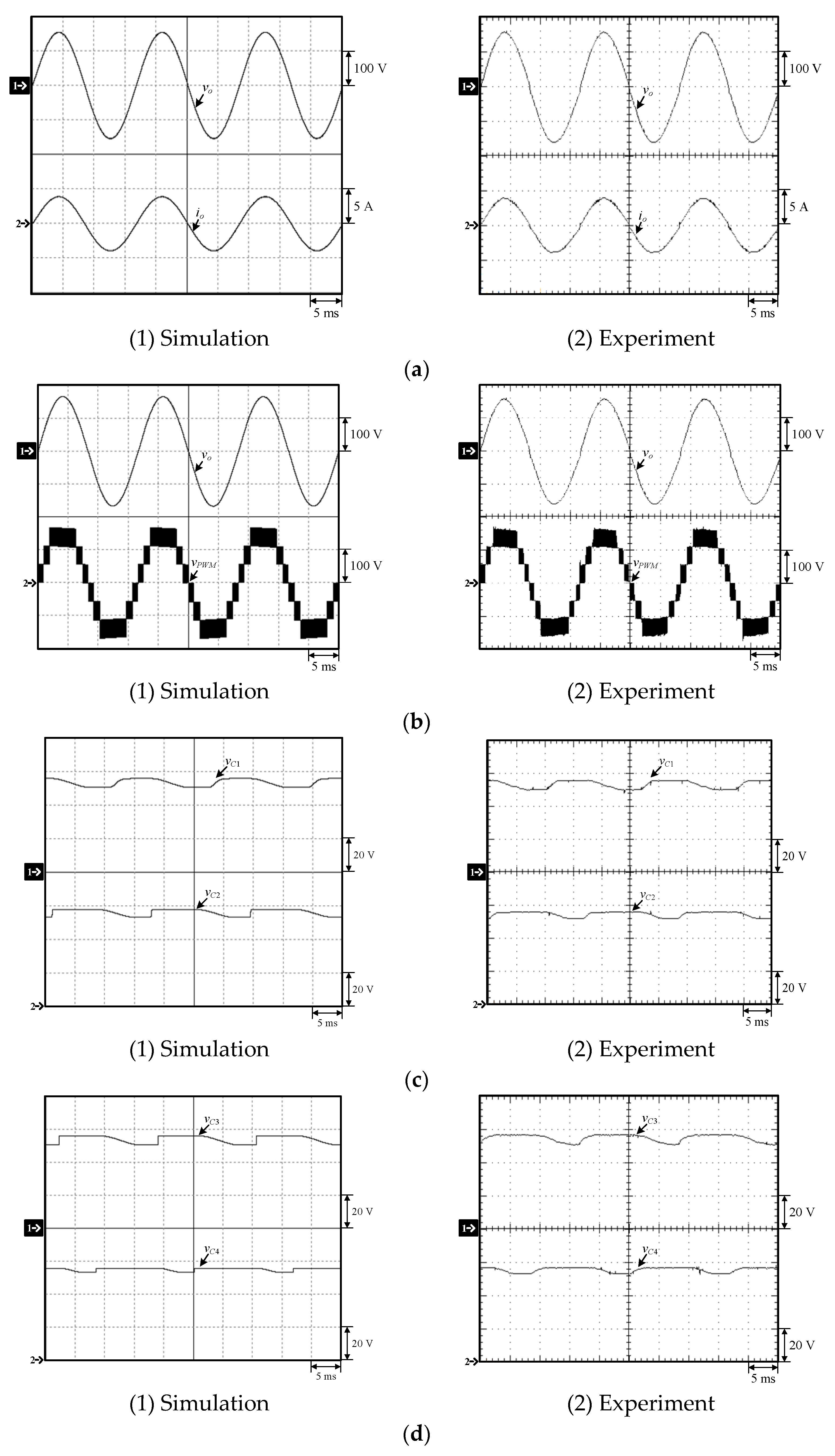
Figure 16 shows the simulated and experimental waveforms of the proposed 7-level DC-AC converter at rated load, containing the output voltage vo and output current io, the unfiltered output voltage vPWM, and the voltages across C1, C2, C3 and C4, called VC1, VC2, VC3 and VC4. From Figure 16a, it can be seen that the output voltage vo and output current io are AC output. From Figure 16b, it can be seen that the unfiltered output voltage vPWM, formed by the high-frequency gate driving signals to turn on and off the switches, is filtered to obtain 60 Hz AC voltage. From Figure 16c,d, it can be seen that all the energy-transferring capacitors in the circuit have the characteristics of self-voltage balance. From the above simulated and experimental results, it can be seen that the proposed 7-level DC-AC converter structure is indeed feasible.
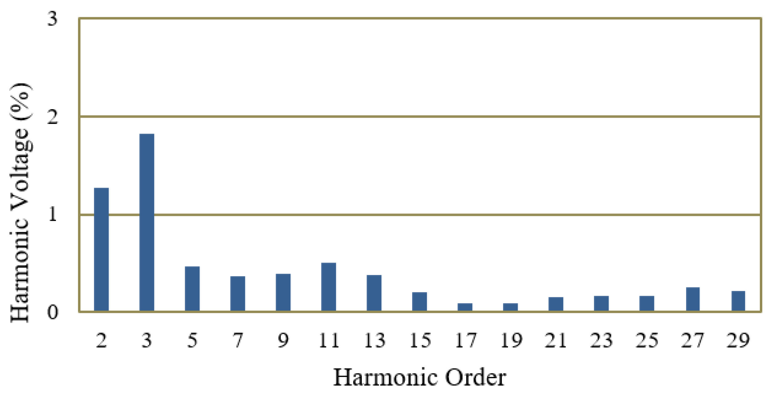
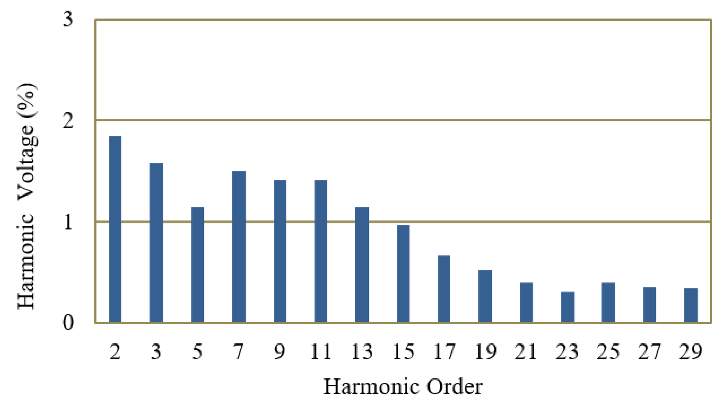
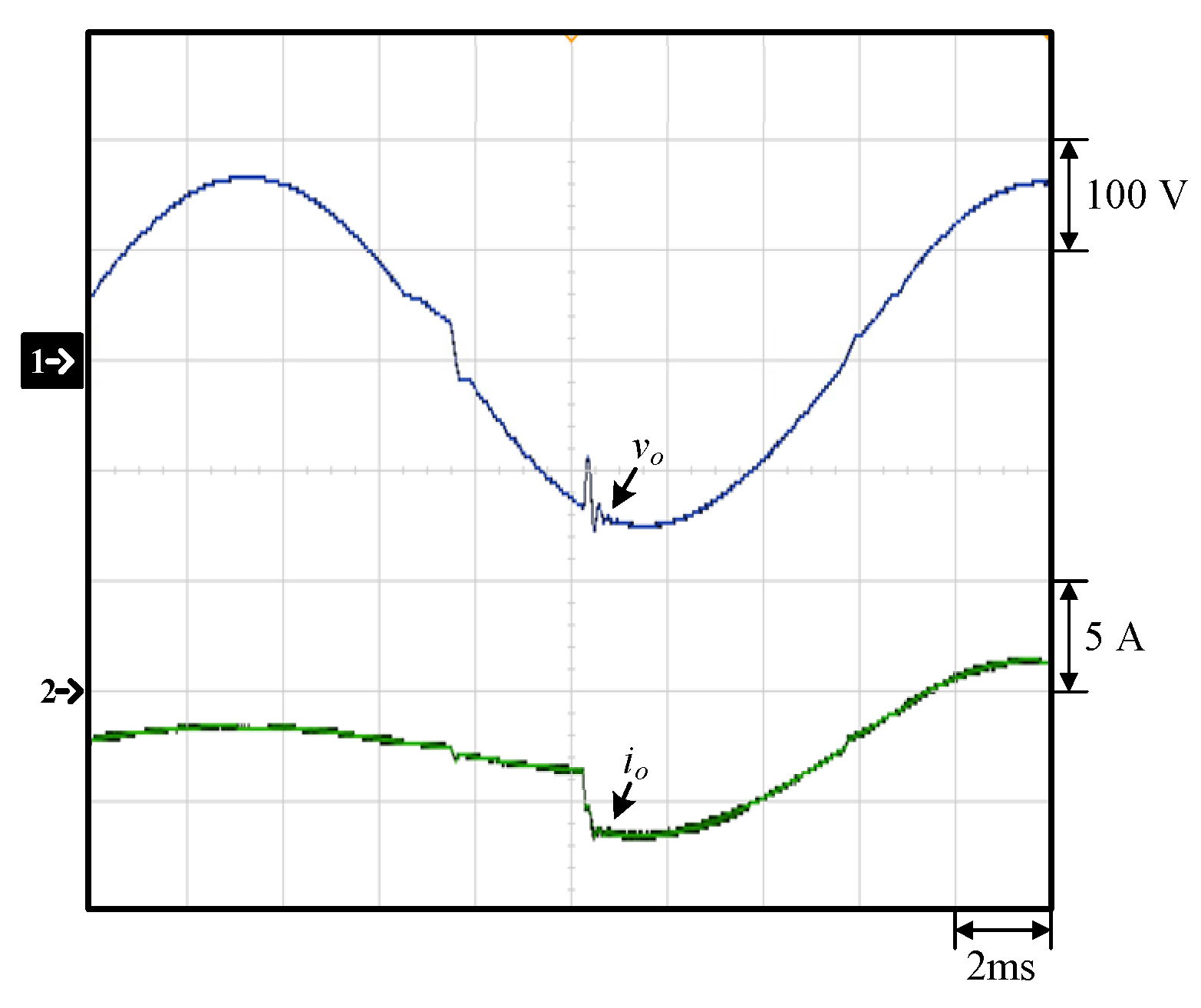
Figure 17 and Figure 18 show the distribution of voltage harmonics at rated and minimum load, respectively. The corresponding total harmonic distortion (THD) is 2.75% and 4.1% at rated and minimum load, respectively, as measured by a power meter. The proposed 7-level DC-AC converter can indeed comply with the specifications of IEEE 519-1992, which states that the corresponding THD is less than 5%. Figure 19 displays the load transient response due to step load current change from 25% to 100% load. From this figure, it can be seen that the overshoot voltage is about 50 V and the recovery time is about 0.6 ms.
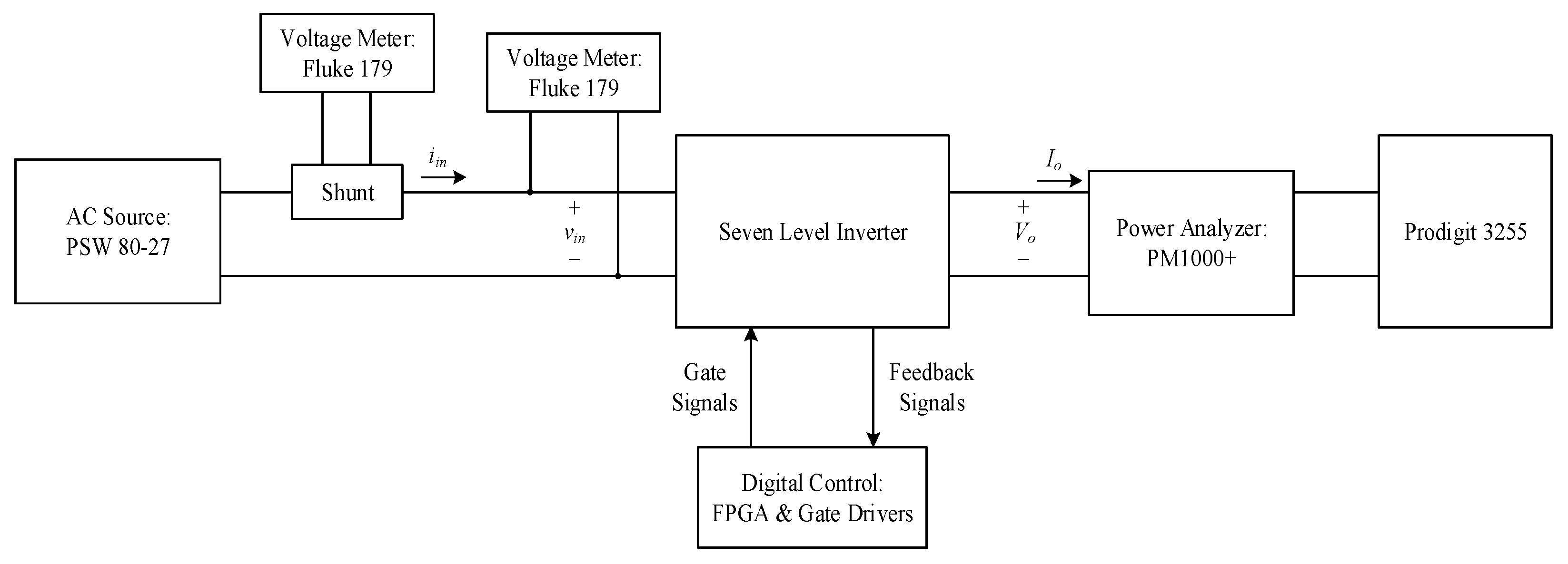
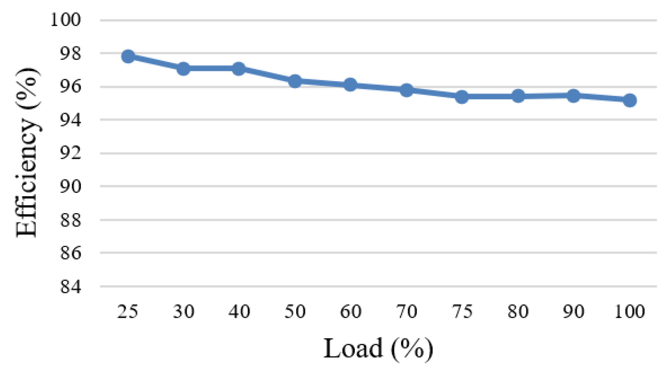
The efficiency of the proposed inverter under different loads is measured as shown in Figure 20. First, two digital meters, named Fluke 179, are used to measure the input voltage and the voltage across the current-detecting resistor, named shunt. Then, the output voltage, output current, total harmonic distortion, and harmonic voltage of each harmonic order are measured by using a power analyzer (PM1000+). Therefore, the input power and output power can be obtained. Moreover, the AC electronic load, named Prodigit 3255, is used at the load side. Finally, the obtained input power and output power are used to calculate the efficiency as shown in Figure 21. As can be seen in Figure 21, the proposed converter circuit belongs to a diode clamped circuit, causing the efficiency to be decreased when the load is higher.
6. Conclusions
This paper combines the Class-D amplifier and the conventional diode clamped DC-AC converter to create a single-voltage-source 3-voltage-gain 7-level DC-AC converter, where the DC link capacitors of the diode clamped DC-AC converter are used as energy-transferring capacitors to increase the output voltage and the number of levels. Due to the structure of this converter is symmetrical up and down, left and right, the interchangeability of mass production can be easily achieved. Furthermore, since only one switch operates at any time, not only the corresponding control is quite easy, but also any switch has very low switching voltage stress equal to the input voltage. Moreover, the proposed DC-AC converter has the highest conversion efficiency of 97.9% and the minimum THD of 2.75%, respectively.
Author Contributions
Conceptualization, J.-J.S., Y.-Y.L. and K.-I.H.; methodology, J.-J.S.; software, Y.-Y.L.; validation, Y.-Y.L., K.-I.H. and J.-J.S.; formal analysis, Y.-Y.L.; investigation, J.-J.S.; resources, Y.-Y.L.; data curation, J.-J.S.; writing—original draft preparation, K.-I.H.; writing—review and editing, K.-I.H.; visualization, J.-J.S.; supervision, K.-I.H.; project administration, K.-I.H.; funding acquisition, K.-I.H. and J.-J.S. All authors have read and agreed to the published version of the manuscript.
Funding
This research was funded by the Ministry of Science and Technology, Taiwan, under the Grant Number: MOST 110-2221-E-027-045-MY2.
Institutional Review Board Statement
No applicable.
Informed Consent Statement
No applicable.
Data Availability Statement
No new data were created or analyzed in this study. Data sharing is not applicable to this article.
Conflicts of Interest
The authors declare no conflict of interest.
References
- Erickson, R.W.; Maksimovic, D. Fundamental Power Electronics, 2nd ed.; Electronic Services; Springer: New York, NY, USA, 2001. [Google Scholar]
- IEC 61000-3-2; Electromagnetic Compatibility (EMC)-Part 3-2: Limits—Limits for Harmonic Current Emissions (Equipment Input Current ≤ 16 A per Phase). IEC: Geneva, Switzerland, 2005.
- JIS-C-61000-3-2; Electromagnetic Compatibility (EMC)-Part 3-2: Limits—Limits for Harmonic Current Emissions (Equipment Input Current ≤ 20 A per Phase). Japanese Standards Association: Tokyo, Japan, 2013.
- Nabae, A.; Takahashi, I.; Akagi, H. A new neutral-point-clamped PWM inverter. IEEE Trans. Ind. Appl. 1981, IA-17, 518–523. [Google Scholar] [CrossRef]
- Lai, J.-S.; Peng, F.Z. Multilevel converters-a new breed of power converters. IEEE Trans. Ind. Appl. 1996, 32, 509–517. [Google Scholar]
- Carrara, G.; Gardella, S.; Marchesoni, M.; Salutari, R.; Sciutto, G. A new multilevel PWM method: A theoretical analysis. IEEE Trans. Power Electron. 1992, 7, 497–505. [Google Scholar] [CrossRef]
- Siwakoti, Y.P. A new six-switch five-level boost-active neutral point clamped (5L-boost-ANPC) inverter. In Proceedings of the 2018 IEEE Applied Power Electronics Conference and Exposition (APEC), San Antonio, TX, USA, 4–8 March 2018; pp. 2424–2430. [Google Scholar]
- Lee, S.; Lim, C.S.; Lee, K.-B. Novel active-neutral-point-clamped inverters with improved voltage-boosting capability. IEEE Trans. Power Electron. 2019, 35, 5978–5986. [Google Scholar] [CrossRef]
- Wang, H.; Kou, L.; Liu, Y.-F.; Sen, P.C. A seven-switch five-level active-neutral-point-clamped converter and its optimal modulation strategy. IEEE Trans. Power Electron. 2017, 32, 5146–5161. [Google Scholar] [CrossRef]
- Dhanamjayulu, C.; Khasim, S.R.; Padmanaban, S.; Arunkumar, G.; Holm-Nielsen, J.B.; Blaabjerg, F. Design and implementation of multilevel inverters for fuel cell energy conversion system. IEEE Access 2020, 8, 183690–183707. [Google Scholar] [CrossRef]
- Liu, J.; Wu, J.; Zeng, J.; Guo, H. A novel nine-level inverter employing one voltage source and reduced components as high-frequency ac power source. IEEE Trans. Power Electron. 2016, 32, 2939–2947. [Google Scholar] [CrossRef]
- Liu, J.; Lin, W.; Wu, J.; Zeng, J. A novel nine-level quadruple boost inverter with inductive-load ability. IEEE Trans. Power Electron. 2019, 34, 4014–4018. [Google Scholar] [CrossRef]
- Zygmanowski, M.; Michalak, J.; Grzesik, B. DC-link voltage balancing method for a hybrid asymmetric multilevel converter. In Proceedings of the 2013 15th European Conference on Power Electronics and Applications (EPE), Lille, France, 2–6 September 2013; pp. 1–10. [Google Scholar]
- Hwu, K.I.; Yau, Y.T. Applying one-comparator counter-based PWM control strategy to DC-AC converter with voltage reference feedforward control considered. In Proceedings of the 2011 Twenty-Sixth Annual IEEE Applied Power Electronics Conference and Exposition (APEC), Fort Worth, TX, USA, 6–11 March 2011; pp. 1811–1815. [Google Scholar]
- IEEE Std 519-1992; IEEE Recommended Practices and Requirements for Harmonic Control in Electrical Power Systems. Intitute of Electronical and Electronics Engineers, Inc.: New York, NY, USA, 1993.
Figure 1.
DC-AC converter classification.

Figure 2.
Single-voltage-source Class-D 7-level DC-AC converter.

Figure 3.
Waveforms of the gate driving signals for switches.

Figure 4.
Gate driving signal for S1.

Figure 5.
Current flow direction of stage I when switch S1 is on.

Figure 6.
Current flow direction of stage I when switch S1 is off.

Figure 7.
Gate driving signal for S3.

Figure 8.
Current flow of stage II when switch S3 is on.

Figure 9.
Current flow direction of stage II when switch S3 is off.

Figure 10.
Gate driving signal for S10.

Figure 11.
Current flow direction of stage III when the switch S10 is on.

Figure 12.
Current flow direction of stage III when switch S10 is off.

Figure 13.
Charge of energy-transferring capacitors C1 and C4 during the discharge period.

Figure 14.
Filter circuit diagram for the output load.

Figure 15.
System block diagram of the proposed 7-level DC-AC converter.

Figure 16.
Simulated and experimental waveforms of the proposed DC-AC converter: (a) vo and io; (b) vo and vPWM; (c) VC1 and VC2; (d) VC3 and VC4.
Figure 16.
Simulated and experimental waveforms of the proposed DC-AC converter: (a) vo and io; (b) vo and vPWM; (c) VC1 and VC2; (d) VC3 and VC4.

Figure 17.
Distribution of harmonic voltages at rated load.

Figure 18.
Distribution of harmonic voltages at minimum load.

Figure 19.
Load transient response due to step load current change from 25% to 100% load: (1) vo; (2) io.
Figure 19.
Load transient response due to step load current change from 25% to 100% load: (1) vo; (2) io.

Figure 20.
Block diagram of efficiency measurement.

Figure 21.
Curve of efficiency versus load.


Table 1.
Switching behavior of the proposed 7-level DC-AC inverter.
| S1 | S3 | S4 | S9 | S10 | S12 | ||
|---|---|---|---|---|---|---|---|
| Switching Frequency | fpwm | fpwm | fline | fline | fpwm | fline | |
| Stage I | Switching type | 1, 0 | 0 | 1 | 1 | 0 | 1 |
| Maximum voltage stress | Vin | Vin | 0 | 0 | Vin | 0 | |
| Stage II | Switching type | 1 | 1, 0 | 1 | 1 | 0 | 1 |
| Maximum voltage stress | 0 | Vin | 0 | 0 | Vin | 0 | |
| Stage III | Switching type | 1 | 1 | 1 | 1 | 1, 0 | 1 |
| Maximum voltage stress | 0 | 0 | 0 | 0 | Vin | 0 | |
Table 2.
Specifications of the 7-level DC-AC converter.
| Input voltage (Vin) | 56 V |
| Output voltage (mains) frequency (fline) | 60 Hz |
| Output voltage (vo) | 110 Vrms |
| Rated output power (Po,rated)/Rated output current (Io,rated) | 300 W/2.72 Arms |
| Minimum output power (Po,min)/Minimum output current (Io,min) | 75 W/0.68 Arms |
| Switching frequency (fs) | 60 kHz |
Publisher’s Note: MDPI stays neutral with regard to jurisdictional claims in published maps and institutional affiliations. |
© 2022 by the authors. Licensee MDPI, Basel, Switzerland. This article is an open access article distributed under the terms and conditions of the Creative Commons Attribution (CC BY) license (https://creativecommons.org/licenses/by/4.0/).
Share and Cite
MDPI and ACS Style
Shieh, J.-J.; Hwu, K.-I.; Li, Y.-Y. A Single-Voltage-Source Class-D Boost Multi-Level Inverter with Self-Balanced Capacitors. Energies 2022, 15, 4082. https://0-doi-org.brum.beds.ac.uk/10.3390/en15114082
AMA Style
Shieh J-J, Hwu K-I, Li Y-Y. A Single-Voltage-Source Class-D Boost Multi-Level Inverter with Self-Balanced Capacitors. Energies. 2022; 15(11):4082. https://0-doi-org.brum.beds.ac.uk/10.3390/en15114082
Chicago/Turabian StyleShieh, Jenn-Jong, Kuo-Ing Hwu, and You-Yang Li. 2022. "A Single-Voltage-Source Class-D Boost Multi-Level Inverter with Self-Balanced Capacitors" Energies 15, no. 11: 4082. https://0-doi-org.brum.beds.ac.uk/10.3390/en15114082
Note that from the first issue of 2016, this journal uses article numbers instead of page numbers. See further details here.