
Current Source Converter as an Effective Interface to Interconnect Microgrid and Main Grid


1
College of Energy and Power Engineering, Inner Mongolia University of Technology, Hohhot 010051, China
2
School of Electrical and Information Engineering, Tianjin University, Tianjin 300072, China
*
Author to whom correspondence should be addressed.
Energies 2022, 15(17), 6447; https://0-doi-org.brum.beds.ac.uk/10.3390/en15176447
Submission received: 24 June 2022
/
Revised: 24 August 2022
/
Accepted: 25 August 2022
/
Published: 3 September 2022
(This article belongs to the Special Issue Advances in DC Technology for Modern Power Systems)
Abstract
:Back-to-back current source converters play an important role in high power applications. However, this back-to-back converter system uses a larger number of power switches, which is associated with more cost and the power density of the converter system can be affected. To address this issue, in this paper, a novel nine-switch back-to-back current source converter is proposed. To realize proper modulation of this nine-switch converter system, the concept of ampere balance is revisited at first. Then, its relationship with the traditional modulation scheme is revealed. Moreover, based on the ampere balance, the real-time dwell time calculation method is developed, where the tracking of rectifier current and inverter current is taken into consideration simultaneously. Finally, simulation results verify the effectiveness of the proposed modulation scheme.
1. Introduction
Current source converters have advantages such as motor-friendly waveforms, good short circuit protection ability, and low voltage change rate [1], it has been widely used in high power applications, such as the medium voltage drive systems and the high voltage dc transmission systems [2,3,4]. In recent years, using the current source converter as an effective interface between the main grid and microgrid has attracted much attention, as the current source converter can easily produce sinusoidal current without using any complex closed-loop current tracking [5,6]. In current source converters, symmetric gate-commutated thyristors or symmetric gate turn-off thyristors are popular choices. To construct a two-level back-to-back current source converter, 12 power switches are needed, which will result in a high cost and low power density. On the other hand, it has been reported that new topologies with only 9 switches have been applied to back-to-back voltage source converters [7,8,9]. Accordingly, it is necessary to study a similar nine-switch current source converter to replace the traditional back-to-back current source converter.
In the previous studies, different control and modulation schemes have been proposed for nine-switch voltage source converters [10,11,12]. In [10], the dual SPWM modulation was applied to control two output voltages with different frequencies and magnitude. In addition, in [10], the model predictive approach was proposed where the dwell time of each switch is directly calculated but the switching frequency is not fixed. For the traditional current source converter, the three-segment space vector modulation (SVM) is very popular due to its superior harmonic performance. In addition, some improved modulation methods such as natural sampling SVM [12,13] and multisampling SVM [14,15] have been also applied in the single converter or back-to-back current source converter for high power quality [11]. However, for the nine-switch current source converter, to the best of the authors’ knowledge, the corresponding SVM has not been reported so far. Because of the strong coupling between the rectifier side and inverter side, the traditional modulation SVM modulation approach cannot be directly used for nine-switch current source converters.
Motivated by the limitation of traditional SVM, a novel modulation strategy for a nine-switch current source converter is proposed in this paper. In this method, the calculation of dwell time is based on the ampere balance equation. Further, a cost function is designed to allocate dwell time among switches, which can minimize tracking errors. The rest of this paper is organized as follows. Section 2 explains the basic principle of ampere balance and reveals the relationship with SVM. In Section 3, the nine-switch current source converter is introduced, and the dwell time calculation method based on ampere balance is demonstrated. The modification to the dwell time is also given here. Then, in Section 4, simulation results are presented to verify the performance of the proposed modulation strategy. Finally, Section 5 concludes this paper.
2. Basic Principle of Ampere-Second Balance
The area equivalence method is widely used in the analysis of modulation for converters. With equal impulse and different shapes, the sinusoidal waveforms can be realized by using narrow pulses. In practical applications of voltage source converters, the three-phase sinusoidal modulation waveforms and carriers are used to generate gate signals, which can lead to an equivalent sinusoidal input voltage. Similarly, the sinusoidal current can also be guaranteed with the use of an LC filter in a current source converter. In this section, a direct PWM strategy is proposed based on the ampere-balance principle. The switching instants of each switch can be determined based on the conduction time.
Taking the current source rectifier as an example, the proposed ampere-balance modulation strategy is analyzed in detail. The basic topology of the current source rectifier is shown in Figure 1, where S1 to S6 represent six GCT switches. Idc represents the dc side current. In each phase, shunt capacitors with capacitance Cf are used to provide the commutation path and to filter out the switching ripple currents. The is the grid side choke inductance. The grid side current and converter side current of phase “a” are noted as isa and iwa, respectively. The current flow through switches S1 and S4 are represented with iw1 and iw4 respectively. Finally, for this type of system, a large dc choke with inductance Ldc is placed at the dc rail.
In the conventional modulation schemes for the current source converter, there is always a switch conducting for the whole switching cycle in each sector. In other words, the other two switches on the same side will be turned off, leading to a zero-conduction time. The sector number can be determined based on the angle of the reference current. The sector definition is given below.
where θ is the angle of the reference current in the α-β frame, and SN is the sector number, Tn is the conduction time of switch n in a switching cycle Ts.
Taking sector 1 as an example, the conduction time of S1 is Ts, and the conduction times of S2 and S3 are zeros. Hence, the initial values in this sector can be expressed as
Since the switching cycle Ts is short enough, the dc side current Idc can be regarded as a constant. The amplitude of iw1 and iw4 is Idc or zero, and the width of pulses is in a sinusoidal distribution, as shown in Figure 2. Since the LC filter is a second-order system, the harmonic components in the isa can be suppressed effectively, which can ensure the quality of grid side current. The amplitude of the grid side current is determined by the modulation index.
In a switching cycle, the relationship between the current flow through switches and the converter side current is expressed below.
where iwb and iwc are the converter side currents of phase “b” and phase “c”, respectively. In addition, the conduction time of each switch is defined as
The conduction time of S4, S2, and S6 can be obtained as
The dwell time of each switch in the other five sectors can be calculated similarly. To reveal the essential relationship between the ampere balance and SVPWM, the dwell time of the switch is analyzed in detail.
Assuming the current reference signals locate in sector 1, the three phase reference signals have the same amplitude with a 120° difference in phase angle. The expression of three phase current reference is given as
where Iwm is the peak value of the current reference, and ω is the angular frequency.
Then, the conduction time of S4, S6, and S2 in a switching cycle can be expressed as
In the standard SVPWM technique, the dwell time of current vectors are
where TSVM1, TSVM2, and TSVM0 are the dwell time of current vectors I1, I2, and I0, respectively. The modulation index m is defined as
Comparing (8) and (5), it can be concluded that
By comparing the results in ampere balance and standard SVPWM, the conclusion can be drawn as
- (1)
- The conduction time of S1 is Ts while the conduction time of S3 and S5 is zero, which is in accordance with that in the ampere balance method.
- (2)
- The dwell time of S4, S5, and S6 is consistent with the results in (5).
In conclusion, the conduction time calculation in the ampere balance method is equivalent to that in the SVPWM technique.
3. Nine-Switch Converter
The topology of the nine-switch current source converter is shown in Figure 3. This converter consists of nine switches, where S1 to S6 are responsible for the rectifier side and S4 to S9 are defined on the inverter side. More specially, S4 to S6 play a role in both the rectifier side and inverter side. Similarly, on the grid side, Cf1 and Ls are the CL filter per-phase shunt capacitance and series inductance, respectively. The grid side currents are represented with ia1, ib1, and ic1, while ia2, ib2, and ic2 denote the load currents on the inverter side. The reference direction of currents is demonstrated in Figure 3. Compared with traditional back-to-back current source converter, this nine-switch converter has the merits of small volume, simple structure, and increased power density.
As mentioned above, the modulation scheme is still a challenging task for this topology. For the widely used selective harmonic elimination (SHE) scheme in conventional current source converter, it is difficult to calculate the trigging angles of S4 to S6 due to the existing coupling between the rectifier side and inverter side. As for the traditional SVPWM technique, the conduction time of S4 to S6 cannot meet the requirements from the rectifier side and grid side if they are controlled independently. Thus, the performance of the rectifier side and inverter side must be taken into consideration simultaneously in the design of the modulation scheme.
3.1. Ampere Balance in Nine-Switch Converter
On the rectifier side, the current iwa1 is shaped by S1 and S4, iwb1 is shaped by S2 and S5, and iwc1 is shaped by S3 and S6. On the inverter side, S4 to S6 work with S7 to S9 to adjust the load side current. Applying the ampere balance equation to the nine-switch converter, the relationship between dwell time and reference signals can be expressed as
where T1 to T9 are the conduction time of S1 to S9, respectively, and Ts is the switching cycle.
When the current reference of the rectifier is located at sector 1, the initial values of T1 to T3 are
The conduction time of each switch must be non-negative, i.e.,
The conduction time of all switches can be obtained with a simple calculation, as shown in (15).
3.2. Conduction Time Modification
However, the results in (15) are the numerical solution, the limitation in (14) is not taken into consideration, which means T7 to T9 may be negative at some operating points. Under this case, the dwell time of each switching must be modified.
According to the number of negative dwell time, it can be divided into three cases, and the corresponding solution is discussed below.
Case one: All three switches have non-negative dwell time. At this time, the calculated dwell time can be implemented directly.
Case two: Only one switch has negative dwell time. Here the switch with negative dwell time is denoted as switch i, and the other two switches are denoted as switch j and switch k. First, the dwell time of switch i will be increased to zero. Since the summation of Ti, Tj, and Tk is Ts, the dwell time of switch j and switch k needs to be adjusted. To allocate the dwell time between switch j and switch k, an extra parameter Δ is introduced. The corresponding Ti, Tj, and Tk are expressed as
where Δ is in the range of 0 to 1 with a step of 0.1. On the other hand, the dwell time of S1 to S6 must be modified to minimize the tracking errors of converter currents. The modified dwell time is represented with T1m to T6m. Then, the limitation in (14) must be satisfied, and the summation dwell time of these three switches in the same row should be Ts.
The tracking error can be quantified with the error in conduction time. The error in each current is expressed as
A cost function can be defined to select the best Δ, as shown in (18).
This cost function can evaluate the tracking errors under each Δ. The Δ with minimal cost function value should be used.
Case three: There are two switches with negative dwell time. In this case, the dwell time of these two switches can be set to zero. For the other switch, its dwell time will be Ts, as shown below.
For case two and case three, the ampere-balance can only be satisfied to an extent, which will lead to tracking errors inevitably. However, the use of dwell modification and cost function can minimize the tracking errors.
3.3. Switching Sequence Design
For the nine-switch current source converter, it is necessary to design an optimal switching sequence for reducing harmonic and switching loss. For the simplicity of design, the switching sequences of S1 to S6 and S7 to S9 are designed separately.
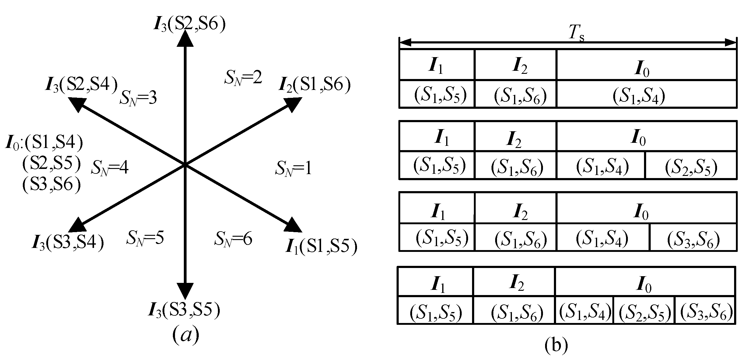
For the switching sequence of the rectifier side, the current vectors are used in a sequence of In-In+1-I0. The definition of current vectors is shown in Figure 4a. There are three zero current vectors in total, the selection of zero current vectors in each switching cycle is based on the minimal switching loss. Taking sector 1 as an example, the corresponding switching sequence is demonstrated in Figure 4b.
For the arrangement of S7 to S9, three sectors are divided based on the angle information, as shown in Figure 5. In sector I, the switching sequence is S7-S8-S9. In sector II and sector III, the orders are S8-S9-S7 and S9-S7-S8, respectively.
The overall diagram of the proposed modulation strategy for the nine-switch current source converter is given in Figure 6.
Step 1: Calculate the dwell time of each switch based on the current reference signals.
Step 2: Determine the number of negative dwell time. If no negative dwell exists, the dwell time can be used to generate gate signals directly (i.e., case one). If there is one switch with negative dwell time, extra parameter Δ and cost function will be used to modify the dwell time (i.e., case two). If there are two switches with negative dwell time, the dwell time must be rearranged in the way of (19).
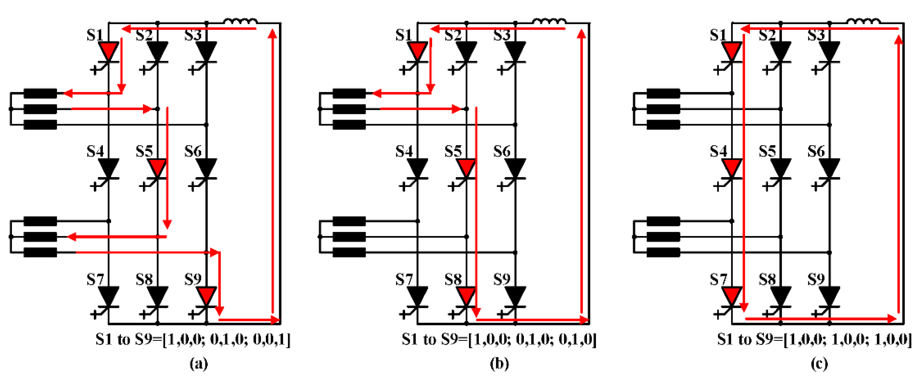
3.4. Current Path Analysis
To obtain a better understanding of the current path of the system. The performances of a few typical switching states are illustrated as shown below. First, when the state of S1 to S9 is [1, 0, 0; 0, 1, 0; 0, 0, 1], the current path is shown in Figure 7a. It can be seen that the dc rail current goes through S1 in the upper three switches, and the current flows to S5 in the middle switches via the upper ac circuit network. Then, the current goes to the lower circuit network and it goes back to the dc rail via S9. Similar current paths under different switching states can be analyzed similarly. Second, when the state of S1 to S9 is [1, 0, 0; 0, 1, 0; 0, 1, 0] as shown in Figure 7b, the dc rail current also goes through S1 and S5. However, it goes back to dc rail via S8, instead of S9. Last, when the state of S1–S9 is [1, 0, 0; 0, 1, 0; 1, 0, 0;], the dc rail current also flows through S1 in the upper switches but goes back to the dc rail through S4 and S7 in the middle and lower switches, respectively.
4. Simulation Verification
The proposed modulation strategy is verified in MATLAB/Simulink. The detailed parameters used in the simulation are listed in Table 1. On the rectifier side, the control loop is under the d-q frame. The dc side current is adjusted through a PI controller. In addition, to avoid the possible resonance of the CL filter, active damping based on capacitor voltage feedback is adopted.
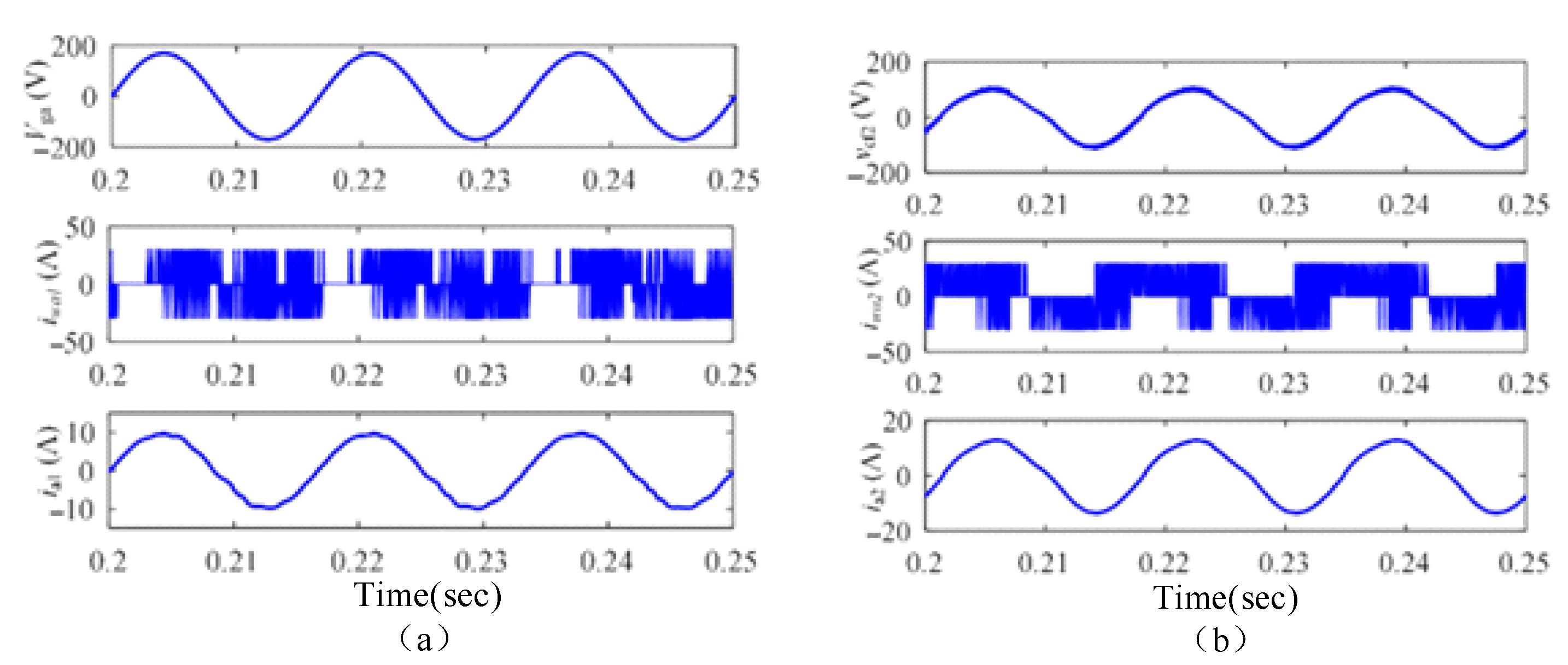
The steady performance under the same fundamental frequency is given in Figure 8. As shown, both the rectifier side and inverter side have a fundamental frequency of 60 Hz. In Figure 8a, from top to the bottom, the waveforms are grid voltage, converter current, and grid current, respectively. As expected, even when the output current of the rectifier has significant harmonic components, the grid current, in this case, is almost ripple-free, due to the adoption of the proposed SVM approach to reduce low order harmonics and the active damping approach for resonance mitigation. Accordingly, the THD of the grid current is only 3.75%, which can meet the grid code. The harmonic spectra of the rectifier side current are given in Figure 9.
On the inverter side, the performance of the load side converter is shown in Figure 10b. From top to the bottom, the waveforms are load side capacitor voltage, load side converter current, and load current, respectively. As the RL load is adopted in the simulation, the load current has good performance.
In Figure 10, the rectifier and the inverter are operated under different fundamental frequencies. The fundamental frequency of the rectifier side is 60 Hz, while the fundamental frequency of the inverter side is 30 Hz. In Figure 10a, from top to the bottom, the waveforms are grid voltage, converter current, and grid current, respectively. Figure 10b shows the results on the inverter side, where the waveforms are capacitor voltage, converter current, and load current, respectively. Some distortion can be found in the load current. As analyzed before, when the dc rail current is not high enough, the ampere balance will be broken at some points and it actually stands for the overmodulation operation of the system. Accordingly, it will inevitably cause distortion and ripple.
The dynamic performance is given in Figure 11, where the fundamental frequency of the inverter side changes from 60 Hz to 120 Hz at 0.2 s, while the fundamental frequency on the rectifier side is always 60 Hz. As it can be seen, the load currents can be stable within a very short time, while the rectifier side can maintain good performance at all times. With such good dynamic performance, the potential application of the nine-switch current source converter can be extended to a variable frequency motor drive.
5. Conclusions
Compared with the traditional back-to-back current source converter, the number of power semiconductor switches in the nine-switch current source is reduced. However, the traditional SVPWM modulation approach for back-to-back current source converters cannot be directly used by nine-switch current source converters. To address this issue, in this paper, a novel space vector modulation scheme is proposed and analyzed. First, the basic concept of ampere-balance is introduced, and then, the calculation and modification of the dwell time of each switch are realized based on the ampere-balance principle for both the rectifier side bridge and the inverter side bridge. Finally, the simulation results verified that the proposed modulation scheme has good harmonic performance and dynamic tracking ability.
Author Contributions
J.H., Y.X. and Y.R. jointly wrote the manuscript. H.W. and H.J. added some simulation verification results. All authors have read and agreed to the published version of the manuscript.
Funding
The National Natural Science Foundation of China, grant number 51967016 and 51567020.
Institutional Review Board Statement
Not applicable.
Informed Consent Statement
Not applicable.
Data Availability Statement
Not applicable.
Conflicts of Interest
The authors declare no conflict of interest.
References
- Li, Y.W. Control and Resonance Damping of Voltage-Source and Current-Source Converters with LC Filters. IEEE Trans. Ind. Electron. 2009, 56, 1511–1521. [Google Scholar]
- Perez, M.; Lizana, R.; Azocar, C.; Rodriguez, J.; Wu, B. Modular multilevel cascaded converter based on current source H-bridges cells. In Proceedings of the IECON 2012—38th Annual Conference on IEEE Industrial Electronics Society (IES), Montreal, QC, Canada, 25 October 2012. [Google Scholar]
- Liang, J.; Nami, A.; Dijkhuizen, F.; Tenca, P.; Sastry, J. Current source modular multilevel converter for HVDC and FACTS. In Proceedings of the 2013 15th European Conference on Power Electronics and Applications (EPE), Lille, France, 2 September 2013. [Google Scholar]
- Akhil, C.; Maiti, S. Power tapping from a current-source HVDC link using Modular Multilevel Converter. In Proceedings of the 2016 IEEE International Conference on Power Electronics, Drives and Energy Systems (PEDES), Trivandrum, India, 17 December 2016. [Google Scholar]
- Wei, Q.; Wu, B.; Xu, D.D.; Zargari, N.R. Optimal Space Vector Sequence Investigation Based on Natural Sampling SVM for Medium-Voltage Current-Source Converter. IEEE Trans. Power Electron. 2017, 32, 176–185. [Google Scholar] [CrossRef]
- Zhou, H.; Li, Y.W.; Zargari, N.R.; Cheng, Z.; Ni, R.; Zhang, Y. Selective Harmonic Compensation (SHC) PWM for Grid-Interfacing High-Power Converters. IEEE Trans. Power Electron. 2014, 29, 1118–1127. [Google Scholar] [CrossRef]
- Salem, A.; Narimani, M. Nine-Switch Current-Source Inverter-Fed Asymmetrical Six-Phase Machines Based on Vector Space Decomposition. In Proceedings of the 2020 IEEE Energy Conversion Congress and Exposition (ECCE), Detroit, MI, USA, 11 October 2020. [Google Scholar]
- Guedouani, R.; Fiala, B.; Boucherit, M.S. New PWM control strategy for multilevel three—Phase current source inverter. In Proceedings of the 4th International Conference on Power Engineering, Energy and Electrical Drives (POWERENG), Istanbul, Turkey, 13 May 2013. [Google Scholar]
- He, J.; Li, Q.; Wang, H.; Lyu, L.; Jia, H.; Wang, C. SVM Strategies for Simultaneous Common-Mode Voltage Reduction and DC Current Balancing in Parallel Current Source Converters. IEEE Trans. Power Electron. 2018, 33, 8859–8871. [Google Scholar] [CrossRef]
- Guazzelli, P.R.U.; de Castro, A.G.; dos Santos, S.T.C.A.; de Oliveira, C.M.R.; Pereira, W.C.A.; Monteiro, J.R.B.A.; de Aguiar, M.L. Dual Predictive Current Control of Grid Connected Nine-Switch Converter Applied to Induction Generator. In Proceedings of the 2018 13th IEEE International Conference on Industry Applications (INDUSCON), Sao Paulo, Brazil, 12 November 2018. [Google Scholar]
- Shang, J.; Li, Y.W. A Space-Vector Modulation Method for Common-Mode Voltage Reduction in Current-Source Converters. IEEE Trans. Power Electron. 2014, 29, 374–385. [Google Scholar] [CrossRef]
- Xu, D.; Wu, B. Multilevel Current Source Inverters with Phase Shifted Trapezoidal PWM. In Proceedings of the 2005 IEEE 36th Power Electronics Specialists Conference (PESC), Dresden, Germany, 16 June 2005. [Google Scholar]
- Wu, B.; Pontt, J.; Rodriguez, J.; Bernet, S.; Kouro, S. Current-Source Converter and Cycloconverter Topologies for Industrial Medium-Voltage Drives. IEEE Trans. Ind. Electron. 2008, 55, 2786–2797. [Google Scholar]
- Dai, J.; Lang, Y.; Wu, B.; Xu, D.; Zargari, N.R. A Multisampling SVM Scheme for Current Source Converters with Superior Harmonic Performance. IEEE Trans. Power Electron. 2009, 24, 2436–2445. [Google Scholar]
- Dai, J.; Xu, D.; Wu, B.; Zargari, N.R. Unified DC-Link Current Control for Low-Voltage Ride-Through in Current-Source-Converter-Based Wind Energy Conversion Systems. IEEE Trans. Power Electron. 2011, 26, 288–297. [Google Scholar]
Figure 1.
The topology of the current source rectifier.

Figure 2.
The output current waveform of the current source converter.

Figure 3.
Topology of the nine-switch current source converter.

Figure 4.
Switching sequence in the rectifier side for sector 1: (a) definition of current vectors; (b) switching sequence for sector 1.
Figure 4.
Switching sequence in the rectifier side for sector 1: (a) definition of current vectors; (b) switching sequence for sector 1.

Figure 5.
Switching sequence in the inverter side.

Figure 6.
An overall diagram of the proposed modulation strategy.

Figure 7.
Current path of the converter with different switching states: (a) S1 to S9 is [1, 0, 0; 0, 1, 0; 0, 0, 1]; (b) S1 to S9 is [1, 0, 0; 0, 1, 0; 0, 1, 0]; (c) S1 to S9 is [1, 0, 0; 0, 1, 0; 1, 0, 0].
Figure 7.
Current path of the converter with different switching states: (a) S1 to S9 is [1, 0, 0; 0, 1, 0; 0, 0, 1]; (b) S1 to S9 is [1, 0, 0; 0, 1, 0; 0, 1, 0]; (c) S1 to S9 is [1, 0, 0; 0, 1, 0; 1, 0, 0].

Figure 8.
Performance under the same fundamental frequency; (a) rectifier side, (b) inverter side.

Figure 9.
FFT results for rectifier side current.

Figure 10.
Performance under different fundamental frequency: (a) rectifier side (b) inverter side.

Figure 11.
Dynamic performance; (a) rectifier side, (b) inverter side.


Table 1.
Simulation parameters.
| Parameters | Values |
|---|---|
| Rated line voltage | 208 V |
| Inductors in the grid side | 3 mH |
| Filter capacitor | 150 μF |
| Dc side inductor | 30 mH |
| Inverter side RL load | 2 mH + 8 Ω |
| Sampling frequency | 5 kHz |
| Commutation time | 1 μs |
Publisher’s Note: MDPI stays neutral with regard to jurisdictional claims in published maps and institutional affiliations. |
© 2022 by the authors. Licensee MDPI, Basel, Switzerland. This article is an open access article distributed under the terms and conditions of the Creative Commons Attribution (CC BY) license (https://creativecommons.org/licenses/by/4.0/).
Share and Cite
MDPI and ACS Style
Xue, Y.; Ren, Y.; He, J.; Wang, H.; Jia, H. Current Source Converter as an Effective Interface to Interconnect Microgrid and Main Grid. Energies 2022, 15, 6447. https://0-doi-org.brum.beds.ac.uk/10.3390/en15176447
AMA Style
Xue Y, Ren Y, He J, Wang H, Jia H. Current Source Converter as an Effective Interface to Interconnect Microgrid and Main Grid. Energies. 2022; 15(17):6447. https://0-doi-org.brum.beds.ac.uk/10.3390/en15176447
Chicago/Turabian StyleXue, Yu, Yongfeng Ren, Jinwei He, Hao Wang, and Hongjie Jia. 2022. "Current Source Converter as an Effective Interface to Interconnect Microgrid and Main Grid" Energies 15, no. 17: 6447. https://0-doi-org.brum.beds.ac.uk/10.3390/en15176447
Note that from the first issue of 2016, this journal uses article numbers instead of page numbers. See further details here.