
Fabrication of Nanoscale Oxide Textured Surfaces on Polymers


1
Department of Chemical Engineering, Technion, Haifa 3200003, Israel
2
Shamir Optical Industry Ltd., Kibbutz Shamir, Upper Galilee 1213500, Israel
*
Author to whom correspondence should be addressed.
Polymers 2021, 13(13), 2209; https://0-doi-org.brum.beds.ac.uk/10.3390/polym13132209
Submission received: 15 June 2021
/
Revised: 30 June 2021
/
Accepted: 1 July 2021
/
Published: 3 July 2021
(This article belongs to the Section Polymer Processing and Engineering)
Abstract
:Nanoscale textured surfaces play an important role in creating antibacterial surfaces, broadband anti-reflective properties, and super-hydrophobicity in many technological systems. Creating nanoscale oxide textures on polymer substrates for applications such as ophthalmic lenses and flexible electronics imposes additional challenges over conventional nanofabrication processes since polymer substrates are typically temperature-sensitive and chemically reactive. In this study, we investigated and developed nanofabrication methodologies to create highly ordered oxide nanostructures on top of polymer substrates without any lithography process. We developed suitable block copolymer self-assembly, sequential infiltration synthesis (SIS), and reactive ion etching (RIE) for processes on polymer substrates. Importantly, to prevent damage to the temperature-sensitive polymer and polymer/oxide interface, we developed the process to be entirely performed at low temperatures, that is, below 80 °C, using a combination of UV crosslinking, solvent annealing, and modified SIS and RIE processes. In addition, we developed a substrate passivation process to overcome reactivity between the polymer substrate and the SIS precursors as well as a high precision RIE process to enable deep etching into the thermally insulated substrate. These methodologies widen the possibilities of nanofabrication on polymers.

1. Introduction
Oxide nanoscale structures play a central role in optical, electrical, and biomedical nanotechnological devices and sensors due to their tunable optoelectronic properties, high surface-to-volume ratio, and good stability [1,2]. In particular, surface texturing with high-aspect-ratio oxide nanostructures significantly enhances surface-based properties in sensors [3,4], antibacterial surfaces [5,6], hydrophobic surfaces [7], and optical lenses [8,9]. Oxide surface texturing has been demonstrated by several nanostructure formations and patterning techniques, including photolithography [10], nanoimprint lithography [11,12], colloid assembly [13,14], and mesoporous silica layers [15]. A high-aspect-ratio oxide nanostructure can enhance properties such as light transmission and surface hydrophobicity as well as act as an antireflective layer due to the low effective refractive index of the metal oxide/air sub-wavelength nanostructure [11]. If the nanostructure is designed to create an effective refractive index gradient, it can exhibit wide angular broadband anti-reflective behavior, such as moth eyes exhibit in nature and as has been mimicked by several man-made approaches [12,16,17,18,19,20,21,22,23].
Recent work has demonstrated oxide nanoscale structures on silicon substrates [23]. However, surface texturing of polymer substrates imposes new challenges compared to inorganic substrates due to additional constraints on the processing temperatures as well as polymer reactivity. With the growing demand for lightweight and cost-effective devices, there is a need for new nanofabrication processes for polymeric substrates [24].
In the past few decades, block copolymer (BCP) self-assembly has emerged as an excellent nanofabrication technique for simple and scalable nanoscale patterning [25,26,27,28,29]. BCP self-assembly yields highly ordered and uniform nanostructures with periodicity ranging between 10 and 100 nm [29]. BCP patterning is typically performed by casting a thin BCP layer on the substrate and annealing it to induce phase separation [28]. The BCP pattern can then be transferred to the underlying inorganic layer, resulting in a textured surface that can enhance hydrophobicity or anti-reflective properties [30,31]. However, pattern transfer of the BCP layer into high aspect ratio structures can impose a challenge due to the low etch contrast between typical BCP organic-organic domains.
Recently, sequential infiltration synthesis (SIS) has emerged as a novel technique for selectively growing metal oxides within the polar domain of block copolymers, enabling a high etch contrast between the blocks and efficient pattern transfer to form high-aspect-ratio structures [23,32,33,34,35,36]. SIS is based on atomic layer deposition (ALD) chemistry, where high precursor partial pressures and long exposure times result in precursors’ sorption and diffusion within the polymer [37]. The favorable interaction between the organometallic precursors and the polar domains of BCP can lead to the selective growth of metal oxides such as AlOx [35], ZnO [38], TiOx [39], and SnOx [40] in only one domain of the block copolymers [25,32,33,36]. Following the SIS process, the BCP film can be removed, resulting in a metal oxide nanostructure templated by the BCP morphology with high fidelity [25]. SIS has been successfully implemented into nanofabrication processes, such as semiconductor patterning [25,38], porous membrane fabrication [32,41,42], and anti-reflective layers [23,43].
Until now, SIS-based metal oxide nanostructures were fabricated onto silicon wafers or glass substrates, which are chemically inert and can withstand high-temperature processes. On the other hand, polymer substrates, such as diglycol, thiosulfonate, polycarbonate, and others, are not only sensitive to temperature but also can interact with the organometallic precursors used in the SIS process. Combining BCP self-assembly and SIS could offer a simple, scalable, and efficient way to fabricate high-aspect-ratio nanoscale oxide textures over a polymeric substrate.
In this study, we aim to expand SIS processes to polymer substrates and to enable nanoscale texturing of oxides onto polymers. Working with polymeric substrates poses a two-front challenge. First, there are competing temperature needs for optimal BCP assembly, SIS, and etching processing vs. the polymer substrate Tg and the polymer/oxide layer thermal expansion properties. Second, unlike silicon or glass inert substrates, polymers are potentially chemically reactive through outgassing or terminal edge moieties. The approach and methodologies developed in this work mitigate these challenges by using a combination of polymer substrate passivation processes to prevent undesired interactions between SIS precursors and the polymer substrates, room-temperature BCP assembly processes, and composite SIS patterning that overcomes pattern transfer challenges.
2. Experimental Details
2.1. Materials
BCP: polystyrene-block-poly(methyl methacrylate) (PS-b-PMMA) (Mn: 140k-b-65k, PDI = 1.16), (Mn:46.1k-b-21k, PDI = 1.09) (Mn: 68k-b-33.5k, PDI = 1.08), metalorganic precursors (trimethyl aluminum (TMA), diethyl zinc (DEZ)) and solvents (toluene, tetrahydrofuran, chloroform, etc.) were purchased from Polymer Source, STREM chemicals, and Fisher Scientific, respectively, and used as received.
2.2. Substrate Preparation
Discs of diglycol (MR-8TM), thiosulfonate (CR-39TM), and polycarbonate with a diameter and thickness of 20 mm and 2 mm, respectively, low resistivity (<0.005 Ω.cm) 4′′ Si (100) substrates, and glass slides were coated with 350 nm of SiO2 using chemical vapor deposition (MC380X box coater, Satisloh, Germantown, WI, USA) at Shamir Optics, Israel. SiO2/Si and SiO2/glass substrates were used as the reference standards. The surfaces of all the SiO2-coated substrates were cleaned in O2 plasma for 5 min prior to further processing.
2.3. BCP Templates
A thin layer of poly(styrene-r-methyl methacrylate-r-glycidyl methacrylate) (P(S-r-MMA-r-GMA)) containing ~4 mol% of glycidyl methacrylate with styrene mole fractions of 77% (PG-4 76%PS) was used for tuning the surface interactions of PS-b-PMMA with SiO2 substrate by spin-coating 0.3 wt. % of it in toluene. P(S-r-MMA-r-GMA) was synthesized by reversible addition fragmentation chain transfer polymerization with Azobisisobutyronitrile (AIBN), which is a thermal and photoinitiator. UV crosslinking was performed using Spectrolinker™ UV Crosslinkers (XL-1000 model) at a wavelength of 254 nm in N2 atmosphere. A layer of PMMA cylinder-forming PS-b-PMMA was fabricated by spin-coating 2 wt. % solution of PS-b-PMMA in toluene. The BCP layer was solvent vapor annealed (SVA) by exposing it to saturated vapors of tetrahydrofuran in a closed chamber containing ~100 mL of solvent at room temperature for durations ranging from 5 to 30 min. After exposure, the SVA was immediately quenched by taking it out of the annealing chamber, and the film was kept inside a fume hood for ~4 h to complete the evaporation of trapped THF vapors.
2.4. Sequential Infiltration Synthesis
AlOx and ZnO SIS were performed in a Savannah S100 ALD system (Veeco, New York, NY, USA). BCP films were loaded into the ALD reactor at 80 °C. To achieve thermal equilibrium and remove excess moisture, the samples were subjected to 20 sccm of N2 flow at 0.3 Torr for at least 30 min. The SIS process was carried out as follows: upon TMA pulse, the chamber was closed in a static mode for 300 s, enabling precursor diffusion into the polymer film (exposure). The exposure step was followed by an N2 purge step for 350 s to remove excess reactants. A similar exposure/purge process was used for water. The full AlOx SIS cycle, TMA/purge/H2O/purge = 300s/350s/300s/350s, was repeated several times. In a similar approach, AlOx/ZnO composite cylinders were fabricated by 2 cycles of AlOx SIS, followed by 6 cycles of ZnO SIS (DEZ/purge/H2O/purge) using the same sequence as AlOx SIS. After completion of the SIS process, the BCP template was removed by O2 plasma etching (50 W, 0.4 mbar for 10–20 min).
2.5. Passivation Process
The SiO2/polymer substrate was positioned over three adjacently placed Teflon discs to avoid the direct thermal contact of the polymer substrate with the ALD chamber. The passivation was performed by 100 cycles of Al2O3 ALD cycles using the following sequence: TMA exposure/purge/H2O exposure/purge for 10s /10s/10s/10s, respectively, at 80 °C.
2.6. Reactive Ion Etching
Vertically aligned SiO2 nanorods were fabricated by inductively coupled plasma-reactive ion etching using a Plasma-Therm (Oxford Instruments, Model: 790) with a CHF3 (5 sccm, 12 mTorr, 97 W rf power) and CF4 + O2 (36 sccm of CF4, 2 sccm of O2, 40 mTorr, 175 W rf power) mixture for different durations at room temperature.
2.7. Characterizations
The morphology of the sample was studied by a high-resolution scanning electron microscope (Ultra-Plus HRSEM, Zeiss, Oberkochen, Germany) at 1 kV. SEM cross-sectional samples on a SiO2/Si substrate were prepared by cleaving the substrate along a crystallographic direction. SiO2/polymer lenses were coated with 3 nm of Pt using BAF (Leica BAF 060) and cleaved after dipping them inside liquid nitrogen. Cross-section images were recorded by tilting the sample by 70°.
3. Results and Discussion
3.1. Process Overview
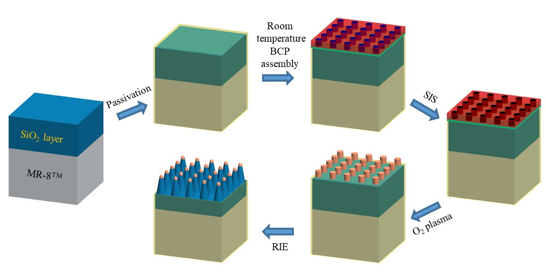
The fabrication methodology and processes for the nanoscale texturing of oxide layers on polymer substrates are schematically illustrated in Figure 1. The process was designed to enable the desired interaction between the BCP layer and SIS precursors while hindering interactions between these precursors and the polymer substrate. MR-8TM was chosen as the polymer substrate model system due to its wide use in ophthalmic lenses. Other polymer substrates that were examined, CR-39TM and polycarbonate, gave similar results, but for simplicity, we used MR-8TM as a model system. (1) First, we performed an ALD passivation process on the SiO2/MR-8TM polymer substrate to passivate the polymer substrate and prevent undesired interactions in the SIS stage. (2) We self-assembled polystyrene-block-poly(methyl methacrylate) (PS-b-PMMA) thin films on the passivated SiO2/MR-8TM polymer substrates using a room-temperature process, which includes random copolymer mat UV crosslinking to neutralize the interaction between the SiO2 surface and the BCP layer [44], followed by BCP solvent vapor annealing (SVA) to promote BCP self-assembly. (3) We selectively grew AlOx and ZnO in the cylindrical PMMA domains with the AlOx/ZnO SIS process. Following SIS, we removed the polymer template with oxygen plasma to obtain AlOx/ZnO composite nanorods that can be used as a hard mask for deep reactive ion etching (RIE). (4) We performed an RIE process to break through the Al2O3 passivation layer and transfer the AlOx/ZnO nanorod hard masks into the underlying SiO2 layer. The main steps of this process on non-sensitive substrates, SiO2/Si and SiO2/glass, are presented in Figures S1 and S2.
3.2. Room-Temperature BCP Assembly
3.2.1. Random Copolymer Mat Crosslinking Using UV Treatment
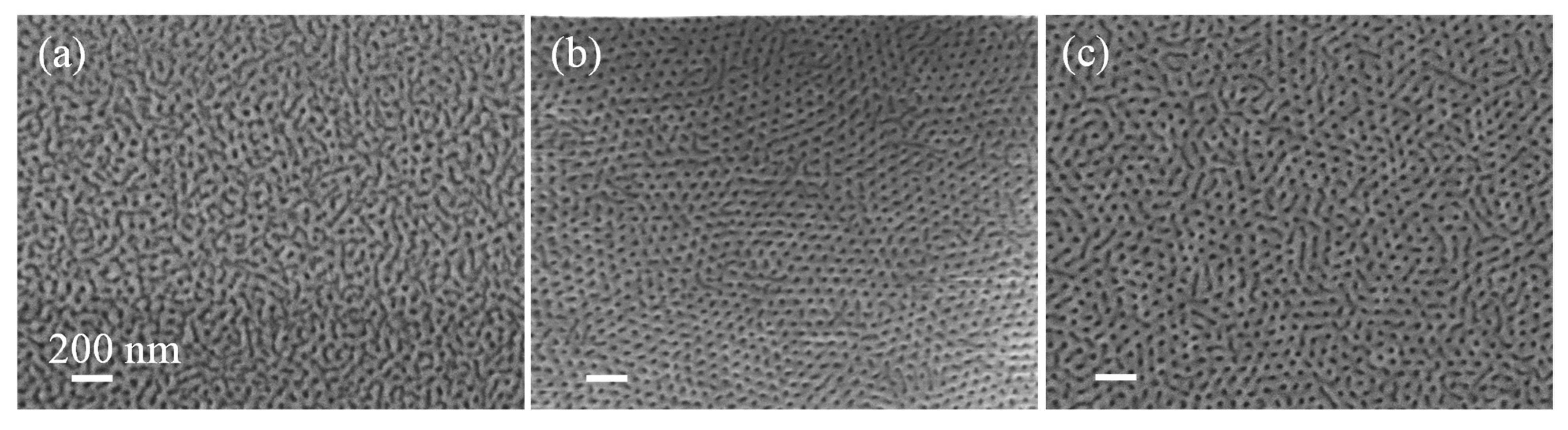
Oxide surfaces, such as SiO2 and Al2O3, are favorably wetted by the polar domains of BCP [45]. To induce vertical-oriented assembly, random copolymer mats are commonly used to create a surface that is wetted by both blocks [46]. The required polymer mat layer crosslinking is typically performed with thermal annealing at elevated temperatures (190 °C–250 °C). For example, Figure S3 shows the highly ordered perpendicular orientated self-assembly of PS-b-PMMA 46.1k-b-21k on a thermally (230 °C) crosslinked PG-4 76% mat. To create a room-temperature BCP assembly process, we first probed room-temperature polymer mat crosslinking using UV exposure (λ = 254 nm) in an inert environment. PG-4 mats are known to be UV crosslinkable due to the presence of epoxy side groups [47].
The mat layer quality of SiO2/Si using the self-assembly of an ~80 nm thick PS-b-PMMA 140k-b-65k film treated with 15 min of tetrahydrofuran (THF) SVA was examined. Figure 2 presents the resulting PS-b-PMMA morphology as a function of UV treatment. The dark domains correspond to PMMA, while the bright domains correspond to PS. When the random copolymer mat, PG-4 76%, was not treated with UV, the resulting PS-b-PMMA assembly lacked long-range order (Figure 2a). Applying a short, 20 sec UV treatment of a 120 mJ/cm2 dose led to the BCP self-assembly of perpendicular-orientated PMMA cylinders with 42 ± 4 nm diameters and an average grain size of 202 ± 6 nm (Figure 2b). Extensive UV treatment (1 h of exposure with a dose of 27,100 mJ/cm2; Figure 2c), resulted in perpendicular assembly but with a lower degree of long-range order.
3.2.2. BCP Solvent Annealing
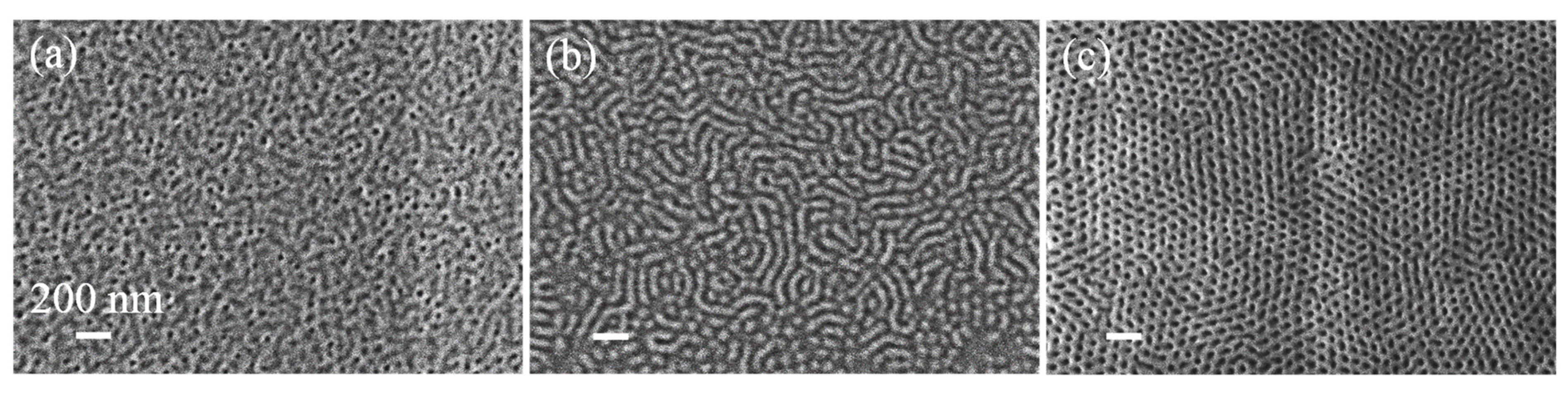
In order to establish a room-temperature BCP assembly process, we optimized the SVA process for PS-b-PMMA 140k-b-65k. Vapor infiltration into the polymer film leads to higher chain mobility due to polymer plasticization. It lowers the glass transition temperatures (Tg) and the effective Flory–Huggins parameter of the blocks (χeff < χ), as well as creating interface interaction screening, resulting in room-temperature BCP assembly [46,48,49,50,51]. Figure 3 shows the surface morphology of ~80 nm thick PS-b-PMMA 140k-b-65k after 15 min of SVA using chloroform, acetone, and THF. While chloroform and acetone SVA resulted in disordered assembly and parallel cylinder assembly, respectively (Figure 3a,b), THF SVA resulted in perpendicular PMMA cylinder assembly with 71 ± 2 nm periodicity and a high degree of order. THF is considered a good solvent for both blocks [49,52], swelling both blocks and creating similar effective interfacial energies that lead to perpendicular assembly. Interestingly, when the THF SVA is performed for longer or shorter times than 15 min, the assembly becomes disordered (Figure S4). This “sweet spot” time interval indicates that short SVA might be insufficient to swell both blocks, while long SVA could lead to non-uniform surface interactions due to the differences in polymer block/solvent interactions (χPS-THF = 0.32 and χPMMA-THF = 0.8) [53].
3.2.3. SIS on BCP/SiO2/MR-8 Polymer
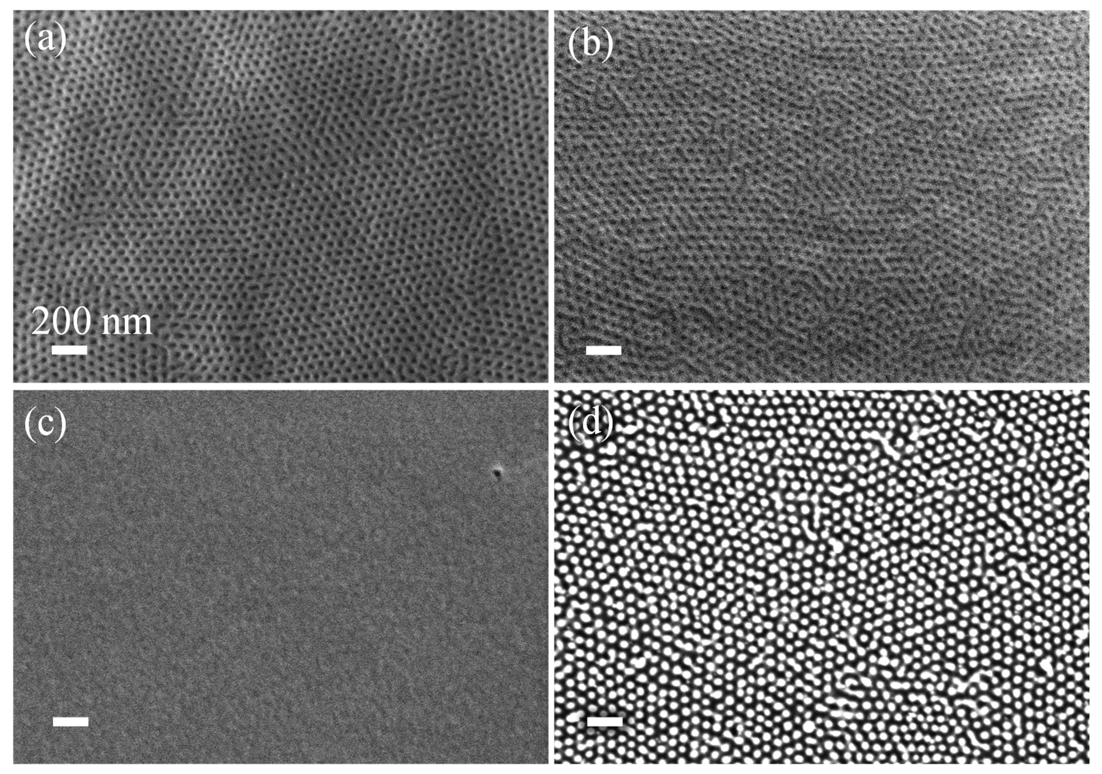
In order to develop oxide nano-textured surfaces on polymeric substrates, we examined the SIS process on BCP/SiO2/MR-8TM polymer stacks. A 500 nm SiO2 layer was deposited on an MR-8TM substrate with physical vapor deposition. The prepared substrates (SiO2/MR-8TM) were then coated with PG4 76% mat and PS-b-PMMA 140k-b-65k layers, as described in Section 2. BCP assembly on the top of SiO2/MR-8TM substrates displayed hexagonally ordered perpendicular PMMA cylinders in a PS matrix (Figure 4a). The thermal stability of the BCP layer was confirmed by placing BCP/SiO2/MR-8 samples at 80 °C for 3 h in the ALD chamber without any reaction (Figure 4b). The retention of the BCP self-assembled structure and the absence of SiO2/MR-8 polymer degradation during thermal treatment make the PS-b-PMMA/SiO2/MR-8 stack compatible for the SIS process. However, when we performed between one and eight cycles of AlOx SIS on the PS-b-PMMA/SiO2/MR-8TM stack, no traces of the self-assembled BCP layer nor a hybrid AlOx-BCP layer (Figure 4c) could be identified on the surface.
In comparison, when the same SIS process on PS-b-PMMA/SiO2/Si and PS-b-PMMA/SiO2/glass stacks was performed without the presence of the MR-8TM polymer substrate, selective growth of AlOx within the PMMA cylinders could easily be observed. Subsequent etching of the BCP film on SiO2/Si substrate with O2 plasma resulted in an ordered AlOx nanocylinders array, templated by the PMMA domains, with 42 ± 4 nm diameter AlOx cylinders (Figure 4d and Figure S1). Moreover, when these nanocylinder arrays were used as hard masks for RIE of the underlying SiO2 layer on Si or glass substrates, textured SiO2 surfaces with tunable-aspect-ratio SiO2 nanorods were obtained (Figures S2 and S5). The vertical AlOx nanocylinders and the resulting SiO2 nanorods indicate that the PMMA is vertically assembled in the BCP layer and that the SIS process efficiently grew AlOx in the PMMA domains.
While SIS on BCP/SiO2/Si and on BCP/SiO2/glass substrates resulted in selective growth of AlOx within the PMMA domains, SIS processes on the BCP/SiO2/MR-8 polymer substrate did not yield any ordered structure on the top surface. Other polymer substrates that were examined, CR-39TM, and polycarbonate, also exhibited the same behavior. We attribute this phenomenon to interactions of the organometallic precursor, TMA, with reactive moieties in the polymer substrate. For example, MR-8TM polymer has an abundance of reactive groups, such as hydroxyl and cyano groups, which can react with TMA and release byproduct molecules. These molecules can partly be deposited on the top BCP layer, obscuring the self-assembled layer and hindering SIS growth within the PMMA domains. SEM characterization of the post-SIS surface and scratching tests (data not shown) indicated the presence of additional organic materials at the top surface.
To overcome this limitation and enable SIS-based patterning on polymer substrates, we performed a surface passivation process. The SiO2/MR-8TM substrate, prior to random copolymer mat and BCP deposition, was exposed to 100 cycles of Al2O3 ALD (80 °C, TMA/purge/H2O/purge = 10s/10s/10s/10s), resulting in Al2O3 deposition on the SiO2/MR-8TM surface (see illustration in Figure 1). Figure 5 displays SEM imaging of PS-b-PMMA 140k-b-65k self-assembly and SIS processes on passivated SiO2/MR-8TM substrates. Following passivation, we self-assembled PS-b-PMMA 140k-b-65k on the crosslinked random copolymer mat, as described in Section 2, resulting in highly ordered perpendicular cylinder morphology (Figure 5a). Eight cycles of AlOx SIS on the self-assembled layer resulted in selective growth of AlOx in the PMMA domains, as can be seen from the reverse in contrast to the BCP domains (Figure 5b). We also examined the AlOx/ZnO SIS process, where two cycles of AlOx SIS were performed to promote ZnO growth in the PMMA domains using six cycles of ZnO SIS. When we removed the BCP layer using oxygen plasma, we obtained highly ordered AlOx and AlOx/ZnO nanorod arrays on the passivated SiO2/MR-8TM substrates (Figure 5c and Figure 5d, respectively). A cross-sectional SEM image of AlOx/ZnO nanorod arrays is presented as an inset of Figure 5d. The nanorods are estimated to be 25–35 nm in height and 35–40 nm in width. These BCP-templated metal oxide nanorods can now be used as a hard mask for pattern transfer to the underlying SiO2 layer.
3.2.4. Pattern Transfer into SiO2 Underlying Layer
In order to transfer the BCP-templated metal oxide structure into the SiO2 layer, we performed CHF3 RIE, which is known for its anisotropic etch of SiO2 and good Al2O3/SiO2 selectivity [54,55]. However, due to the SiO2/MR-8TM passivation, there was a nanometric Al2O3 layer between the metal oxide nanorods that needed to be etched to reach the SiO2 layer. When we performed CHF3 RIE on AlOx nanorods/Al2O3/SiO2/MR-8TM, the etch budget in the AlOx nanorods was insufficient to enable Al2O3 passivation breakthrough and maintain an efficient hard mask for SiO2 etching. On the other hand, when we performed CHF3 RIE on AlOx/ZnO composite nanorods/Al2O3/SiO2/MR-8TM, the higher etch resistance of the AlOx/ZnO composite nanorods enabled the nanorod to maintain its structure through the Al2O3 passivation breakthrough etch, leading to efficient pattern transfer.
We further developed the RIE process to account for the low thermal conductivity of the polymer substrate. Figure 6a,b present SEM images of the SiO2 surface formed after exposing the BCP-templated AlOx/ZnO nanorods to two modes of CHF3 RIE: continuous RIE for 3 min (Figure 6a), and loop RIE for 14 min, which is built from loops of 30 s of RIE and a 1 min purge (Figure 6b). The continuous 3 min etching resulted in shallow SiO2 texturing, as implied by the low contrast of the structure. The low thermal conductivity of the polymer substrate surface leads to substrate heating, enhancing isotropic etching, which results in nanocylinder mask etching. The loop RIE process, on the other hand, provides sufficient time between the plasma periods to dissipate the heat generated on the surface. Figure 6b clearly shows the intactness of the hexagonally ordered cylindrical array formed after the loop RIE. The corresponding cross-sectional image (Figure 6c) shows ~80 nm high and ~40 nm wide (~2:1 aspect ratio) oval-shaped nanorods, fabricated in the SiO2 layer by room-temperature BCP self-assembly, AlOx/ZnO SIS, and loop RIE. Further optimization of RIE chemistry for deep and/or conical-shaped high-aspect-ratio nanostructures is viable using the methodology presented in Figure S5.
4. Conclusions
In this research, a new methodology for creating highly ordered and periodic, nanoscale oxide texture on top of polymeric substrates was developed. These nanoscale textures can be used to enhance various properties, such as anti-reflectiveness and superhydrophobicity. The texturing is based on transferring the pattern of BCP onto metal oxide nanorods via SIS and onto the oxide layer via RIE. Our approach provided solutions to the challenges that nanoscale oxide texturing of polymer substrates poses. We have developed a series of suitable low-temperature (<80 °C) processes geared towards temperature-sensitive substrates. The polymer substrates were 3D-passivated with an ALD-processed Al2O3 barrier layer. On top of preventing undesired interactions between the SIS organometallic precursors and the polymer substrates, the passivation layer can be used as a general basis layer, reducing the need to tune the process for each polymer substrate chemistry. In addition, in order to enable a differential etch rate in the RIE step, an AlOx/ZnO composite was generated in the PMMA cylinder phase. This combined barrier-differential etch approach expands the standard SIS toolbox to enable new pathways for nanofabrication on a wide array of lighter-weight polymers over traditional SIS-processed glass and silicon substrates.
Supplementary Materials
The following are available online at https://0-www-mdpi-com.brum.beds.ac.uk/article/10.3390/polym13132209/s1. Figure S1: SEM images of AlOx cylinders pattern formed on (a) SiO2/Si substrate and (b) SiO2/glass substrate; Figure S2: Top (a,c) and cross-sectional (b,d) SEM images of SiO2 nanostructures formed by etching the AlOx nanocylinder pattern on SiO2/Si substrate (a,b) and SiO2/glass substrate (c,d) using 10 min CHF3 RIE; Figure S3: Top view SEM image of (a) PS-b-PMMA (46.1k-b-21k) block/copolymer after thermal annealing at 230 °C; Figure S4: SEM image of PS-b-PMMA (140k-b-65k) over SiO2/Si substrate vapor annealed for 10 and 20 min in tetrahydrofuran; Figure S5: SEM image of SiO2 nanorods array fabricated by different RIE chemistry: anisotropic etching of SiO2 by CHF3 (a) 5 min, (b) 10 min; isotropic etching of SiO2 by CF4 + O2 (c) 3 min, (d) 4 min, and combination of CHF3 and CF4 +O2 (e) 5 min and 1 min, (d) 10 min and 0.5 min, respectively.
Author Contributions
Conceptualization, T.S.-P. and U.G.; methodology, B.K.B. and N.S.; software, B.K.B.; validation, T.S.-P., U.G. and Z.K.; formal analysis, B.K.B.; investigation, B.K.B. and N.S.; resources, T.S.-P. and Z.K.; data curation, B.K.B.; writing—original draft preparation, B.K.B.; writing—review and editing, T.S.-P.; visualization, B.K.B.; supervision, T.S.-P.; project administration, T.S.-P. and U.G.; funding acquisition, T.S.-P., Z.K. and U.G. All authors have read and agreed to the published version of the manuscript.
Funding
This research was funded by the Israel Innovation Authority, NOFAR Program, Israel, grant number 65806 and by Shamir Opitcal Industry Ltd.
Institutional Review Board Statement
Not applicable.
Informed Consent Statement
Not applicable.
Data Availability Statement
Data available in a publicly accessible repository.
Acknowledgments
We acknowledge the Technion Center for Electron Microscopy of Soft Matter, Faculty of Chemical Engineering, and Nanoelectronics Research Center, Technion, for providing electron microscopy and nanofabrication facilities, respectively. B.K.B. gratefully acknowledges the Lady Davis Foundation for Lady Davis post-doctoral Fellowship.
Conflicts of Interest
The authors declare no conflict of interest.
References
- Ghenadii, K.; Daniela, N.; Ana, P.; Lidia, S.; Pedro, B.; Luis, P.; Elvira, F.; Rodrigo, M. Metal Oxide Nanostructures Synthesis; Properties and Applications Available online; Elsevier: Amsterdam, The Netherlands, 2018. [Google Scholar]
- Djurišić, A.B.; Chen, X.; Leung, Y.H.; Man Ching Ng, A. ZnO Nanostructures: Growth, Properties and Applications. J. Mater. Chem. 2012, 22, 6526. [Google Scholar] [CrossRef]
- Clavijo, W.P.; Atkinson, G.M.; Castano, C.E.; Pestov, D. Novel Low-Temperature Fabrication Process for Integrated High-Aspect Ratio Zinc Oxide Nanowire Sensors. J. Vac. Sci. Technol. B 2016, 34, 022203. [Google Scholar] [CrossRef]
- Ahmad, R.; Tripathy, N.; Ahn, M.-S.; Hahn, Y.-B. Solution Process Synthesis of High Aspect Ratio ZnO Nanorods on Electrode Surface for Sensitive Electrochemical Detection of Uric Acid. Sci. Rep. 2017, 7, 46475. [Google Scholar] [CrossRef] [PubMed]
- Bauer, L.A.; Birenbaum, N.S.; Meyer, G.J. Biological Applications of High Aspect Ratio Nanoparticles. J. Mater. Chem. 2004, 14, 517–526. [Google Scholar] [CrossRef]
- Tripathy, A.; Sen, P.; Su, B.; Briscoe, W.H. Natural and Bioinspired Nanostructured Bactericidal Surfaces. Adv. Colloid Interface Sci. 2017, 248, 85–104. [Google Scholar] [CrossRef] [PubMed]
- Ghanashyam Krishna, M.; Vinjanampati, M.; Dhar Purkayastha, D. Metal Oxide Thin Films and Nanostructures for Self-Cleaning Applications: Current Status and Future Prospects. Eur. Phys. J. Appl. Phys. 2013, 62, 30001. [Google Scholar] [CrossRef] [Green Version]
- Cai, J.; Qi, L. Recent Advances in Anti-reflective Surfaces Based on Nanostructure Arrays. Mater. Horiz. 2014, 2, 37–53. [Google Scholar] [CrossRef]
- Ye, X.; Jiang, X.-D.; Huang, J.; Sun, L.-X.; Geng, F.; Yi, Z.; Zu, X.-T.; Wu, W.-D.; Zheng, W. Subwavelength Structures for High Power Laser Antireflection Application on Fused Silica by One-Step Reactive Ion Etching. Opt. Lasers Eng. 2016, 78, 48–54. [Google Scholar] [CrossRef]
- Bacon-Brown, D.A.; Braun, P.V. Tunable Antireflection Coating to Remove Index-Matching Requirement for Interference Lithography. Adv. Opt. Mater. 2018, 6, 1701049. [Google Scholar] [CrossRef]
- Kumar Raut, H.; Anand Ganesh, V.; Sreekumaran Nair, A.; Ramakrishna, S. Anti-Reflective Coatings: A Critical, in-Depth Review. Energy Environ. Sci. 2011, 4, 3779–3804. [Google Scholar] [CrossRef]
- Kuo, W.-K.; Hsu, J.-J.; Nien, C.-K.; Yu, H.H. Moth-Eye-Inspired Biophotonic Surfaces with Anti-reflective and Hydrophobic Characteristics. ACS Appl. Mater. Interfaces 2016, 8, 32021–32030. [Google Scholar] [CrossRef]
- Lee, K.; Kreider, M.; Bai, W.; Cheng, L.-C.; Dinachali, S.S.; Tu, K.-H.; Huang, T.; Ntetsikas, K.; Liontos, G.; Avgeropoulos, A.; et al. UV-Solvent Annealing of PDMS-Majority and PS-Majority PS-b-PDMS Block Copolymer Films. Nanotechnology 2016, 27, 465301. [Google Scholar] [CrossRef]
- Wang, L.; Fu, Y.; Wang, Z.; Fan, Y.; Zhang, X. Investigation into an Alternating Multilayer Film of Poly(4-Vinylpyridine) and Poly(Acrylic Acid) Based on Hydrogen Bonding. Langmuir 1999, 15, 1360–1363. [Google Scholar] [CrossRef]
- Jin, B.; He, J.; Yao, L.; Zhang, Y.; Li, J. Rational Design and Construction of Well-Organized Macro-Mesoporous SiO2/TiO2 Nanostructure toward Robust High-Performance Self-Cleaning Antireflective Thin Films. ACS Appl. Mater. Interfaces 2017, 9, 17466–17475. [Google Scholar] [CrossRef] [PubMed]
- Ji, S.; Park, J.; Lim, H. Improved Antireflection Properties of Moth Eye Mimicking Nanopillars on Transparent Glass: Flat Antireflection and Color Tuning. Nanoscale 2012, 4, 4603–4610. [Google Scholar] [CrossRef]
- Phillips, B.M.; Jiang, P. Chapter 12—Biomimetic Antireflection Surfaces. In Engineered Biomimicry; Lakhtakia, A., Martín-Palma, R.J., Eds.; Elsevier: Boston, MA, USA, 2013; pp. 305–331. [Google Scholar]
- Li, J.; Zhu, J.; Gao, X. Bio-Inspired High-Performance Antireflection and Antifogging Polymer Films. Small 2014, 10, 2578–2582. [Google Scholar] [CrossRef] [PubMed]
- Han, S.-Y.; Paul, B.K.; Chang, C. Nanostructured ZnO as Biomimetic Anti-Reflective Coatings on Textured Silicon Using a Continuous Solution Process. J. Mater. Chem. 2012, 22, 22906–22912. [Google Scholar] [CrossRef]
- Raut, H.K.; Dinachali, S.S.; He, A.Y.; Ganesh, V.A.; Saifullah, M.S.M.; Law, J.; Ramakrishna, S. Robust and Durable Polyhedral Oligomeric Silsesquioxane-Based Antireflective Nanostructures with Broadband Quasi-Omnidirectional Properties. Energy Environ. Sci. 2013, 6, 1929–1937. [Google Scholar] [CrossRef]
- Baquedano, E.; Torné, L.; Caño, P.; Postigo, P.A. Increased Efficiency of Solar Cells Protected by Hydrophobic and Hydrophilic Anti-Reflecting Nanostructured Glasses. Nanomaterials 2017, 7, 437. [Google Scholar] [CrossRef] [Green Version]
- Xie, G.; Zhang, G.; Lin, F.; Zhang, J.; Liu, Z.; Mu, S. The Fabrication of Subwavelength Anti-Reflective Nanostructures Using a Bio-Template. Nanotechnology 2008, 19, 095605. [Google Scholar] [CrossRef]
- Rahman, A.; Ashraf, A.; Xin, H.; Tong, X.; Sutter, P.; Eisaman, M.D.; Black, C.T. Sub-50-Nm Self-Assembled Nanotextures for Enhanced Broadband Antireflection in Silicon Solar Cells. Nat. Commun. 2015, 6, 5963. [Google Scholar] [CrossRef] [PubMed] [Green Version]
- Kingslake, R.; Barry Johnson, R. Chapter 1—The Work of the Lens Designer. In Lens Design Fundamentals (Second Edition); Kingslake, R., Barry Johnson, R., Eds.; Academic Press: Boston, MA, USA, 2010; pp. 1–23. [Google Scholar]
- Peng, Q.; Tseng, Y.-C.; Darling, S.B.; Elam, J.W. A Route to Nanoscopic Materials via Sequential Infiltration Synthesis on Block Copolymer Templates. ACS Nano 2011, 5, 4600–4606. [Google Scholar] [CrossRef] [PubMed]
- Leng, C.Z.; Losego, M.D. Vapor Phase Infiltration (VPI) for Transforming Polymers into Organic–Inorganic Hybrid Materials: A Critical Review of Current Progress and Future Challenges. Mater. Horiz. 2017, 4, 747–771. [Google Scholar] [CrossRef]
- Brassat, K.; Lindner, J.K.N. Nanoscale Block Copolymer Self-Assembly and Microscale Polymer Film Dewetting: Progress in Understanding the Role of Interfacial Energies in the Formation of Hierarchical Nanostructures. Adv. Mater. Interfaces 2020, 7, 1901565. [Google Scholar] [CrossRef] [Green Version]
- Mai, Y.; Eisenberg, A. Self-Assembly of Block Copolymers. Chem. Soc. Rev. 2012, 41, 5969–5985. [Google Scholar] [CrossRef] [PubMed]
- Tseng, Y.-C.; Darling, S.B. Block Copolymer Nanostructures for Technology. Polymers 2010, 2, 470–489. [Google Scholar] [CrossRef] [Green Version]
- Reid, B.; Taylor, A.; Chen, Y.; Schmidt-Hansberg, B.; Guldin, S. Robust Operation of Mesoporous Antireflective Coatings under Variable Ambient Conditions. ACS Appl. Mater. Interfaces 2018, 10, 10315–10321. [Google Scholar] [CrossRef] [Green Version]
- Päivänranta, B.; Sahoo, P.K.; Tocce, E.; Auzelyte, V.; Ekinci, Y.; Solak, H.H.; Liu, C.-C.; Stuen, K.O.; Nealey, P.F.; David, C. Nanofabrication of Broad-Band Antireflective Surfaces Using Self-Assembly of Block Copolymers. ACS Nano 2011, 5, 1860–1864. [Google Scholar] [CrossRef]
- Tseng, Y.-C.; Peng, Q.; Ocola, L.E.; Elam, J.W.; Darling, S.B. Enhanced Block Copolymer Lithography Using Sequential Infiltration Synthesis. J. Phys. Chem. C 2011, 115, 17725–17729. [Google Scholar] [CrossRef]
- Peng, Q.; Tseng, Y.-C.; Darling, S.B.; Elam, J.W. Nanoscopic Patterned Materials with Tunable Dimensions via Atomic Layer Deposition on Block Copolymers. Adv. Mater. 2010, 22, 5129–5133. [Google Scholar] [CrossRef]
- Biswas, M.; Libera, J.A.; Darling, S.B.; Elam, J.W. New Insight into the Mechanism of Sequential Infiltration Synthesis from Infrared Spectroscopy. Chem. Mater. 2014, 26, 6135–6141. [Google Scholar] [CrossRef]
- Choi, J.W.; Li, Z.; Black, C.T.; Sweat, D.P.; Wang, X.; Gopalan, P. Patterning at the 10 Nanometer Length Scale Using a Strongly Segregating Block Copolymer Thin Film and Vapor Phase Infiltration of Inorganic Precursors. Nanoscale 2016, 8, 11595–11601. [Google Scholar] [CrossRef] [PubMed]
- Weisbord, I.; Shomrat, N.; Azoulay, R.; Kaushansky, A.; Segal-Peretz, T. Understanding and Controlling Polymer–Organometallic Precursor Interactions in Sequential Infiltration Synthesis. Chem. Mater. 2020, 32, 4499–4508. [Google Scholar] [CrossRef]
- Leng, C.Z.; Losego, M.D. A Physiochemical Processing Kinetics Model for the Vapor Phase Infiltration of Polymers: Measuring the Energetics of Precursor-Polymer Sorption, Diffusion, and Reaction. Phys. Chem. Chem. Phys. 2018, 20, 21506–21514. [Google Scholar] [CrossRef] [PubMed]
- Nam, C.-Y.; Stein, A.; Kisslinger, K.; Black, C.T. Electrical and Structural Properties of ZnO Synthesized via Infiltration of Lithographically Defined Polymer Templates. Appl. Phys. Lett. 2015, 107, 203106. [Google Scholar] [CrossRef] [Green Version]
- Yin, J.; Xu, Q.; Wang, Z.; Yao, X.; Wang, Y. Highly Ordered TiO2 Nanostructures by Sequential Vapour Infiltration of Block Copolymer Micellar Films in an Atomic Layer Deposition Reactor. J. Mater. Chem. C 2013, 1, 1029–1036. [Google Scholar] [CrossRef]
- Barick, B.K.; Simon, A.; Weisbord, I.; Shomrat, N.; Segal-Peretz, T. Tin Oxide Nanostructure Fabrication via Sequential Infiltration Synthesis in Block Copolymer Thin Films. J. Colloid Interface Sci. 2019, 557, 537–545. [Google Scholar] [CrossRef] [PubMed]
- Gu, X.; Gunkel, I.; Russell, T.P. Pattern Transfer Using Block Copolymers. Philos. Trans. R. Soc. Math. Phys. Eng. Sci. 2013, 371, 20120306. [Google Scholar] [CrossRef] [PubMed] [Green Version]
- Zhou, C.; Segal-Peretz, T.; Oruc, M.E.; Suh, H.S.; Wu, G.; Nealey, P.F. Fabrication of Nanoporous Alumina Ultrafiltration Membrane with Tunable Pore Size Using Block Copolymer Templates. Adv. Funct. Mater. 2017, 27, 1701756. [Google Scholar] [CrossRef]
- Berman, D.; Guha, S.; Lee, B.; Elam, J.W.; Darling, S.B.; Shevchenko, E.V. Sequential Infiltration Synthesis for the Design of Low Refractive Index Surface Coatings with Controllable Thickness. ACS Nano 2017. [Google Scholar] [CrossRef]
- Ji, S.; Liu, C.-C.; Son, J.G.; Gotrik, K.; Craig, G.S.W.; Gopalan, P.; Himpsel, F.J.; Char, K.; Nealey, P.F. Generalization of the Use of Random Copolymers To Control the Wetting Behavior of Block Copolymer Films. Macromolecules 2008, 41, 9098–9103. [Google Scholar] [CrossRef]
- Brassat, K.; Kool, D.; Nallet, C.G.A.; Lindner, J.K.N. Understanding Film Thickness-Dependent Block Copolymer Self-Assembly by Controlled Polymer Dewetting on Prepatterned Surfaces. Adv. Mater. Interfaces 2020, 7, 1901605. [Google Scholar] [CrossRef]
- Albert, J.N.L.; Epps, T.H. Self-Assembly of Block Copolymer Thin Films. Mater. Today 2010, 13, 24–33. [Google Scholar] [CrossRef]
- Han, E.; In, I.; Park, S.-M.; La, Y.-H.; Wang, Y.; Nealey, P.F.; Gopalan, P. Photopatternable Imaging Layers for Controlling Block Copolymer Microdomain Orientation. Adv. Mater. 2007, 19, 4448–4452. [Google Scholar] [CrossRef]
- Kim, E.; Ahn, H.; Park, S.; Lee, H.; Lee, M.; Lee, S.; Kim, T.; Kwak, E.-A.; Lee, J.H.; Lei, X.; et al. Directed Assembly of High Molecular Weight Block Copolymers: Highly Ordered Line Patterns of Perpendicularly Oriented Lamellae with Large Periods. ACS Nano 2013, 7, 1952–1960. [Google Scholar] [CrossRef] [PubMed]
- Jung, H.; Jun, T.; Lee, W.; Ryu, D.Y. Ordering and Orientation of Giant Nanostructures from High-Molecular-Weight Block Copolymer via Solvent Vapor Annealing Process. J. Photopolym. Sci. Technol. 2018, 31, 479–482. [Google Scholar] [CrossRef] [Green Version]
- Sinturel, C.; Vayer, M.; Morris, M.; Hillmyer, M.A. Solvent Vapor Annealing of Block Polymer Thin Films. Macromolecules 2013, 46, 5399–5415. [Google Scholar] [CrossRef]
- Lundy, R.; Flynn, S.P.; Cummins, C.; Kelleher, S.M.; Collins, M.N.; Dalton, E.; Daniels, S.; Morris, M.A.; Enright, R. Controlled Solvent Vapor Annealing of a High χ Block Copolymer Thin Film. Phys. Chem. Chem. Phys. 2017, 19, 2805–2815. [Google Scholar] [CrossRef] [PubMed]
- Peng, J.; Kim, D.H.; Knoll, W.; Xuan, Y.; Li, B.; Han, Y. Morphologies in Solvent-Annealed Thin Films of Symmetric Diblock Copolymer. J. Chem. Phys. 2006, 125, 064702. [Google Scholar] [CrossRef]
- Xuan, Y.; Peng, J.; Cui, L.; Wang, H.; Li, B.; Han, Y. Morphology Development of Ultrathin Symmetric Diblock Copolymer Film via Solvent Vapor Treatment. Macromolecules 2004, 37, 7301–7307. [Google Scholar] [CrossRef]
- Williams, K.R.; Gupta, K.; Wasilik, M. Etch Rates for Micromachining Processing-Part II. J. Microelectromech. Syst. 2003, 12, 761–778. [Google Scholar] [CrossRef] [Green Version]
- Oehrlein, G.S.; Zhang, Y.; Vender, D.; Haverlag, M. Fluorocarbon High-density Plasmas. I. Fluorocarbon Film Deposition and Etching Using CF4 and CHF3. J. Vac. Sci. Technol. A 1994, 12, 323–332. [Google Scholar] [CrossRef]
Figure 1.
Schematic illustration of the developed processes. The process starts with SiO2/MR-8TM polymeric substrate passivation using Al2O3 ALD, followed by room-temperature BCP assembly—random copolymer mat layer crosslinking using UV exposure and SVA of cylinder-forming PS-b-PMMA to promote self-assembly. Growth of AlOx and ZnO within the BCP layer is performed using TMA/H2O and DEZ/H2O SIS processes, followed by polymer template removal. Finally, the pattern is transferred to the SiO2 layer with RIE.

Figure 2.
Random copolymer mat crosslinking on SiO2/MR-8 polymer substrates. SEM images of PS-b-PMMA self-assembled film (15 min THF SVA) on a PG-4 76% mat layer: (a) without UV treatment, (b) with 20 secs of UV exposure of a 120 mJ/Cm2 dose, and (c) with 1 h of UV exposure of a 27,108 mJ/Cm2 dose.
Figure 2.
Random copolymer mat crosslinking on SiO2/MR-8 polymer substrates. SEM images of PS-b-PMMA self-assembled film (15 min THF SVA) on a PG-4 76% mat layer: (a) without UV treatment, (b) with 20 secs of UV exposure of a 120 mJ/Cm2 dose, and (c) with 1 h of UV exposure of a 27,108 mJ/Cm2 dose.

Figure 3.
SVA of PS-b-PMMA 140k-b-65k on PG4 76%/SiO2/Si substrates. SEM images after 15 min of BCP SVA using: (a) chloroform, (b) acetone, and (c) THF.
Figure 3.
SVA of PS-b-PMMA 140k-b-65k on PG4 76%/SiO2/Si substrates. SEM images after 15 min of BCP SVA using: (a) chloroform, (b) acetone, and (c) THF.

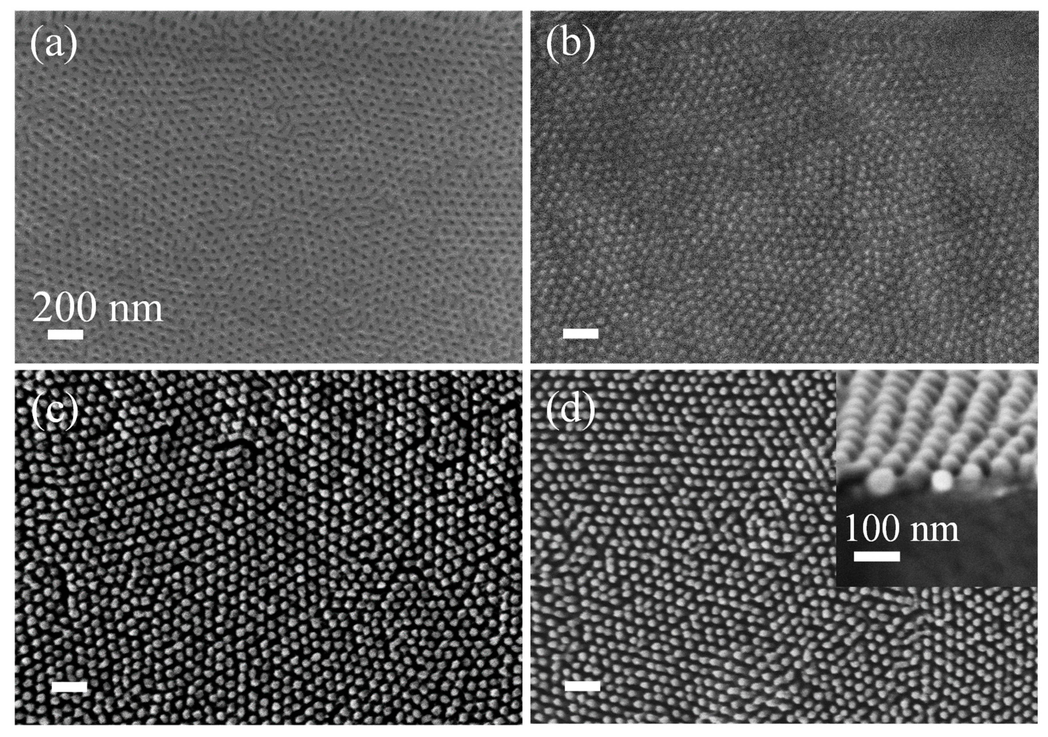
Figure 4.
SEM images of PS-b-PMMA over SiO2/MR-8 substrate: (a) self-assembled, (b) after 3 h of heat treatment at 80 °C, and (c) after eight cycles of AlOx SIS. (d) SEM image of AlOx nanocylinders on SiO2/Si substrate fabricated using the same process as (c).
Figure 4.
SEM images of PS-b-PMMA over SiO2/MR-8 substrate: (a) self-assembled, (b) after 3 h of heat treatment at 80 °C, and (c) after eight cycles of AlOx SIS. (d) SEM image of AlOx nanocylinders on SiO2/Si substrate fabricated using the same process as (c).

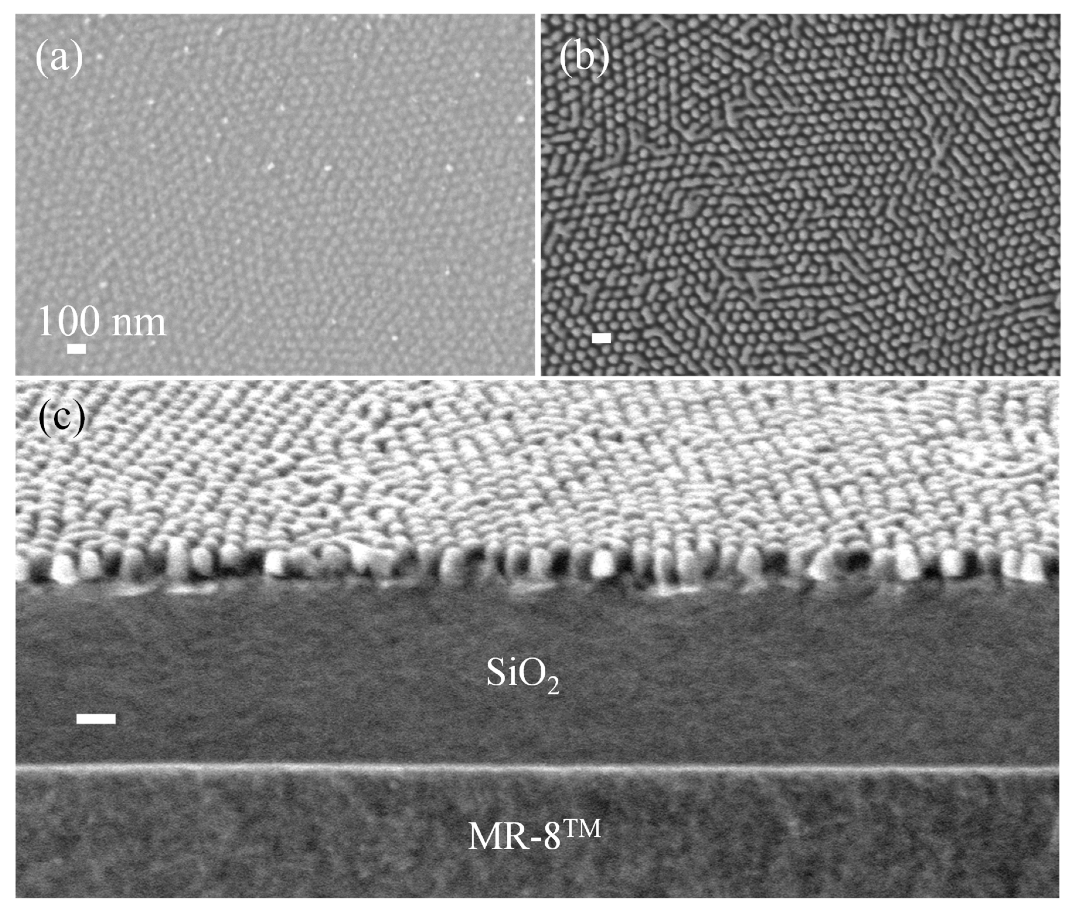
Figure 5.
SEM images of (a) PS-b-PMMA BCP layer assembled over passivated SiO2/ MR-8 substrate, (b) BCP layer after eight cycles of AlOx SIS, (c) AlOx nanocylinders after O2 plasma, and (d) AlOx/ZnO composite cylinders, templated by the layer at (a) using two cycles of AlOx SIS and six cycles of ZnO SIS, followed by O2 plasma. The inset shows a cross-sectional view of the AlOx/ZnO cylinders.

Figure 6.
SEM images of AlOx/ZnO nanocylinders over an SiO2/MR-8 polymer substrate after (a) continuous 3 min of CHF3 RIE, (b) 14 min of loop CHF3 RIE. (c) Cross-sectional view of a textured SiO2 surface generated with the process shown in (b). Scale bar is 100 nm in all images.
Figure 6.
SEM images of AlOx/ZnO nanocylinders over an SiO2/MR-8 polymer substrate after (a) continuous 3 min of CHF3 RIE, (b) 14 min of loop CHF3 RIE. (c) Cross-sectional view of a textured SiO2 surface generated with the process shown in (b). Scale bar is 100 nm in all images.

Publisher’s Note: MDPI stays neutral with regard to jurisdictional claims in published maps and institutional affiliations. |
© 2021 by the authors. Licensee MDPI, Basel, Switzerland. This article is an open access article distributed under the terms and conditions of the Creative Commons Attribution (CC BY) license (https://creativecommons.org/licenses/by/4.0/).
Share and Cite
MDPI and ACS Style
Barick, B.K.; Shomrat, N.; Green, U.; Katzman, Z.; Segal-Peretz, T. Fabrication of Nanoscale Oxide Textured Surfaces on Polymers. Polymers 2021, 13, 2209. https://0-doi-org.brum.beds.ac.uk/10.3390/polym13132209
AMA Style
Barick BK, Shomrat N, Green U, Katzman Z, Segal-Peretz T. Fabrication of Nanoscale Oxide Textured Surfaces on Polymers. Polymers. 2021; 13(13):2209. https://0-doi-org.brum.beds.ac.uk/10.3390/polym13132209
Chicago/Turabian StyleBarick, Barun K., Neta Shomrat, Uri Green, Zohar Katzman, and Tamar Segal-Peretz. 2021. "Fabrication of Nanoscale Oxide Textured Surfaces on Polymers" Polymers 13, no. 13: 2209. https://0-doi-org.brum.beds.ac.uk/10.3390/polym13132209
Note that from the first issue of 2016, this journal uses article numbers instead of page numbers. See further details here.