1. Introduction
Interest in two-dimensional (2D) materials, plasmonic and polaritonic devices increases continuously [
1,
2,
3]. It stimulates the progress of non-destructive test methods used in the infrared (IR) band and terahertz (THz) frequency range [
4,
5]. Ability to sustain high external electric fields and temperatures, chemical and mechanical robustness make the AlGaN/GaN heterostructures an attractive material for the development of high electron mobility transistors (HEMTs) as well as THz detectors, emitters, and phase modulators [
6,
7,
8,
9]. The performance of two dimensional electron gas (2DEG) and epitaxial layers in these heterostructures can be affected either by the variation of growth procedures or during the device fabrication, i.e., chemical treatment, ion plasma etching, metal electrode deposition, or surface passivation [
10,
11]. Thus, remote monitoring of high-frequency characteristics of selected heterostructure layers would allow for smarter development of novel materials and devices with optimized performance in the IR band and THz frequency range [
9,
12,
13,
14].
Here we investigate the IR and THz-frequency reflectance and transmittance of commercial AlGaN/AlN/GaN HEMT structures grown on a semi-insulating SiC substrate. Corresponding spectra were obtained using THz time-domain spectroscopy (TDS) and Fourier-transform infrared (FTIR) systems in the frequency range of 8–720 cm
−1 (0.2–22 THz and 1–90 meV) at two temperatures of 77 K and 300 K. The obtained results were analyzed numerically using the transfer matrix method, considering the heterostructure as a stack of a homogeneous media with an effective complex dielectric permittivity and the interface described by a high-frequency Drude conductivity of 2D electrons. The calculated data were fitted to the experimental spectra by varying relevant parameters of the physical model and sequentially selecting the heterostructure layers. Detailed analysis of optical characteristics of the AlN nucleation layer, unintentionally doped (UID) GaN and GaN:C buffer layers allowed modeling of the experimental spectra of the whole commercial HEMT structure including the Reststrahlen region of AlN and GaN. The transverse optical (TO) phonon damping factors of the UID GaN and GaN:C buffer layers were found to be independent from the temperature and equal to 4 and 8 cm
−1, respectively. In addition, temperature dependence of the electron effective mass in AlGaN/AlN/GaN heterostructures was observed in the THz regime. The obtained values are in agreement with previous experimental data of similar III-nitride structures but without an AlN spacer between the barrier and buffer layers [
15,
16].
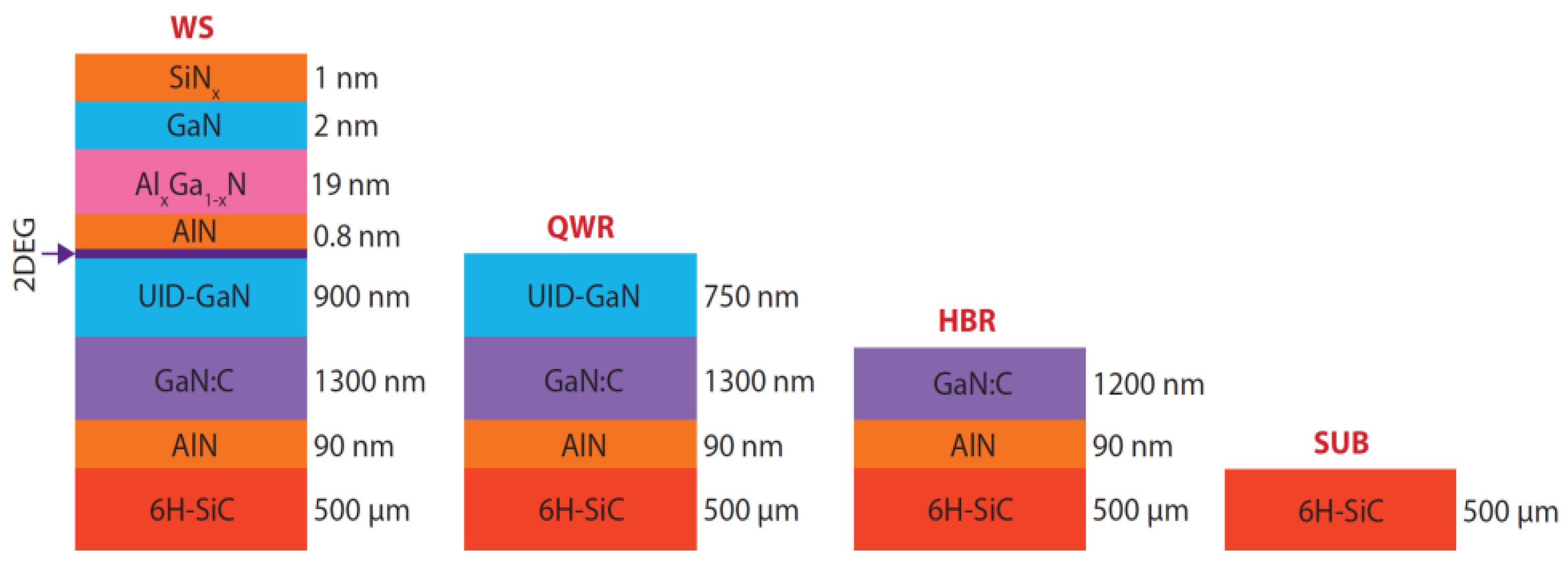
2. Heterostructure Growth and Sample Fabrication
The commercial HEMT structures for the research were provided by TopGaN Ltd., Warsaw, Poland. The heterostructures were grown using the metal organic chemical vapor deposition method on c-plane of a 500 µm thick 6H-polytype SiC substrate with a 90 nm thick AlN nucleation layer. The 1300 nm-thick high resistivity GaN:C buffer was followed by the 900 nm-thick UID GaN layer and 0.8 nm AlN spacer. On the top, a 19 nm thick Al
0.25Ga
0.75N barrier was grown capping it with 2 nm GaN and 1 nm SiN
x passivation layers. The Al mole fraction and strain states of the layers were calculated by fitting the experimental X-ray diffraction (XRD) curves with computer simulations. Sketch of the whole structure (WS) is shown in
Figure 1. The values of the 2DEG density and the electron mobility were obtained from the Hall effect measurements in a Van der Paw geometry. The results are summarized in
Table 1.
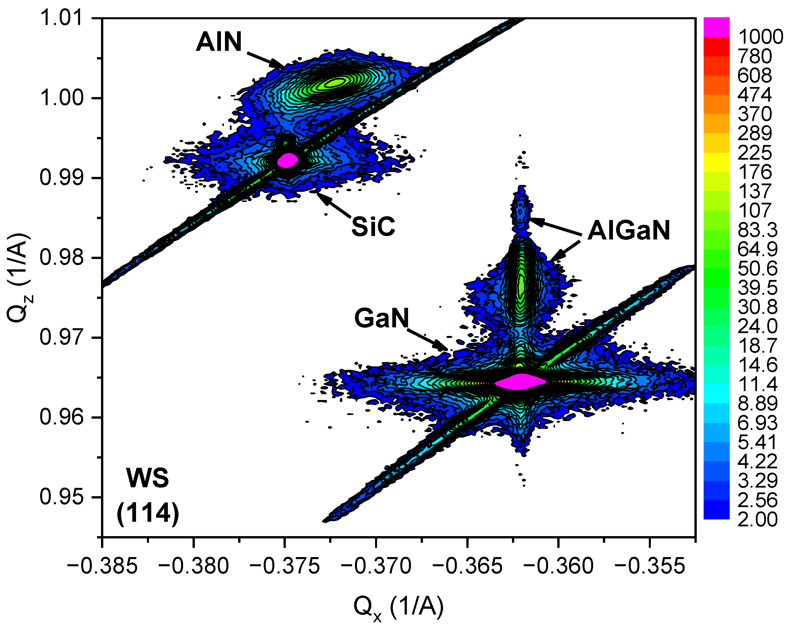
The composition and strain/relaxation state of the epilayers were observed in detail by reciprocal space mapping (RSM) employing the Malvern Panalytical, Empyrean X-ray diffractometer system. The asymmetric (105) RSM of grazing incidence and exit geometry was carried out on the WS sample. The results are shown in
Figure 2. Typical almost relaxed peaks from SiC, AlN nucleation layer, thick GaN buffer are clearly visible, while the AlGaN barrier is fully strained to GaN (shares the same x-axis coordinates of reciprocal lattice units). The rocking curve measurements revealed very good structural quality of deposited nitride layers. Namely, the full width of half maximum (FWHM) of rocking curve (RC) of symmetric (002) reflection was 0.036 deg, the FWHM RC of asymmetric (204) and (114) reflections were of 0.067 and 0.056 deg, respectively. For GaN, the lattice parameters were measured to be of
= 3.1897 and
= 0.00012, demonstrating almost relaxed layers.
The three mesas each of 4 × 4 mm
2 area but of various depth were processed on the same piece of the AlGaN/AlN/GaN HEMT structure. We used UV photolithography and chlorine-based reactive ion etching methods to this end. These mesas were purposed for an accurate investigation of the high-frequency characteristics of individual UID GaN and GaN:C buffer with AlN nucleation layers.
Figure 1 shows the sketch of layers in the processed mesas without cap and barrier layers, i.e., the quantum well removed (QWR), the half buffer removed (HBR), and only the substrate (SUB) left. The etch depth and the surface morphology of processed zones were controlled with the surface profilometer (VeecoDektak 150), scanning electron (Horriba SU70), and optical microscopes.
In addition, the selected HEMT structure sample was characterized by secondary ion mass spectroscopy (SIMS) in order to determine concentration of impurities in all epitaxial layers down to the substrate. Special surface-cleaning procedures were used before the SIMS measurement enabling a determination of the doping level well below 1017 cm−3. The averaged concentration of C atoms was found to be of about 1.5 × 1016 cm−3 and 1.2 × 1018 cm−3 in the top UID GaN and bottom GaN:C parts of the buffer layer, respectively.
3. Experimental Methods
A FTIR spectrometer Bruker Vertex 80v operating in a rapid-scan mode, vacuumed to 4 mbar and equipped with a globar as a source of radiation and a Mylar or KBr beam-splitter, was used to study the transmittance of the samples under normal illumination. For the measurements at various temperatures, the samples were mounted on a cold finger of a closed cycle cryostat above a copper holder with a 3 mm diameter pinhole. The intensities of initial and transmitted through the sample beams were measured by a DLaTGS-FIR pyroelectric detector in the spectral range of 70–400 cm−1 (8.7–50 meV). A spectral resolution of 4 cm−1 (0.5 meV) was chosen to suppress the Fabry–Pérot (F−P) oscillations due to multiple radiation reflections inside the SiC substrate. Measurements were carried out for the samples WS, QWR, SUB and empty sample holder. Combining these four measurements, we determined the transmittance of the whole HEMT structure and found the characteristic spectra of 2DEG and GaN buffer layers.
Additionally, the reflectance of the samples was studied by the vacuumed FTIR spectrometer (Bruker V70) at room temperature in the spectral range of 380–720 cm−1 (47–90 meV). The angle of incidence was of about 11 degrees. A thick gold film was used for the reference measurements. The intensity of the IR radiation was measured by a DLaTGS pyroelectric detector. The features related to TO phonons in the UID GaN, GaN:C buffer and AlN nucleation layers were identified in the reflectance spectra, revealing the values of phonon damping factors. The correlation between magnitude of the damping factors and crystal quality of the GaN epitaxial layers was investigated in detail.
A THz TDS spectrometer (T-SPEC 800) was employed to measure the transmittance in the frequency range of 8–80 cm
−1 (1–10 meV). Results were obtained at two temperatures provided by liquid nitrogen cryostat [
9]. The artifacts due to water vapor absorption were minimized by purging the TDS system with dry nitrogen. The signal was recorded over a time window of approximately 10 ps which provided spectral resolution of 3.3 cm
−1 avoiding unwanted F−P oscillations.
4. Modelling of Reflectance and Transmittance Spectra
The reflectance and transmittance spectra of the samples were modelled using the transfer matrix method [
17]. We considered the normal incidence of electromagnetic radiation considering the following layers: (0) vacuum, (1) barrier, (2) top part of the buffer (UID GaN), (3) bottom part of the buffer (GaN:C), (4) nucleation layer, (5) substrate and (6) vacuum. Layer sketches are presented in the insets of respective
Figure 3 and Figure 6.
Radiation propagation through the
i-th layer (
i = 1–5) is described by the propagation matrix
Pi:
where the phase shift
of the electric field vector is given by
and are the complex refractive index and thickness of the layer, respectively. Complex dielectric permittivity εi of the i-th layer is related to by the Fresnel equation: .
For a conducting interface (
i+1)/
i the transfer matrix
was written as [
18]
where
is the surface conductivity of the interface. For a non-conducting interface, Equation (3) can be used with
= 0.
The transfer matrix
M for the whole structure is related to above matrices as
and the transmittance
T and reflectance
R can be found by
and
respectively.
Generally, the transmittance and reflectance spectra simulated using Equations (5) and (6) demonstrate the short-period oscillations due to multiple passes of radiation inside a thick substrate. Such F–P oscillations are clearly seen on experimental spectra in the case of sufficiently high resolution [
8,
9,
19]. In our experiments, we used a reduced spectral resolution that eliminated F–P oscillations. To perform corresponding transformation of the simulated spectra we considered the substrate (layer 5) as an “incoherent layer” [
17]. Namely, Equations (5) and (6) were modified as:
and
with the following changes of the Equations (1) and (4):
and
-respectively. In such a way, we average the total transmittance and reflectance over all values of a phase δ inside layer 5. Such calculation is appropriate when the double substrate thickness exceeds the coherent wavelength inside a material defined as
, here
is the spectral resolution in wavenumbers. It should be noted that this condition was fulfilled over the entire spectrum range of interest.
In our model, the barrier (layer 1) represented a stack of four upper layers in a real HEMT structure. The total thickness of the stack
= 22.8 nm was much less than the wavelength of THz radiation, enabling us to consider the stack as homogeneous media with an effective complex dielectric permittivity. Its magnitude
ε1 is close to the dielectric constant of Al
0.25Ga
0.75N which is described as
Spectral dependences of AlN and GaN dielectric permittivities on the right side of Equation (11) are evaluated in one-phonon-resonance approximation:
where
and
are the low- and high-frequency dielectric constants, respectively,
and
γ are the oscillation frequency and the damping factor of TO phonons, respectively. The numerical values of these parameters were taken from literature [
19,
20,
21] and found by fitting experimental data and are summarized in
Table 2.
The UID GaN (layer 2) and the high resistivity GaN:C buffer (layer 3) were described by Equations (1), (2) and (12). It is known that the lattice quality of the bottom part of a GaN buffer can be rather low due to lattice mismatch against the substrate material which results in a variation of the phonon damping factor
γ along the growth direction of the structure [
22]. For this reason, we introduced different damping factors
and
for the layers 2 and 3, respectively. The AlN nucleation layer was described by Equations (1), (2) and (12) using the values of
,
and
listed in
Table 2. The damping factor of this layer
was used as fitting parameter.
The elements of the propagation matrix
describing the substrate were calculated using the experimental data on a complex refractive index of 6H-SiC published recently in Refs. [
23,
24].
The heterostructure under investigation includes one conducting interface only. This is the barrier/buffer interface. Its transfer matrix
is determined by the conductivity of 2DEG at the interface which was simulated using the Drude model:
where
Ns is 2DEG concentration,
is effective mass of 2D electrons and
is their relaxation time determined by the mobility:
.
The transmittance and reflectance of the samples QWR, HBR and SUB obtained by FTIR spectroscopy were calculated in a similar way. For these samples the transfer matrices , and were used, respectively.
It should be noted that the modelling algorithm of the THz spectra obtained with THz TDS spectrometer was slightly different from above. It was used for a short time window of 10 ps for measurement of single pass THz pulse characteristics [
9]. Consequently, the optical transmittance of the whole structure can be written as
where the optical transmittance
of all the epitaxial layers were simulated using their total transfer matrix,
and Equation (5) replacing
with
. In Equation (14),
and
denote the absorption coefficient of the substrate and the reflection coefficient of the substrate/vacuum interface, respectively.
5. Results and Discussion
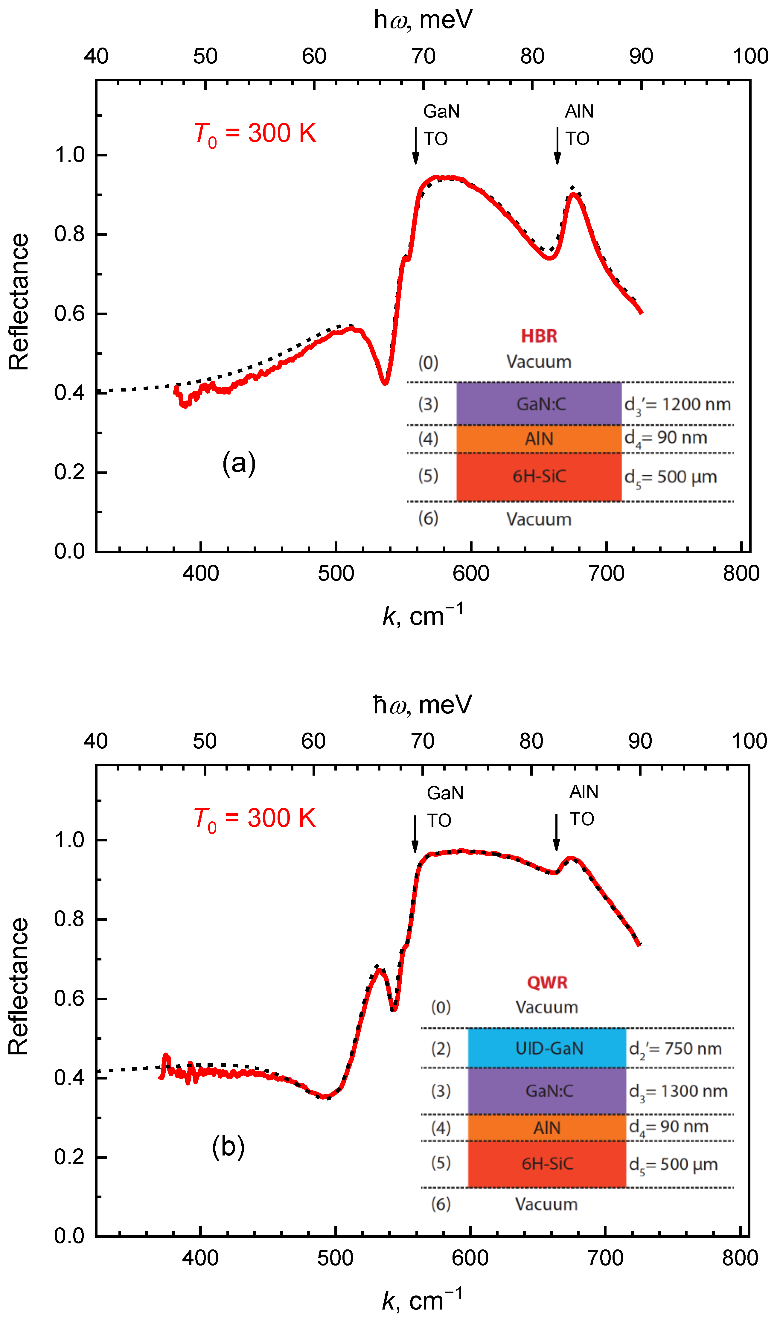
At first we analyzed the reflectance spectra of the samples QWR and HBR. The selected spectral range of 380–720 cm−1 overlaps with the Reststrahlen region of AlN and GaN providing for the access of resonant features of TO phonons in UID GaN, GaN:C buffer and AlN nucleation layers of the heterostructure. In particular, the shape of the feature is very sensitive to the variations of the layer thickness and the phonon damping factor of each layer, namely, , and . The latter values were correlated with the crystal quality of the epitaxial layer. The TO phonon damping factors were used as variable parameters fitting simulated data to the experimental reflectance spectra.
The reflectance of the sample HBR at room temperature is shown in
Figure 3a. The spectrum was modelled assuming that the amplitude of the reflectance peak in the vicinity of TO phonon resonance of AlN layer (at 675 cm
−1) is controlled by the damping factor
while the interference pattern in the wavenumber range of 450–555 cm
−1 is defined by the
and
parameter values of the GaN:C layer possessing the TO phonon resonance at 559 cm
−1. There is a strong dispersion here of the refractive index which results in an irregular interference pattern due to multiple radiation reflections inside the GaN:C layer. Namely, one can see the interference maxima at 513 and 552 cm
−1 and the interference minimum between them at 535 cm
−1. By fitting the simulated results to the experimental spectrum (see
Figure 3a), the parameters of the AlN nucleation layer and the GaN:C buffer layer were obtained:
= 4.02 cm
−1,
1200 nm and
= 8.0 cm
−1. It is important to note that the obtained value of the phonon damping factor of 8.0 cm
−1 for the GaN buffer is up to 2.5 times smaller than that found in [
22], for a similar buffer layer but grown on sapphire substrate and without the usage of an AlN nucleation layer. Therefore, our results demonstrate that the use of an optimal nucleation layer for the growth of commercial HEMT structures on the SiC substrate is beneficial as the crystal quality of the upper GaN layer improves significantly. Moreover, a considerable improvement of low-frequency electrical performance as well as a weaker quenching of reduced magnitude THz electroluminescence from shallow impurities remaining in a commercial HEMT structures were demonstrated over the AlGaN/GaN/sapphire platform [
10,
25]. The increase in the value of phonon damping factor in the bottom part of the GaN buffer was also observed and associated with an extrinsic phonon scattering at the lattice imperfections resulting from lattice mismatch as an effect of a foreign substrate [
22].
The parameters of the UID GaN layer (layer 2 in the considered model) were determined from the experimental reflectance of the QWR sample. The results are shown in
Figure 3b. The spectrum demonstrates an inversed interference pattern in the range of 450–555 cm
−1, namely, there are two interference minima at 493 and 550 cm
−1 and one maximum between them at 532 cm
−1. This transformation of the interference pattern is associated with the increase of total thickness of GaN layers by a factor of 1.7 in comparison to that in the HBR sample. By fitting the simulation data to the experimental spectrum (see (
Figure 3b), the thickness and phonon damping factor for the UID GaN layer was found to be of
750 nm and
= 4.0 cm
−1, respectively. Note that the value of the TO phonon damping factor indicates the GaN epitaxial layers with quality similar to those grown on native and foreign substrates [
21,
22].
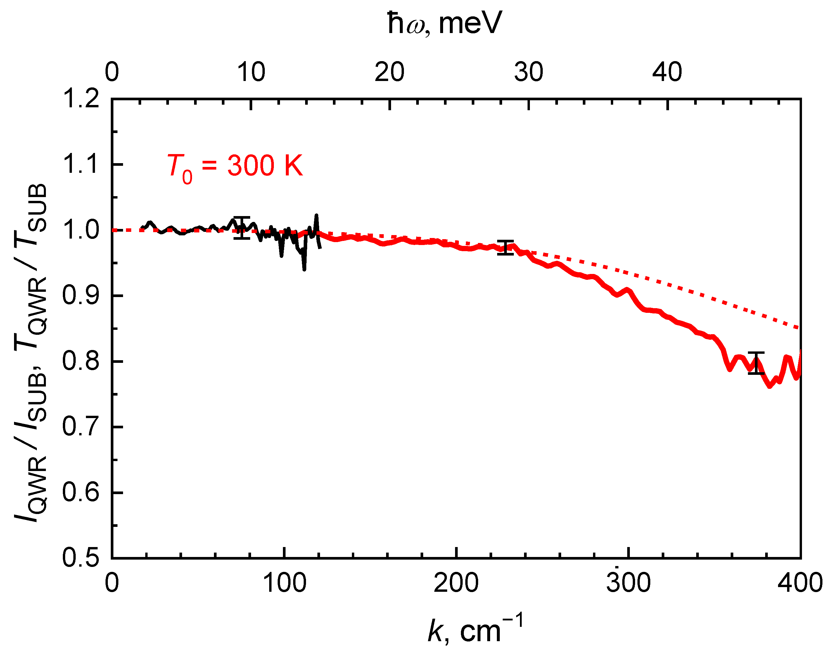
Next, we investigated the relative spectrum of UID GaN, GaN:C buffer and AlN nucleation layers measuring the intensities
IQWR and
ISUB at the output of the QWR and SUB samples, respectively. The
IQWR/
ISUB ratio spectrum is shown in
Figure 4. It was considered as a characteristic transmittance of the stack of all three layers. The theoretical spectrum was also found modeling the ratio of
TQWR/
TSUB, here
TQWR is the transmittance of the QWR sample calculated using the best-fit parameters modeling the reflectance of the HBR and QWR samples. The model for the transmittance
TSUB of the 6H-SiC substrate (sample SUB) was described in
Section 4.
As it is seen from
Figure 4, the simulated relative spectrum of the stack of UID GaN, GaN:C buffer and AlN nucleation layers is in a good agreement with the experimental one at wavenumbers
k < 250 cm
−1, but at higher wavenumbers, there is a noticeable discrepancy. Namely, the experimental relative spectrum demonstrates a negative deviation with values up to about 7% at
k = 400 cm
−1. Similar negative deviation (of about 6% at
k = 400 cm
−1) can be detected for the experimental reflectance spectrum of the QWR sample in the spectral range of 380–450 cm
−1 (see also
Figure 3b). Obviously, the simultaneous signal attenuation in both spectra at the same spectral range can be associated with scattering of incident radiation that was not considered in the model used. It might be that the radiation was scattered by the rougher surfaces of the QWR sample caused by reactive ion etching.
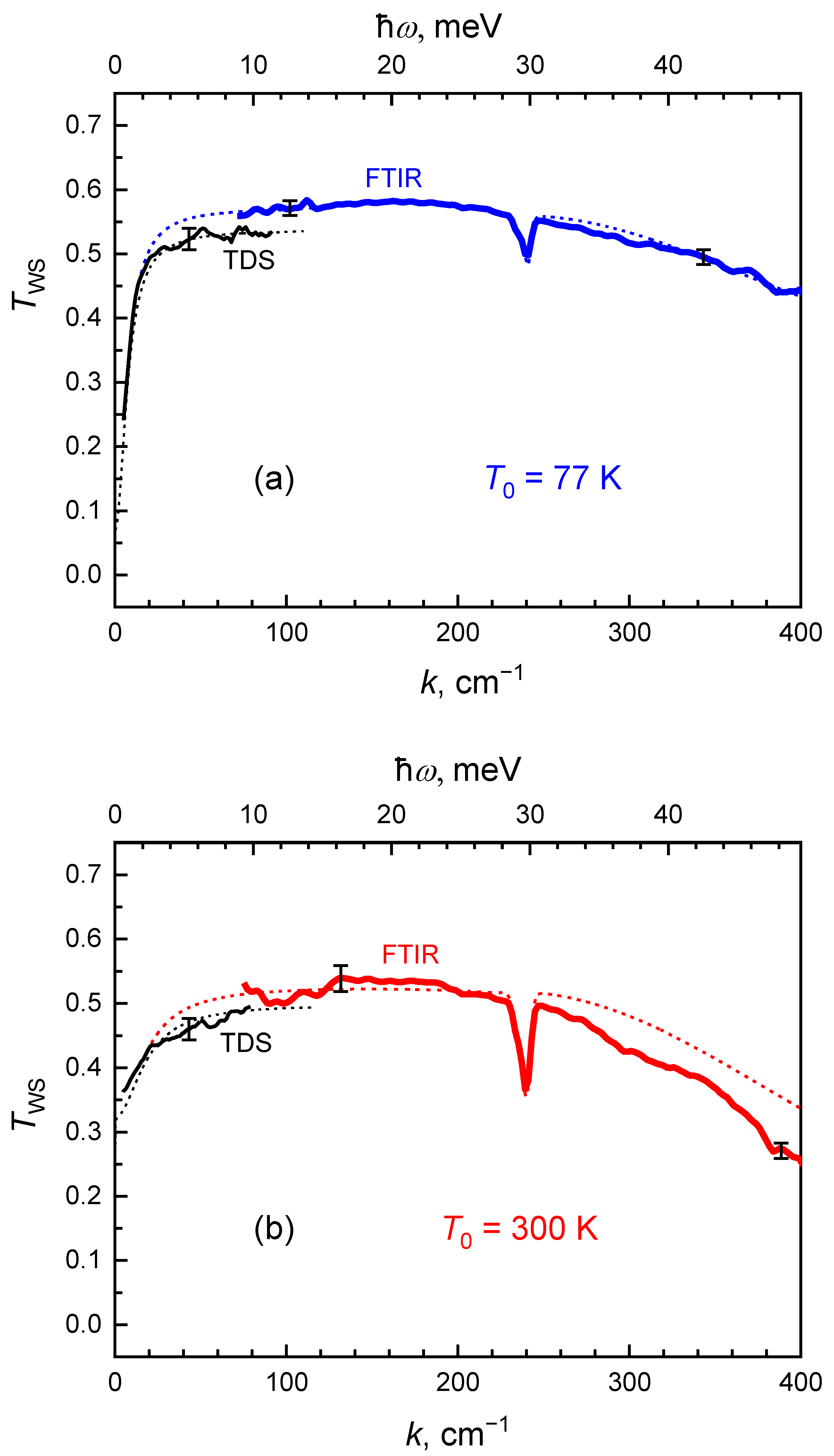
The transmittance spectra of the whole heterostructure obtained by the FTIR method at two temperatures are shown in
Figure 5 by thick solid lines. A significant peculiarity of both spectra is a sharp dip around wavenumber of 240 cm
−1. The dip is not associated with the epilayers of the heterostructure: it is due to folded transverse acoustic phonon modes in the 6H-SiC substrate [
23,
24]. The spectra obtained by the TDS method (thin solid lines) demonstrate smaller transmittance values in comparison to the FTIR data. In particular, the transmittance at wavenumber of 80 cm
−1 is smaller by about 5%. The reduction was associated with a single pass of THz pulse through the sample due to a rather short time window taken for analysis of TDS measurements in order to avoid the appearance of F–P oscillations in the spectra.
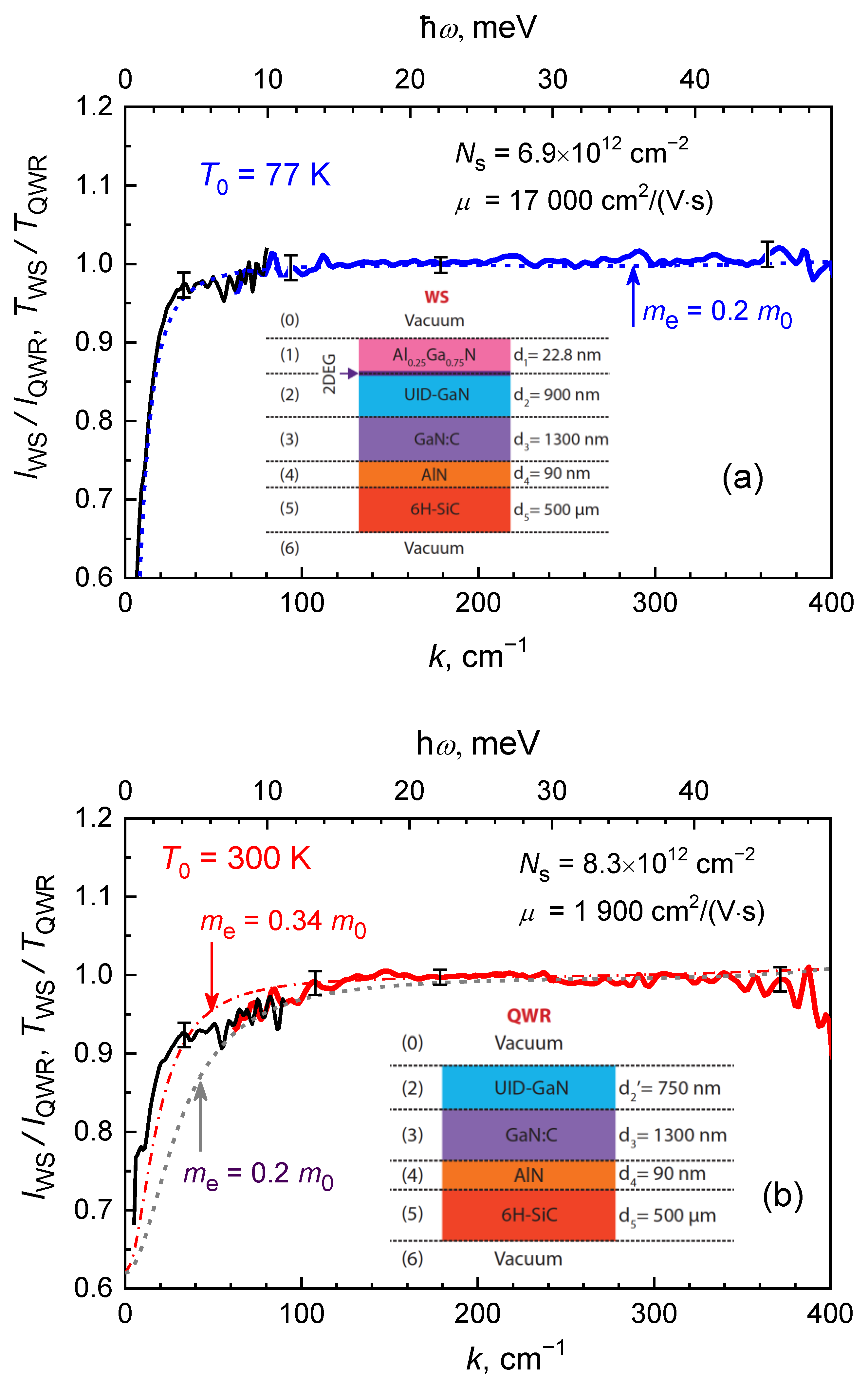
THz performance of 2DEG was experimentally examined comparing the intensities
IWS and
IQWR recorded for the WS and QWR samples, respectively. The
IWS/
IQWR ratio spectrum is shown in
Figure 6. It was attributed to the high-frequency characteristic of 2DEG layer as the radiation absorption in all epilayers above the QW with a total thickness of 22.8 nm was found to be negligibly small in the whole spectrum under consideration. The simulations demonstrated that the change of the
IWS/
IQWR ratio should not exceed 0.1% going from the FTIR method to the TDS method and this is much smaller than the experimental accuracy of both methods used. Although, a single pass and multi pass transmission through the substrate result in different absolute values obtained by the two methods, it proportionally modifies both intensities in the numerator and in the denominator of the ratio
IWS/
IQWR. Similarly, the I
QWR/
ISUB ratio is convenient for the characterization of the stack of UID GaN, GaN:C buffer and AlN nucleation layers (see also
Figure 4).
Modelled relative spectrum of
TWS/
TQWR ratio was also calculated. The results are shown in
Figure 6. Simulation was performed with the help of Equation (13) using a common value of the electron effective mass
[
26] and corresponding 2DEG parameters measured for our HEMT structures in the Hall experiment (
Table 1). At the temperature of 77 K, the theoretical simulations are in a good agreement with experimental results (
Figure 6a). The main feature in the transmittance spectrum is the monotonic amplitude increase with the increase of incident photon energy visible up to 15 meV. This steep shoulder is a fingerprint of free carrier absorption due to high-frequency Drude conductivity of 2DEG in AlGaN/AlN/GaN HEMT structures.
We noticed that at room temperature, the numerical modelling suggested a significantly flat Drude part of the transmittance spectrum in comparison to that measured in the experiment (see dashed and solid lines in
Figure 5b). However, the numerical modelling fitted much better to the experiment if the effective electron mass
[
15] was used (compare dash-dot and solid lines in
Figure 6b). The renormalization of the electron effective mass starting from the temperature of 134 K was also found in AlGaN/GaN heterostructures but without AlN spacer conducting the optical Hall effect experiments with free 2D electrons [
16] and the THz TDS of 2D plasmons [
15]. These two independent works revealed that the electron effective mass changes from
at 80 K to
at 300 K and to
at 294 K, respectively.
It is worth noting that the use of calibration samples would allow for further development of the IR-THz spectroscopy method for use as a non-destructive characterization tool of the UID GaN, GaN:C buffer, AlN nucleation and 2DEG layers of different commercial AlGaN/GaN HEMT structures.
6. Conclusions
The infrared-terahertz spectroscopy method has been developed for the investigation of optical performance of 2DEG and GaN:C buffer layers in the AlGaN/AlN/GaN heterostructures grown on SiC substrate. The high-frequency Drude conductivity of the 2DEG layer and the single-phonon-resonance dielectric permittivity of the barrier, buffer and nucleation layers were taken into consideration in the transfer matrix method in order to describe the experimental data.
Attenuation of the transmitted signals in the long-wavelength spectrum part at temperature of 77 K was associated with high-frequency Drude conductivity of 2DEG. However, at room temperature, the simulation predicted a noticeably wider attenuation band than that observed in the experiment. The discrepancy between theory and experiment was eliminated assuming a 1.5-fold increase in the electron effective mass with the increase of temperature.
Transmittance and reflectance of samples with sequentially removed UID GaN, GaN:C buffer and AlN nucleation layers by reactive removing allowed the investigation of the TO phonon damping factor in the frequency range of 380–720 cm−1. It was demonstrated that the presence of a proper AlN nucleation layer on SiC substrate allowed the reduction of the phonon damping factor of GaN:C buffer by a factor of 2.5 in comparison to the buffers which were grown directly on Al2O3 substrate. Therefore, the deposition of the nucleation layer significantly improves the crystal quality of epitaxial layers by growing them on foreign substrates.
This work opens the way for the development of non-destructive test methods based on terahertz and infrared spectroscopies of high-frequency performance of epitaxial GaN and 2DEG layers in the commercial AlGaN/GaN high-electron mobility transistor structures.


 ,
, 


