Article

Effects in the Optical and Structural Properties Caused by Mg or Zn Doping of GaN Films Grown via Radio-Frequency Magnetron Sputtering Using Laboratory-Prepared Targets

by
Erick Gastellóu
1,*,
Godofredo García
2,
Ana María Herrera
3,
Crisoforo Morales
2,
Rafael García
4,
Gustavo Alonso Hirata
5,
Enrique Rosendo
2,
José Alberto Luna
2,
Mario Robles
1,
Jorge Alberto Rodríguez
1 and
Yani Dallane Ramírez
6
1
División de Sistemas Automotrices, Universidad Tecnológica de Puebla (UTP), Puebla 72300, Mexico
2
Centro de Investigación en Dispositivos Semiconductores, Benemérita Universidad Autónoma de Puebla (BUAP), Puebla 72570, Mexico
3
Ingeniería en Software, Universidad Politécnica de Amozoc (UPAM), Amozoc 72980, Mexico
4
Departamento de Investigación en Física, Universidad de Sonora, Hermosillo 83190, Mexico
5
Centro de Nanociencias y Nanotecnología, Universidad Nacional Autónoma de México (UNAM), Ensenada 22800, Mexico
6
División de Ingeniería Ambiental, Universidad Tecnológica de Puebla (UTP), Puebla 72300, Mexico
*
Author to whom correspondence should be addressed.
Submission received: 16 June 2021 / Revised: 18 July 2021 / Accepted: 18 July 2021 / Published: 29 July 2021
(This article belongs to the Special Issue III-V Semiconductor Nanostructures)

Abstract

:
GaN films doped with Mg or Zn were obtained via radio-frequency magnetron sputtering on silicon substrates at room temperature and used laboratory-prepared targets with Mg-doped or Zn-doped GaN powders. X-ray diffraction patterns showed broadening peaks, which could have been related to the appearance of nano-crystallites with an average of 7 nm. Scanning electron microscopy and transmission electron microscopy showed good adherence to silicon non-native substrate, as well as homogeneity, with a grain size average of 0.14 µm, and 0.16 µm for the GaN films doped with Zn or Mg, respectively. X-ray photo-electron spectroscopy demonstrated the presence of a very small amount of magnesium (2.10 mol%), and zinc (1.15 mol%) with binding energies of 1303.18, and 1024.76 eV, respectively. Photoluminescence spectrum for the Zn-doped GaN films had an emission range from 2.89 to 3.0 eV (429.23–413.50 nm), while Mg-doped GaN films had an energy emission in a blue-violet band with a range from 2.80 to 3.16 eV (443.03–392.56 nm). Raman spectra showed the classical vibration modes A1(TO), E1(TO), and E2(High) for the hexagonal structure of GaN.

Graphical Abstract

1. Introduction

In the last two decades, the III-Nitride semiconductor materials have become more apparent due to their applications in optoelectronics devices, which can be tuned to different wavelengths, ranging from green to ultraviolet emission. GaN belongs to the III-Nitride group; this is a material with great potential for the present and future of the electronics industry, due to its optical, structural, and electrical properties. Gallium nitride has applications in solar cells, microwave devices, LED screens, and high-electron-mobility transistors (HEMTs) [1,2,3]. However, the principal application of GaN is the conservation of electrical energy through the replacement of incandescent light bulbs with LED technology bulbs. Recently, the GaN has also been used in applications for nuclear radiation detectors, biosensors, and nuclear batteries with high energy density/long lifetime, as well as small-scaled fabrication of pacemakers. In this way, GaN is helping to save lives [4,5,6,7,8,9].
The GaN crystallizes in the hexagonal structure, with a band gap energy of Eg = 3.4 eV. However, it should be considered that GaN wafers are very expensive, due to the methods used for the production of ingots (ammonothermal growth, and hydride vapor phase epitaxy). Thus, the GaN can be obtained via films grown on non-native substrates such as Si, SiC, and GaAs. The growth methods mostly used to obtain GaN films are metalorganic chemical vapor deposition (MOCVD) and molecular-beam epitaxy (MBE). On the other hand, obtaining this p-type GaN has been very important in device development. However, MOCVD and MBE need additional compounds to dope the GaN with Mg or Zn, which are the most common dopant elements to obtain the p-type GaN. MOCVD requires metalorganic compounds such as biscyclopentadienylmagnesium (Cp2Mg) or diethylzinc ((C2H5)2Zn), followed by the activation technique of atoms’ “low-energy electron beam irradiation (LEEBI)”, which is a process applied at the laboratory level with acceleration voltages of the incident electrons at 10 kV. Therefore, this is not an adequate process for standard applications [10,11,12]. Molecular-beam epitaxy generally uses a solid source of Mg or Zn atoms during the growth process of the material [13,14,15].
Recently, radio-frequency magnetron sputtering has been used as another option for obtaining GaN films, which could be applied as buffer layers to reduce the difference in the thermal expansion coefficients between substrate and GaN. However, this technique might require the availability of GaN powders with high purity and a single-phase for use as a raw material in the targets’ production. Additionally, GaN powders can be doped with Mg or Zn during the synthesis process [16,17,18,19,20,21]. This work presents the effects of doping with Mg or Zn in the structural, and the luminescent properties of GaN films, which were grown via radio-frequency magnetron sputtering, using laboratory-prepared targets with Mg-doped or Zn-doped GaN powders. These powders were reported by our research team in previous works [16,17,19]. The obtained films might be applied as buffer layers in III-Nitride biosensors, pacemakers, and micro-electromechanical systems (MEMS). It is also important to mention that GaN films doped with Mg or Zn were obtained for the first time using targets prepared with this process. GaN films doped with Mg or Zn showed good adherence to the non-native substrate (silicon), whose structural characteristics were obtained by X-ray diffraction (XRD), and transmission electron microscopy (TEM). Surface morphology was obtained by scanning electron microscopy (SEM), while its elemental analysis was obtained via energy dispersive spectroscopy (EDS). Mg or Zn incorporation in the GaN films was demonstrated by X-ray photoelectron spectroscopy (XPS). The film thickness was found using profilometry, and its resistivity via the four-point probe measurement method. Optical analysis was carried out using Raman spectroscopy and photoluminescence (PL).

2. Materials and Methods

GaN films doped with Mg or Zn were obtained via radio-frequency magnetron sputtering over silicon substrates at room temperature (the substrate was not heated), using laboratory-prepared targets with Mg-doped or Zn-doped GaN powders.

2.1. Material Synthesis for the Laboratory-Prepared Targets

The laboratory-prepared targets were elaborated using Mg-doped or Zn-doped GaN powders, whose synthesis processes were reported by our research group in previous works (Gastellóu et al. [16,17,19]). A brief description of the process used to obtain Mg- or Zn-doped GaN powders is provided. To synthesize the Zn-doped GaN powders, 7.477 g (107.20 mmol) of metallic gallium (99.999% pure), and 0.075 g (1.15 mmol) of metallic zinc, which was approximately 1% in the mixture, were used as reagents. The synthesis of Mg-doped GaN powders, 5.874 g (84.24 mmol) of metallic gallium, and 0.059 g (2.44 mmol) of metallic magnesium, which was also approximately 1% in the incorporation, were used as reagents. Additionally, anhydrous ammonia (NH3) was used as the source of nitrogen atoms in both processes. The processes begin by placing the metallic gallium and metallic zinc (or metallic magnesium) in an alumina boat, which was preheated on a hot plate at 200 °C and two hours of manual agitation was performed. After this time, the obtained metallic liquid solution was placed inside a CVD furnace, which was purged with an N2 flow of 150 sccm (processed at room temperature), to reduce the residual oxygen. Then, an N2 flow of 50 sccm was opened, and the temperature was increased until reaching 20 °C above the fusion temperature of the doping element, which was carried out to ensure the diffusion of the Zn atoms (or Mg atoms) in the gallium by supersaturation of the liquid solution. Table 1 presents the fusion temperature of the doping elements. Once the homogenization temperature was stabilized (Table 1), the liquid solution was homogenized for 14 h in an N2 flow of 50 sccm. Then, the N2 flow was closed, and an NH3 flow of 150 sccm was opened to make the nitridation process; the temperature was then increased to 1000 °C, where the liquid solution remained for two hours. When this time elapsed, the temperature was decreased to 600 °C, where the NH3 flow was closed, and the N2 flow of 50 sccm was opened again, while the temperature continued decreasing until it reached the room temperature, ending the process. Thus, using this process, 8.34 g (164.49 mmol) of Zn-doped GaN powders were synthesized, with a nitrogen incorporation of 0.786 g (56.14 mmol) after the nitridation. Additionally, 6.34 g (115.65 mmol) of Mg-doped GaN powders were also synthesized, with a nitrogen incorporation of 0.405 g (28.97 mmol) after the nitridation process.

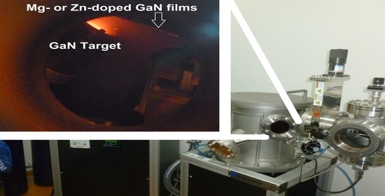
2.2. Mg- or Zn-Doped GaN Films

Once the Mg- or Zn-doped GaN powders were obtained, a tableting process was used to prepare the targets for the films’ deposition. First, an agate mortar was used to finely grind the powders and were then lubricated with 0.5 mL of methanol to obtain a mixture. Afterward, the mixture was placed in a Blackhawk SP25B powder press to obtain the target (with a pressure of 10 ton/cm2). When the powders were compacted, the target was removed from the press to be individually sintered. The targets were sintered inside a conventional CVD furnace using an N2 flow (150 sccm) at 900 °C for one hour to reduce the oxygen non-intentional impurities introduced with the methanol. The above process was repeated until the targets had the required hardness for the deposition by radio-frequency magnetron sputtering. Mg- or Zn-doped GaN films were deposited via radio-frequency magnetron sputtering at room temperature using an Intercovamex Sputtering System V1, (with a target size of 25.4 mm in diameter, and 5 mm in thick). A separation distance between the substrate and the target of 40 mm was applied. A chamber vacuum attained a pressure of 2 × 10⁻⁶ Torr before the layer growth. An N2 flow was used during sputtering, as well as a RF power of 50 W and a gas pressure of 25 × 10−3 Torr were kept during the sputtering deposition. It also required a longer deposition time of 8 h to grow a thick layer [20,22]. Additionally, silicon (100) substrates were used to remove organic residues, along with the conventional cleaning of solvents and solutions. A diagram of this process of obtaining the Mg- or Zn-doped GaN films is shown in Figure 1a, while Figure 1b shows the targets prepared using Mg-doped, or Zn-doped GaN powders (Gastellóu et al. [17,19]).

2.3. Characterizations

Mg- or Zn-doped GaN films were characterized by X-ray diffraction (XRD) measurements using a Bruker AXS D8 Discover Diffractometer at room temperature, equipped with a wavelength (Cu Kα) of 1.5406 Å. The XRD patterns were obtained in a range from 25° to 60°, with step-size and step-time of 0.02° and 1 s, respectively. The X-ray tube operation conditions were 40 kV and 40 mA. The surface morphology and elemental analysis (SEM/EDS) of the Mg- or Zn-doped GaN films were obtained using a JEOL JIB-4500 (SEM+FIB). The profilometry was made using a Dektak 150 Surface Profiler. Photoluminescence spectra (PL) were measured at room temperature with an excitation wavelength of 243 nm and a 310 nm filter using a fluorescence spectrophotometer Hitachi F-7000 FL with a 150 W xenon lamp. The Raman-scattering characterizations of the Mg- or Zn-doped GaN films were obtained using a Horiba Jobin Yvon HR-800 Micro Raman spectrophotometer. X-ray photoelectron spectroscopy (XPS) measurements were taken with an Escalab 250Xi Brochure, using an energy range from 0 to 1400 eV. Four-point probe measurements were carried out using a Lucas Signatone QuadPro Resistivity System.

3. Results and Discussion

3.1. Structural Analysis

Figure 2 shows the main peaks in X-ray diffraction patterns for the Mg-doped GaN films (Figure 2a), and Zn-doped GaN films (Figure 2b), as well as the ICDD card 00-050-0792 for hexagonal GaN (Figure 2c), which was used to compare the different X-ray diffraction patterns. The peaks observed in Figure 2 were indexed in the ICDD card 00-050-0792 for GaN. The a peak was located in the plane orientation (100), b had a localization at (002), c had the highest intensity at (101), d peak was located at (102), while e peak was located at (110). The lattice constants for the hexagonal structure were a = 3.18 Å and c = 5.18 Å, with a ratio c/a = 1.62. The FWHM average measurements for the c peak (101) of the X-ray diffraction patterns of Figure 2, had a value of 1.15°. The c peak broadening of the X-ray diffraction patterns could be produced for two reasons. First, this deposition technique does not produce good crystalline quality in the layers at room temperature; however, when the substrate is heated, the crystalline quality in the films could get better [22]. Second, the presence of nano-crystallites hinders the crystalline quality [16]. On the other hand, Figure 2a,b does not show a significant difference between their diffraction angles. This similarity might show that the incorporation of the magnesium or zinc atoms into the GaN lattice did not affect its crystalline structure, due to the approximate atomic radius of the dopant elements [23]. The percentage similarity of Mg and Zn compared to gallium is 88% and 92%, respectively. Using the ICDD PDF-4+ 2018 software and the Debye–Scherrer equation, the crystal size was computed, finding an average of 7 nm for all GaN films. Figure 2a,b, showed small peaks in GaN in the (102), and (110) planes, which could be related to growth temperature, a poor nitrogen incorporation, and the introduction of probable oxygen non-intentional impurities into the crystalline lattice during the deposition by sputtering.

3.2. Electron Microscopy, Profilometry and Resistivity

Figure 3 shows the superficial morphology for the Zn-doped GaN films (Figure 3a), and Mg-doped GaN films (Figure 3b). SEM micrographs of the grown films by radio-frequency magnetron sputtering demonstrated good adherence to the substrate, as well as homogeneity. Figure 3a showed an irregular grain surface with a grain size average of 0.14 µm. Figure 3b also demonstrated an irregular grain surface with a grain size average of 0.16 µm, where the irregular grains could be formed by a crystallite agglomerate with a size average of 7 nm, as can be calculated from the XRD analysis using the ICDD PDF-4- 2018 software and the Debye–Scherrer equation. Mg- or Zn-doped GaN films, grown by sputtering using laboratory-prepared targets of Mg- and Zn-doped GaN powders, had a better adherence and homogeneity compared to grown films obtained via nitridation of GaAs substrates or MOCVD [18]. EDS elemental analysis corresponding to Figure 3a,b is shown in Figure 3c,d, respectively. These spectra only demonstrated an elemental contribution of gallium, nitrogen, and a small elemental contribution of oxygen in the Mg- or Zn-doped GaN films. It is important to mention that the residual oxygen’s non-intentional impurity might be related to the hysteresis effect, which can occur in the early stages of the sputtering deposition due to system instability. This residual oxygen could affect the optical properties of the GaN films, producing emission peaks in the red luminescence (RL). EDS spectra did not show the presence of the incorporation of magnesium or zinc, which could be due to its small atomic percentage (1.0 mol %), compared to other elements. Additionally, the overall accuracy of the equipment used was approximately 1 weight percent (wt%) with a sensitivity of approximately 0.1 weight percent (wt%) [17,19]. EDS elemental analysis does not show the contributions of other impurity atoms such as carbon, or silicon belonging to the substrate.
Figure 4 shows the X-ray photo-electron spectroscopy (XPS) of the Mg- or Zn-doped GaN films. Both samples showed similar behavior in the peaks for high energies of Ga 2P3/2 and Ga 2P1/2 with respective values of 1117.75 and 1144.61 eV, which has a difference of 1.35, and 1.41 eV for the L2, and L3 levels of the element in its natural form, respectively (Figure 4a). The atomic percentage for Ga 2P was approximately 51.7%. Additionally, the energy peak related to N 1s in both samples was obtained at 398.43 eV for the K level (Figure 4b), with an atomic percentage of 31.1%. This characterization technique showed the presence of a very small amount of magnesium (2.10 mol%), and zinc (1.15 mol%) for the two film types, which could indicate the incorporation of magnesium or zinc into GaN films. Figure 4c shows the Mg 1s peak, with a binding energy of 1303.18 eV, and an energy difference of 0.18 eV for the K level of the element in its natural form. Figure 4d, shows the Zn 2P3/2 peak with a binding energy of 1024.76 eV, and a difference of 2.96 eV for the L3 level, which might be related to the Zn incorporation into GaN. The electron density decreasing the base element (Ga), shifts the peak positively. The oxygen non-intentional impurity showed a peak for O 1s, which corresponded to K level, and had a binding energy of 531.54 eV, and an atomic percentage of 13.9% (Figure 4e).
Figure 5 shows the transmission electron microscopy micrograph (TEM) for the Zn-doped GaN films. Figure 5a, shows uniform growth with an interplanar spacing of 2.59 Å (a picture of the interplanar spacing measurement is shown in the Figure 5 box). Additionally, Figure 5a shows the GaN polycrystalline that was obtained for the hexagonal structure. Figure 5b shows the electron diffraction pattern for the sample of Figure 5a (002), which demonstrates the GaN hexagonal structure and agrees with the results obtained in Figure 2 for the (002) crystalline orientation.
To measure the thickness of the Mg- or Zn-doped GaN films, the profilometry technique was used. Before making the deposition of the Mg- or Zn-doped GaN films, carbon tape was placed as steps on the substrates to obtain the correct thickness by profilometry measurements. Once the Mg- or Zn-doped GaN films were deposited, the carbon tape was removed, and the sensor head was placed on the film at a short distance from the step. These measurements had a negative value range due to the sensor head dropping down the step. Figure 6 shows the average thickness obtained for the GaN films. Figure 6a presents a gradual step and thickness of 6.6 µm for the Mg-doped GaN films. Figure 6b demonstrates an abrupt change in the step for the Zn-doped GaN films as compared to Figure 6a. Additionally, Zn-doped GaN films had a thickness of 6.3 µm. Comparatively, the resistivity obtained by the four-point probe measurement method for the Mg-doped GaN films had a value of 0.57 Ωcm, while the Zn-doped GaN films had a value of 0.45 Ωcm. These resistivity results are characteristic of Mg- or Zn-doped GaN with a value of 0.59 Ωcm.

3.3. Optical Analysis

Figure 7 shows the PL spectrum for the Mg-doped GaN films (black line), which was decomposed into four components. The a emission peak consists of a shoulder located at 3.44 eV (360.83 nm–UV region), which corresponds to the band-to-band transition for the GaN hexagonal. In this same spectrum, the b peak has a predominant emission in a blue-violet band, with a range from 2.80 to 3.16 eV (443.03–392.56 nm). This emission is typical of Mg-doped GaN films and is related to the recombination of the deep donors of gallium vacancies occupied by magnesium atoms (MgGa) with acceptors MgGa [17,24,25,26]. The c emission energy is located in a range from 2.51 to 2.6 eV (494.22–477.11 nm) and presents a green luminescence (GL). This increases with excitation intensity in deep defects as Mg-O binds and also agrees with EDS elemental composition (Figure 3d). These defects might be native and also be related to the excess of gallium [24]. The point defects for thin films, such as in interstitial defects, vacancies, and nano-crystallites, could widen the peaks, which agrees with the X-ray diffraction patterns of Figure 2. In this case, oxygen non-intentional impurities could occupy lattice sites into the GaN structure [27]. An energy emission located at 2.26 eV (548.67 nm) (d peak) is related to yellow luminescence (YL), where Ga vacancies (VGa) and substitutional atoms of oxygen could be responsible for yellow luminescence [17,19]. On the other hand, for the spectrum of Mg-doped GaN films, the e peak presents a high red luminescence emission band with a range from 1.7 to 1.8 eV (729.41–688.88 nm), which could be due to the high incorporation of Mg in GaN films [24,28]. Figure 8 shows the PL spectrum for the Zn-doped films (red line), which was decomposed into four components. The a emission peak is in a range from 2.89 to 3.0 eV (429.23–413.50 nm), where this blue luminescence (BL) might be related to excitons bound to the Zn acceptors [19,24]. For Zn-doped GaN films, luminescence emissions, such as the red, yellow, and green bands, are less known. However, Monemar et al., demonstrated that the Zn doping introduces four acceptor-like centers in the GaN, which produced broad peaks of green, yellow, and red luminescence, in addition to the blue band [29]. The Zn-doped GaN films spectrum showed an emission energy at 2.6 eV (477.11 nm) (b peak) for the green luminescence (GL), while the c peak had an emission range from 1.8 to 2.2 eV (689.16–563.86 nm) for the yellow luminescence (YL). On the other hand, the d peak had an emission energy of 1.84 eV (674.18 nm) for the red luminescence (RL), which might be also produced by oxygen non-intentional impurities. These values would be an indicator of the obtaining of p-type GaN, as Monemar mentions.

3.4. Raman Scattering

Figure 9 and Figure 10 show the Raman spectra for the Mg-doped GaN films, and Zn-doped GaN films, respectively, which were deposited by radio-frequency magnetron sputtering. These figures show a peak with a predominant frequency for the silicon substrates at 515.1 cm−1 (TO) (graphic located in the upper right part of Figure 9 and Figure 10). Magnifying the frequencies belonging to GaN, the classical vibration modes A1(TO), E1(TO), and E2(High) for the hexagonal crystal structure of GaN were identified. Figure 9 shows the E1(TO), and E2(High) modes, which are overlapping, forming a shoulder with values of 550.92 cm−1, and 568.02 cm−1, respectively. On the other hand, A1(TO) vibration mode had a value of 527.54 cm−1, with a slight shift of 2.14 cm−1 to the right of the silicon peak. This slight shift in the phononic vibration A1(TO) might be related to the difference between the atomic radius of Mg and Ga, confirming the transport of Mg atoms from target to the films, and demonstrating the obtaining of Mg-doped GaN [17,30]. Figure 10 shows the Raman spectrum for the Zn-doped GaN films obtained by radio-frequency magnetron sputtering, in which E1(TO), and E2(High) vibration modes had values of 550.93 cm−1, and 566.93 cm−1, respectively, while A1(TO) vibration mode had a value of 526.04 cm−1. A1(TO) frequency showed a slight shift of 1.03 cm−1 to the right of the silicon peak, which could be due to the incorporation of Zn atoms as dopant into GaN films [19,30].

4. Conclusions

Mg- or Zn-doped GaN films were obtained via radio-frequency magnetron sputtering on silicon substrates at room temperature, using laboratory-prepared targets with Mg-doped or Zn-doped GaN powders. X-ray diffraction patterns showed the possible presence of nano-crystallites with an average of 7 nm for the GaN films, which could be related to the peaks broadening. SEM micrographs for the GaN films demonstrated good adherence to silicon non-native substrate, as well as homogeneity. X-ray photo-electron spectroscopy for the GaN films showed the presence of a small amount of magnesium (2.10 mol%), and zinc (1.15 mol%) with binding energies of 1303.18, and 1024.76 eV, respectively. Additionally, TEM micrographs demonstrated a homogeneous crystalline growth and the obtaining of a GaN hexagonal structure. The resistivity values obtained (057 Ωcm for Mg-doped GaN films, and 0.45 Ωcm for Zn-doped GaN films), are approximated to the literature values for p-type GaN films. Photoluminescence spectrum for the Zn-doped GaN films had energy emissions located in a range from 2.89 to 3.0 eV (429.23–413.50 nm), which was related to excitons bound to the Zn acceptors. On the other hand, Mg-doped GaN films showed emission in the blue-violet band with a range from 2.80 to 3.16 eV (443.03–392.56 nm), which was related to the recombination of the deep donors of gallium vacancies occupied by magnesium atoms (MgGa), with acceptors MgGa. The results showed by XPS, TEM, resistivity, and photoluminescence might be an indicator of the obtaining of p-type samples.

Author Contributions

Conceptualization, E.G.; methodology, software, formal analysis, investigation, writing—review, G.G.; validation, A.M.H.; investigation, writing—original draft preparation, C.M.; funding acquisition, project administration, supervision, R.G.; resources, G.A.H.; resources, E.R.; resources, J.A.L.: software, M.R.; validation, J.A.R.; validation, Y.D.R.; formal analysis. All authors have read and agreed to the published version of the manuscript.

Funding

This research received no external funding.

Institutional Review Board Statement

Not applicable.

Informed Consent Statement

Not applicable.

Data Availability Statement

Data is contained within the article.

Acknowledgments

The authors gratefully acknowledge the technical support of CNyN-UNAM for the characterizations performed, particularly to Eloísa Aparicio, Israel Gradilla, Laura Briones, and Elías Marcelo Tejeda. This research was partially supported by CONACyT (México), CIDS-ICUAP-BUAP, and UTPuebla.

Conflicts of Interest

The authors declare no conflict of interest.

References

  1. Amano, H.; Baines, Y.; Beam, E.; Borga, M.; Bouchet, T.; Chalker, P.R.; Charles, M.; Chen, K.J.; Chowdhury, N.; Chu, R.; et al. The 2018 GaN power electronics roadmap. J. Phys. D Appl. Phys. 2018, 51, 163001. [Google Scholar] [CrossRef]
  2. Nahhas, A.M. Review of AlGaN/GaN HEMTs based devices. Am. J. Nanomater. 2019, 7, 10–21. [Google Scholar] [CrossRef]
  3. Andreev, B.A.; Kudryavtsev, K.; Yablonskiy, A.N.; Lobanov, D.N.; Bushuykin, P.A.; Krasilnikova, L.V.; Skorokhodov, E.V.; Yunin, P.A.; Novikov, A.V.; Davydov, V.Y.; et al. Towards the indium nitride laser: Obtaining infrared stimulated emission from planar monocrystalline InN structures. Sci. Rep. 2018, 8, 9454. [Google Scholar] [CrossRef] [PubMed]
  4. Vergeles, P.; Orlov, V.; Polyakov, A.; Yakimov, E.; Kim, T.; Lee, I.-H. Recombination and optical properties of dislocations gliding at room temperature in GaN under applied stress. J. Alloys Compd. 2019, 776, 181–186. [Google Scholar] [CrossRef]
  5. Park, T.H.; Lee, T.H.; Kim, T.G. Al2O3/AlN/Al-based backside diffuse reflector for high-brightness 370-nm AlGaN ultraviolet light-emitting diodes. J. Alloys Compd. 2019, 776, 1009–1015. [Google Scholar] [CrossRef]
  6. Kumagai, N.; Takahashi, T.; Yamada, H.; Cong, G.; Wang, X.-L.; Shimizu, M. Fabrication of submicron active-region-buried GaN hexagonal frustum structures by selective area growth for directional micro-LEDs. J. Cryst. Growth 2019, 507, 437–441. [Google Scholar] [CrossRef]
  7. Bui, K.M.; Iwata, J.-I.; Kangawa, Y.; Shiraishi, K.; Shigeta, Y.; Oshiyama, A. First-principle study of ammonia decomposition and nitrogen incorporation on the GaN surface in metal organic vapor phase epitaxy. J. Cryst. Growth 2019, 507, 421–424. [Google Scholar] [CrossRef]
  8. Kim, D.; Park, Y.S.; Kang, D.; Kim, K.-K.; Seong, T.-Y.; Amano, H. Combined effects of V pits and chip size on the electrical and optical properties of green InGaN-based light-emitting diodes. J. Alloys Compd. 2019, 796, 146–152. [Google Scholar] [CrossRef]
  9. Lu, M.; Wang, G.; Yao, C.S. Gallium Nitride for Nuclear Batteries. Adv. Mater. Res. 2011, 343–344, 56–61. [Google Scholar] [CrossRef]
  10. Amano, H.; Kito, M.; Hiramatsu, K.; Akasaki, I. P-Type Conduction in Mg-Doped GaN Treated with Low-Energy Electron Beam Irradiation (LEEBI). Jpn. J. Appl. Phys. 1989, 28, L2112–L2114. [Google Scholar] [CrossRef]
  11. Monemar, B.; Paskov, P.; Pozina, G.; Hemmingsson, C.; Bergman, P.; Lindgren, D.; Samuelson, L.; Ni, X.; Morkoç, H.; Paskova, T.; et al. Photoluminescence of Mg-doped m -plane GaN grown by MOCVD on bulk GaN substrates. Phys. Status Solidi 2011, 208, 1532–1534. [Google Scholar] [CrossRef] [Green Version]
  12. Demchenko, D.O.; Reshchikov, M.A. Blue luminescence and Zn acceptor in GaN. Phys. Rev. B 2013, 88, 115204. [Google Scholar] [CrossRef] [Green Version]
  13. Arifin, P.; Sugianto; Subagio, A.; Sutanto, H.; Dwiputra, D.; Florena, F.F.; Keintjem, A.C.; Khaeroni, R. Room-temperature photoluminescence of Mg-doped GaN thin films grown by plasma-assisted MOCVD. AIP Adv. 2020, 10, 045123. [Google Scholar] [CrossRef]
  14. Calleja, E.; Sánchez-Garcıía, M.; Calle, F.; Naranjo, F.; Muñoz, E.; Jahn, U.; Ploog, K.; Sanchez, J.; Calleja, J.; Saarinen, K.; et al. Molecular beam epitaxy growth and doping of III-nitrides on Si(111): Layer morphology and doping efficiency. Mater. Sci. Eng. B 2001, 82, 2–8. [Google Scholar] [CrossRef]
  15. Katsikini, M.; Papagelis, K.; Paloura, E.C.; Ves, S. Raman study of Mg, Si, O, and N implanted GaN. J. Appl. Phys. 2003, 94, 4389. [Google Scholar] [CrossRef] [Green Version]
  16. Gastellóu, E.; Morales, C.; García, R.; García, G.; Hirata, G.A.; Galeazzi, R.; Herrera, A.M.; Rosendo, E.; Díaz, T.; Ramos-Serrano, J.R.; et al. Enhanced crystalline size of undoped GaN powders obtained by nitridation of metallic gallium. Opt. Mater. 2018, 83, 220–224. [Google Scholar] [CrossRef]
  17. Gastellóu, E.; Morales, C.; García, R.; García, G.; Hirata, G.A.; Herrera, A.M.; Galeazzi, R.; Rosendo, E.; Díaz, T.; Tejeda, E.M. P-type GaN powders obtained by nitridation of Ga-Mg liquid metallic solution. J. Alloys Compd. 2019, 772, 1024–1029. [Google Scholar] [CrossRef]
  18. Gastellóu, E.; Morales, C.; García, G.; García, R.; Hirata, G.A.; Herrera, A.M.; Galeazzi, R.; Rosendo, E.; Díaz, T. Influence of the GaAs crystals diffusion in the shift towards low energies in the photoluminescence emission band of the GaN/GaNbuffer/GaAs structure. Opt. Mater. 2019, 88, 277–281. [Google Scholar] [CrossRef]
  19. Gastellóu, E.; Morales, C.; García, G.; García, R.; Hirata, G.A.; Herrera, A.M.; Galeazzi, R.; Rosendo, E.; Díaz, T. Zinc doping of Ga-rich GaN powders obtained by nitridation of the Ga-Zn liquid metallic solution. J. Alloys Compd. 2019, 783, 927–934. [Google Scholar] [CrossRef]
  20. Arakawa, Y.; Ueno, K.; Kobayashi, A.; Ohta, J.; Fujioka, H. High hole mobility p-type GaN with low residual hydrogen concentration prepared by pulsed sputtering. APL Mater. 2016, 4, 086103. [Google Scholar] [CrossRef] [Green Version]
  21. Gastellóu, E.; García, G.; Morales, C.; Herrera, A.M.; García, R.; Hirata, G.A.; Robles, M.; Rodríguez, J.A.; Rosendo, E.; Díaz, T. Crystalline and luminescence changes due to nitridation of undoped GaN powders obtained by pyrolysis from an organometallic complex. Opt. Mater. 2019, 98, 109456. [Google Scholar] [CrossRef]
  22. Huq, H.F.; Garza, R.Y.; Garcia-Perez, R. Characteristics of GaN Thin Films Using Magnetron Sputtering System. J. Mod. Phys. 2016, 7, 2028–2037. [Google Scholar] [CrossRef] [Green Version]
  23. Li, H.-L.; Xie, R.-J.; Hirosaki, N.; Dierre, B.; Sekiguchi, T.; Yajima, Y. Preparation and Cathodoluminescence of Mg-Doped and Zn-Doped GaN Powders. J. Am. Ceram. Soc. 2008, 91, 1711–1714. [Google Scholar] [CrossRef]
  24. Reshchikov, M.A.; Morkoç, H. Luminescence properties of defects in GaN. J. Appl. Phys. 2005, 97, 061301. [Google Scholar] [CrossRef]
  25. Ramaiah, K.S.; Su, Y.; Chang, S.; Juang, F.; Chen, C. Photoluminescence characteristics of Mg- and Si-doped GaN thin films grown by MOCVD technique. J. Cryst. Growth 2000, 220, 405–412. [Google Scholar] [CrossRef]
  26. Reshchikov, M.A.; Xie, J.; He, L.; Gu, X.; Moon, Y.T.; Fu, Y.; Morkoc, H. Effect of potential fluctuations on photoluminescence in Mg-doped GaN. Phys. Status Solidi 2005, 2, 2761–2764. [Google Scholar] [CrossRef]
  27. Korotkov, R.Y.; Gregie, J.M.; Wessels, B.W. Photoluminescence Studies of p-type GaN:Mg Co-doped with Oxygen. MRS Proc. 2000, 639. [Google Scholar] [CrossRef]
  28. Bayerl, M.W.; Brandt, M.S.; Ambacher, O.; Stutzmann, M.; Glaser, E.R.; Henry, R.L.; Wickenden, A.E.; Koleske, D.D.; Suski, T.; Grzegory, I.; et al. Optically detected magnetic resonance of the red and near-infrared luminescence in Mg-doped GaN. Phys. Rev. B 2001, 63, 125203. [Google Scholar] [CrossRef]
  29. Monemar, B.; Lagerstedt, O.; Gislason, H.P. Properties of Zn-doped VPE-grown GaN. I. Luminescence data in relation to doping conditions. J. Appl. Phys. 1980, 51, 625. [Google Scholar] [CrossRef]
  30. Kuball, M. Raman spectroscopy of GaN, AlGaN and AlN for process and growth monitoring/control. Surf. Interface Anal. 2001, 31, 987–999. [Google Scholar] [CrossRef]
Figure 1. (a) Process diagram to obtain the Mg- or Zn-doped GaN films; (b) Laboratory-prepared targets using Mg- or Zn-doped powders.
Applsci 11 06990 g001
Figure 2. (a) X-ray diffraction pattern of the Mg-doped GaN films; (b) X-ray diffraction pattern of the Zn-doped GaN films; (c) ICDD card: 00-050-0792 for hexagonal GaN.
Applsci 11 06990 g002
Figure 3. (ac) SEM-EDS micrographs for the Zn-doped GaN films; (bd) SEM-EDS micrographs for the Mg-doped GaN films.
Applsci 11 06990 g003
Figure 4. XPS spectra for the GaN films doping with Mg or Zn; (a) Ga 2P3/2 and Ga 2P1/2, (b) N 1s, (c) Mg 1s, (d) Zn 2P3/2, and (e) O 1s.
Applsci 11 06990 g004
Figure 5. (a) TEM micrograph of the Zn-doped GaN films; (b) Electron diffraction pattern of the Zn-doped GaN films which demonstrated the GaN hexagonal structure.
Applsci 11 06990 g005
Figure 6. Surface profilometer reading to measure the thickness of the films deposited by radio-frequency magnetron sputtering: (a) Mg-doped GaN films; (b) Zn-doped GaN films.
Applsci 11 06990 g006
Figure 7. Photoluminescence spectrum for the Mg-doped GaN films deposited by radio-frequency magnetron sputtering.
Applsci 11 06990 g007
Figure 8. Photoluminescence spectrum for the Zn-doped GaN films deposited by radio-frequency magnetron sputtering.
Applsci 11 06990 g008
Figure 9. Raman scattering of the Mg-doped GaN films deposited by radio-frequency magnetron sputtering.
Applsci 11 06990 g009
Figure 10. Raman scattering of the Zn-doped GaN films deposited by radio-frequency magnetron sputtering.
Applsci 11 06990 g010
Table 1. Fusion temperature, and homogenization temperature of the doping elements.
Doping Element
in Metallic Gallium
Fusion
Temperature (°C)
Homogenization
Temperature (°C)
Zn440460
Mg670690
Publisher’s Note: MDPI stays neutral with regard to jurisdictional claims in published maps and institutional affiliations.

