
Room-Temperature Formation of Hard BCx Films by Low Power Magnetron Sputtering


1
Department of Chemistry of Functional Materials, Nikolaev Institute of Inorganic Chemistry Siberian Branch, Russian Academy of Sciences, 630090 Novosibirsk, Russia
2
Laser Plasma Department, Institute of Laser Physics SB RAS, 630090 Novosibirsk, Russia
*
Author to whom correspondence should be addressed.
Appl. Sci. 2021, 11(21), 9896; https://0-doi-org.brum.beds.ac.uk/10.3390/app11219896
Submission received: 24 September 2021
/
Revised: 18 October 2021
/
Accepted: 19 October 2021
/
Published: 22 October 2021
(This article belongs to the Special Issue Eco-Friendly Technologies: Low-Cost and Low-Toxicity Thin Film Deposition)
Abstract
:Boron carbide is one of the most important non-metallic materials. Amorphous BCx films were synthesized at room temperature by single- and dual-target magnetron sputtering processes. A B4C target and C target were operated using an RF signal and a DC signal, respectively. The effect of using single- and dual-target deposition and process parameters on the chemical bonding and composition of the films as well as their functional properties were characterized by Fourier transform infrared spectroscopy, Raman spectroscopy, X-ray photoelectron spectroscopy, X-ray energy dispersive analysis, X-ray diffraction, ellipsometry, and spectrophotometry. It was found that the film properties depend on the sputtering power and the used targets. EDX data show that the composition of the samples varied from B2C to practically BC2 in the case of using an additional C target. According to the XPS data, it corresponds to the different chemical states of the boron atom. A nanoindentation study showed that the film with a composition close to B2C deposited with the highest B4C target power reached a hardness of 25 GPa and Young’s modulus of 230 GPa. The optical properties of the films also depend on the composition, so the band gap (Eg) of the BCx film varied in the range of 2.1–2.8 eV, while the Eg of the carbon-rich films decreased to 1.1 eV.
1. Introduction
In recent years, boron carbide films have attracted great interest as hard, protective, and oxidation-resistant coatings [1,2]. At present, there is an increase in the use of boron carbide as X-ray optical coating elements (X-ray mirrors) for beam transport for current and future free-electron lasers [3]. Currently, several thermal, plasma, or ion-beam-based physical and chemical vapor deposition (PVD and CVD) methods are available for the production of boron carbide coatings. CVD boron carbide films are deposited using toxic and flammable volatile precursors such as B2H6 [4,5,6], B5H9 [7], B10H14 [8], BF3 [9], BCl3 [10], and BBr3 [11] with carbon-containing substances CH4, C3H6, and C6H6, or single-source precursors such as B(CH3)3 [12], B(C2H5)3 [13,14], B(OCH3)3 [15], and C2B10H12 [16,17] at high or elevated process temperatures. The composition and structure of the formed boron carbide layers greatly depend on the gas phase composition, boron-to-carbon ratio, the type of volatile precursors, and the deposition conditions (temperature, pressure, type, and quantity of additional gas). In the case of PVD processes, the composition of the layers is influenced by the experimental parameters of radio frequency (RF) [18,19,20] and direct current (DC) [21,22,23] magnetron sputtering (MS), pulsed laser (PLD) [24,25], and ion-beam deposition [26,27]. It should be emphasized that, unlike CVD processes, the deposition of the films in PVD processes can be carried out at a low temperature and without using hazardous gases. In these processes, the most commonly used starting material is B4C target, and in some works, B and C targets are sputtered.
It should be noted that crystalline boron carbide is a phase of variable composition with a wide homogeneity region, and its properties depend on the ratio of boron/carbon. Although it is nominally denoted B4C, the carbon concentration of the compound, according to different authors, can be the following: 9–19 at.% C [28], 9–20 at.% C [6], 8.6–21.6 at.% C [29], and 10–24 at.% C [30], where boron carbide exists as a stable single phase. Boron carbide has a complex structure based on B12−xCx (x = 0–2) icosahedron and linear X–Y–Z groups (X, Y, and Z is B or C) [30] or B12 or B11C icosahedra and C-B-C, C-B-B, or B□B (□-vacancy) chains [31]. In the literature, as rule, the terms boron-rich and carbon-rich boron carbide are used to denote the edges of the homogeneity region. At present, the films with higher carbon content than the carbon-rich limit of the homogeneity range are also called carbon-rich boron carbide films [32]. Now, attention is paid to the synthesis of both boron-rich [14,15,25,33,34,35] and carbon-rich [14,20,23,25,36,37,38] BCx materials. Selected literature data on synthesis conditions of boron- and carbon-rich boron carbide films and their composition are presented in Table 1.
It was shown that the hardness and elastic modulus of boron-rich boron carbides decrease with the increase of boron concentration [34] while the highest boron substitution shows relatively high hardness and modulus [35]. On the other hand, according to the recent data of quantum mechanics simulations, the maximum shear stress of the B13C2 structure is higher than the strength limit of regular B4C [33]. Thus, the mechanical properties of B-rich boron carbide explored in the literature remain controversial. Authors have reported that the undoubted advantage of boron excess is the densification of boron carbide structure and the corresponding reduction in porosity. As for C-rich boron carbide, it is known that the replacement of B atoms by C atoms in the films occurred [36]. The coatings with low boron content exhibit a high degree of graphitization and their mechanical behaviour is close to that of elastic soft films [37]. However, they can protect the substrate materials against oxidation [41] and exhibit low friction coefficient and high wear resistance [42]. Depending on the composition of such films, they demonstrate the variety of obtained band gap energies (Eg) [43]. Considering that, along with tunable Eg, these materials need to match other requirements such as chemical, thermal, and mechanical stability, they can be considered as a possible candidate material for photovoltaic applications. The nonequilibrium conditions of plasma processes can produce amorphous boron carbide films with various carbon fractions (a-B1−xCx) [32].
This study aims to explore the effects of experimental growth conditions on the structural, optical, and mechanical properties of BCx films prepared by magnetron sputtering processes.
2. Materials and Methods
2.1. Film Deposition
BCx films tested in this study were deposited on Si (100) and fused silica substrates by single- and dual-target magnetron sputtering processes at room temperature. The deposition system consists of two cylindrical two inch magnetron cathodes (Torus 2” HV) powered by an RF generator RF-3-XIII (13.56 MHz) through the matching unit and DC generator APEL-M-1.5PDC-800-2. The B4C target (99.5% purity) sputtered in RF and the C target (99.95% purity) sputtered in DC mode were used as the cathodes for preparing BCx films at single and dual magnetron sputtering. The rotation of the substrate holder at 20 rpm was used in the case of dual sputtering to provide thickness and element distribution uniformity in the film. The targets were mounted on a water-cooled Cu holder. The deposition chamber was initially pumped down to the base pressure of 5 × 10⁻⁵ Torr using the combination of an oil-sealed rotary vacuum pump MVP36 and a turbomolecular pump nEXT 400D. The power supplied to the RF magnetron for sputtering the B4C target varied in the range of 50–150 W, while the power supplied to the DC magnetron for sputtering the graphite target was 75 and 100 W (Table 2). This corresponds to a specific power density at the target of 2.47–7.41 W/cm2 in RF mode and 3.71 and 4.94 W/cm2 in DC mode. Gas distribution rings, through which Ar was supplied to the cathode, were placed on the top of the dark space shield of magnetrons. Sputter deposition was performed at the constant Ar flow in all experiments, and it was maintained at 50 sccm through a mass flow controller Horiba SEC-Z512. Total gas pressure during film deposition was 3×10⁻³ Torr. The distance between the target and the substrate was 50 mm. The substrates were degreased and chemically cleaned before layer deposition.
2.2. Characterization Techniques
Morphological examinations of film surfaces and elemental compositions were conducted by field-emission scanning electron microscope (FE-SEM) JEOL JSM 6700F equipped with an EX-23000BU analyzer for elemental composition determination by X-ray energy dispersive spectroscopy (EDX). During the EDX measurement, the field emission electron gun (W) was operated at an energy of 3 keV (radius of the excitation volume ~0.1 μm) and at a current of 1 nA according to the results of our previous study [44]. The X-ray detector EX 64165JNH has a resolution of 133 eV at the Mn Kα line (5.9 keV) at a count rate of 2000 cps (measuring time: 200 s) yielding a dead time loss of about 18%. The spectra were evaluated using the “Analysis Station 3.30.06” program from JEOL Engineering Co., Ltd. using ZAF correction (Z–atomic number, A–absorption, F–fluorescence). Structure investigations were carried out using a Shimadzu XRD-7000 diffractometer (CuKα radiation, Ni filter, 2θ range: 5–60°, 2θ step: 0.03°, accumulation: 1 s).
The examination of the types of chemical bonds and composition of the films was performed by Fourier transform infrared (FTIR), Raman, and X-ray photoelectron spectroscopy (XPS).
The FTIR absorption spectra of the films were recorded using a SCIMITAR FTS 2000 spectrometer in the wavenumber range of 375–4000 cm−1. The FTIR equipment has a Duraglow light source, KBr beam splitter, and DTGS Peltier cooling element as a detector. Thirty-two scans and an aperture equal to 4 at an achievable resolution of 2 cm−1 were used during the measurements. In each case, the background spectrum of the Si substrate was subtracted from that of the sample. For the comparison of bonding density in all the FTIR spectra, the absorbance was normalized to the thickness of the appropriate film.
Raman spectra were recorded on a LabRAM HR Evolution Horiba spectrometer equipped with a multichannel CCD detector cooled with liquid nitrogen. The spectra were excited by a 632.8 nm He–Ne laser line with a power of about 1 mW on the sample surface. The spectral resolution of the spectrometer was established in the range of 2.4–3.8 cm−1.
XPS spectra were recorded on a photoelectron spectrometer ES-300 (KRATOS Analytical) in the constant energy transmission mode of an energy analyzer of photoelectrons. The radiation energy of nonmonochromatic AlKα of 1486.6 eV was used to excite the photoelectron spectra. An Au4f7/2 gold binding energy of 84.0 eV was used as a primary standard for the calibration of electron energies. For the analysis of the chemical state of the elements, the regions of the core levels of the elements B1s, C1s, O1s, N1s, and Si2p were surveyed with a scan interval of 0.1 eV. The spectra were deconvoluted by approximating the experimental curves by the Gauss–Lorentz functions. The thickness and refractive index of the films were determined by ellipsometry (LEF-3M ellipsometer) at the wavelength of 632.8 nm. The measurements were carried out at seven angles.
Optical transmittance of the films was measured using a scanning spectrophotometer UV-3101PC Shimadzu in the range of 190–2500 nm with a resolution of 2 nm. The study of the mechanical properties (hardness and Young’s modulus) of the films was performed by nanoindentation measurements (according to ISO 14577) with a scanning nano-hardness tester NanoScan-3D at several loads in the range from 1 to 70 mN, with at least 10 indents being made for each load to reduce the effect of the random error. For each load, the average values of hardness and Young’s modulus were calculated and the measurement error was determined as the standard deviation. Thus, the dependences of the effective hardness Hc(h) ± dHc and Young’s modulus Ec(h) ± dEc of the “film–substrate” system on the depth of the indenter introduction into the sample (h) were formed. To eliminate the substrate influence on the results of mechanical property measurements of the films and to average the experimental data, we used the model proposed by Korsunsky [45] to approximate the dependence of hardness, according to which:
where Hs and Hf are the hardness of the substrate and the film, respectively, t is the film thickness, and k is a coefficient depending on the nature of the film deformation. To approximate the dependence of Young’s modulus, the empirical dependence proposed by Doerner and Nix was used [46,47], where:
in which Es and Ef are Young’s modulus of the substrate and film, respectively, t is the film thickness, and k is the coefficient. The dependence of hardness and Young’s modulus on the indentation depth for the BCx sample is shown in Figure 1. To determine the average measurement error, the approximation was also carried out at the points Hc ± dHc and Ec ± dEc.
3. Results and Discussion
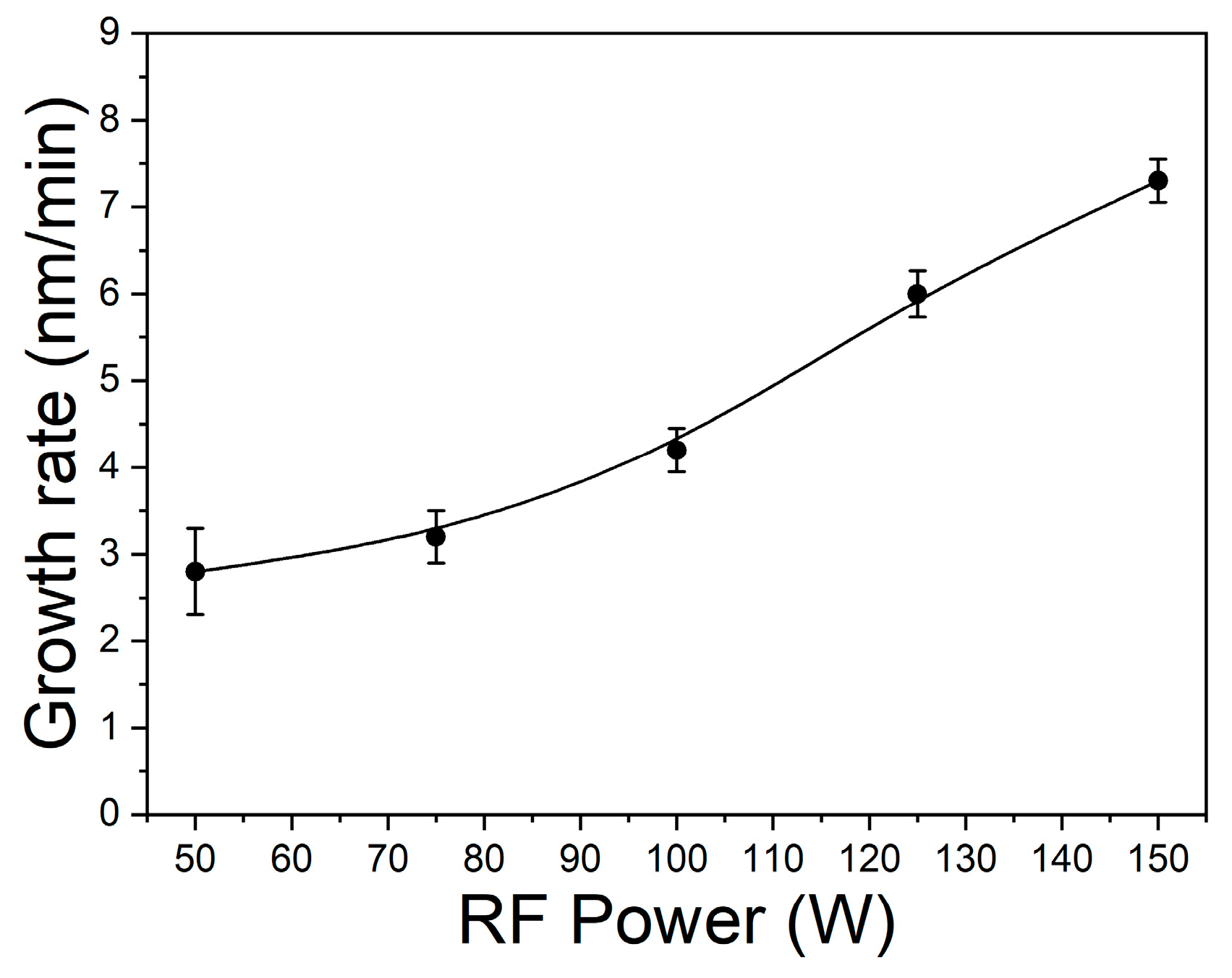
The influence of RF power supplied to the B4C target on the composition and properties of the as-grown BCx films was studied in this work. The thickness of the prepared films was 200–300 nm. Figure 2 shows the dependence of film growth rate on the B4C target sputtering power for series A. The growth rate of the films increased with increasing RF power (up to 7.3 nm/min at 150 W), which is typical for ion-plasma processes [20].
3.1. Film Structure, Composition, and Bonding Types
According to the SEM study, the surface of all the films was smooth, and no features were revealed, indicating that a change in power does not affect the morphology of the deposited layers and the films could be amorphous. This result was confirmed by the XRD data. The XRD patterns of all the films did not contain any reflexes (Figure S1). It is known that BCx films obtained by magnetron sputtering have an amorphous structure when synthesized up to 900 °C. [48].
The EDX analysis showed that the samples contained in their composition atoms of boron, carbon, and some oxygen. A small amount of nitrogen embedded in the films was observed; its amount does not exceed 3%. The oxygen probably came from the residual water or oxygen adsorbed in the reaction chamber during the deposition process and may be due to the film surface contamination after deposition during storage of the samples. The content of the elements in the as-grown films of series A is shown in Figure 3. It can be observed that an increase in the RF power applied to the B4C target resulted in a slight increase in the content of boron and carbon, and a decrease in the oxygen content. The same tendency of oxygen decreasing with increasing applied RF power was obtained by the authors of [20]. A decrease in the oxygen content in the film with an increase in the plasma power is explained by an increase in the particle energy, at which the probability of the collision of particles decreases [49]. As seen from Figure 3, the atomic ratio of boron to carbon is lower than the stoichiometry of B4C, which is consistent with the results of other investigations [49,50,51]. It should be noted that most authors of works where boron carbide films were deposited using a B4C target do not provide the data on the total elemental composition of these films or the ratio of B/C atoms, and do not mention the content of oxygen and nitrogen [48,52,53]. Table 3 presents atomic concentrations of dual-target sputtered samples of series B prepared using B4C and C targets in comparison with the A150 sample. The use of dual sputtering led to a significant change in chemical composition. The expected sharp increase in the carbon content in the film was observed. The atomic ratio of B/C equal to about 2/1 was obtained at a single sputtering of the B4C target, whereas at dual sputtering of B4C and C targets, the ratio of B/C equal to about 1/2 was obtained.
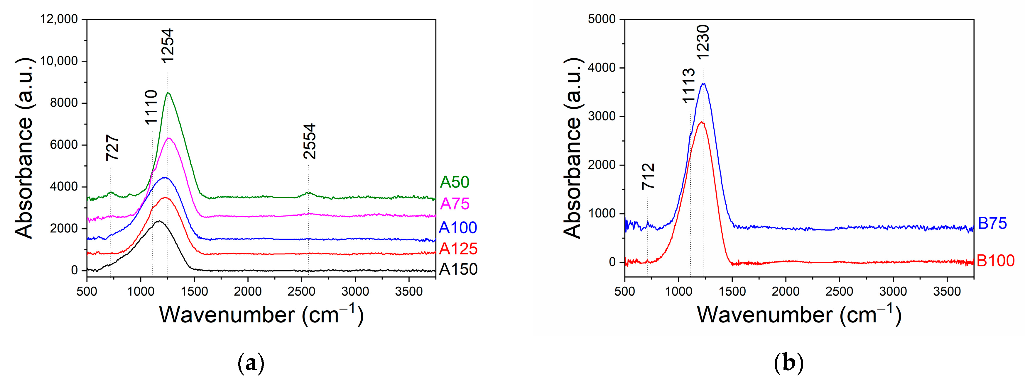
FTIR-spectroscopy was used for the study of chemical bonding. According to literature data, the spectrum of polycrystalline B4C has two bands near 1090 cm−1 (Eu) and 1580 (A2u) that are associated with vibrations of the icosahedron and chains connecting the icosahedra to each other, respectively [54,55,56]. The IR spectrum of amorphous boron carbide has a band at 1100 cm−1, which shifts to more than 1200 cm−1 for carbon-enriched a-B1-xCx films [32]. The absorbance bands associated with boron oxide appear in the IR-spectra at 1420 cm−1 (B–O stretching), 1280 cm−1 (B–O deformation), and 724 cm−1 (B–O deformation) [57]. The evolution of the FTIR spectra of the samples of series A is presented in Figure 4. The broad absorption bands with maximums in the region of 1152–1254 cm−1 are exhibited. With an increase of RF power applied to the B4C target from 50 to 150 W (Figure 4a), the maximum of the main band shifted to the region of low-frequency vibrations. This is apparently due to an increase in the proportion of B–C bonds. According to the EDX data, the concentration of boron and carbon rose with increasing power. The main peak of the A50 film spectrum can contain the contribution of B–O deformation vibrations that appeared at 1280 cm−1, which correlated with the EDX data on oxygen presence. Also, the FTIR spectrum of this sample contains a weak peak at 2554 cm−1 which corresponds to stretching vibrations of the B–H bond. The carbon-rich B75 and B100 samples prepared at dual magnetron sputtering (Figure 4b) also contain the broad absorption bands centered at 1230 and 1215 cm−1, respectively.
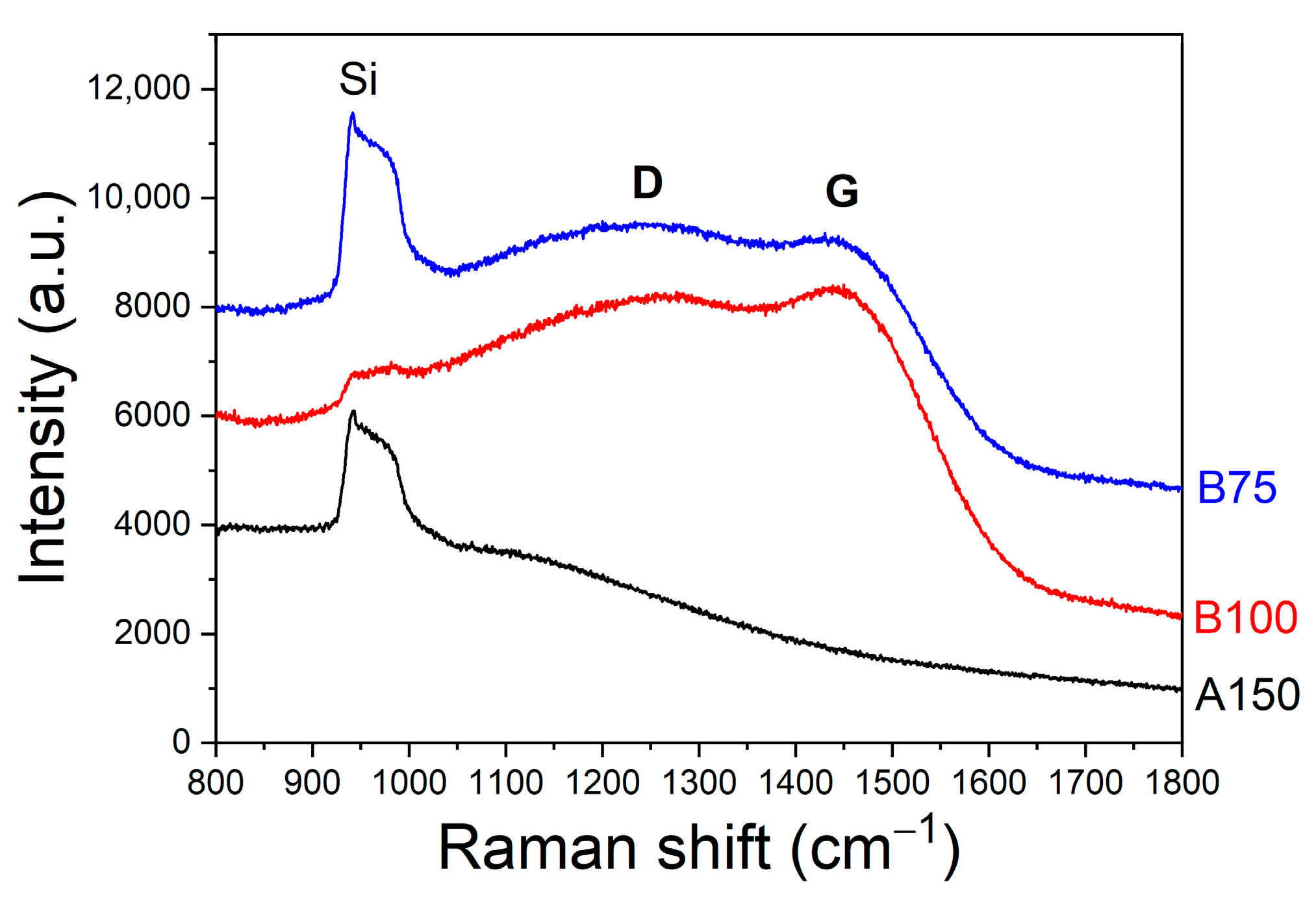
The Raman analysis of all the deposited BCx thin films revealed no vibrational modes corresponding to boron carbide (Figure 5) [58,59]. The Raman spectra of the carbon-rich samples of series B contain two broad bands corresponding to D and G modes of the amorphous carbon phase [60,61]. Whereas the G band is associated with the E2g in-plane graphite Raman active mode, the D band is a breathing mode of the A1g symmetry of the sixfold ring. Moreover, these bands were shifted to the left; this shift can be observed for BCx films due to amorphization and a decrease in the size of carbon particles [12]. It should be noted that the low intensity and broadening of the D and G bands indicate a strong carbon disordering. Thus, the carbon-rich samples contain carbon clusters. As noted above, according to the B–C phase diagram, solubility of carbon in B4C does not exceed 20 at.%. Therefore, carbon at higher concentrations should be expected to separate into an additional phase. On the other hand, there is information that this limitation is removed in amorphous boron carbide [62]. Despite the excess of carbon content compared with the permissible but not much higher (C = 25–30 at.%), the Raman spectra of the samples of series A did not show any peaks except for the Si substrate.
The analysis of B1s, C1s, N1s, and O1s the XPS spectra decomposed into components provides more detailed information on the chemical structure of the samples. The XPS spectra of the deposited films were recorded in order to reveal the effect of the power supplied to the RF magnetron using dual-target sputtering. It should be noted that XPS allows for the analysis of only ~9 nm of the film surface. XPS measurements were carried out without preliminary surface chemical etching or Ar+ sputtering to avoid preferential sputtering of B or C atoms. Therefore, the composition of the surface and the bulk material can be significantly different. Figure 6 shows the core level spectra of the B1s, C1s, and O1s of the A50, A150, and B75 films. The large width of XPS lines indicates a nonuniform chemical environment of boron and carbon atoms in the films. These peaks have complex structures and are superpositions of several components with different contributions.
The spectra of A150 and B75 show identical components with various intensities. Peaks in the region of 188.6–189.6 eV can be attributed to boron bonded to carbon in BCx. According to the literature data, the binding energies of B4C and BC3,4 compounds are 188.4 eV and 189.5 eV, respectively [63]. For the A150 sample, the maximum amount of boron in the film was found, and an increase in the component with Eb = 188.6 eV was observed. As the sputtering power is reduced, such a component is practically not observable in the XPS spectra. The peaks with binding energies in the region of 191–192.6 eV can be attributed to boron atoms bonded to carbon and oxygen atoms simultaneously; a component with a lower binding energy corresponds to the BC2O environment [64,65,66], with higher Eb to BCO2 [42,65,66]. Thus, low-power films have a strongly oxidized surface. According to the EDX analysis data, these films contain 19 at.% oxygen. It should be noted that the survey spectrum also contained the N1s peak, which indicates the presence of nitrogen in the films. Thus, a component near 191 eV can also be associated with B–N bonds [67]. The component with a binding energy of 193.4 eV apparently refers to boron atoms bound with oxygen [67,68]. In the C1s spectra, the two most intense peaks with binding energies of 283.0–283.7 eV and 285.3 eV are observed. The peak in the region of 283–284 eV corresponds to carbon atoms bound to boron [63,69]. The peak centered at 285 eV is, apparently, associated mainly with the C–C bonds. The high energy components (287.0 eV, 289.2 eV) could be attributed to the presence of carbon in the composition of different oxygen-containing groups. For the B75 and A150 samples, obtained with and without the carbon target, respectively, the peak intensity ratios corresponding to the C–C and C–B bonds are close. The decrease in the target power to 50 W led to the more significant contribution of the C–C bonds in comparison with the C–B bonds in the C1s spectrum. The O1s spectra can be fit to components at 532.5 eV, 533.2 eV, and 533.6 eV, assigned to O–C [70], O–B [71], and -OH [72] bonds, correspondingly. These values of Eb are typical for analogous systems [68]. However, it should be noted that the analysis of O1s spectra is associated with several difficulties, the main of which is the proximity of the energies of various oxygen-containing bonds in the studied system. As a result, the deconvolution into spectral components can only be qualitative.
3.2. Functional Properties of Films
The refractive index of the samples of series A varied in the range of 1.75–2.91 (Figure 7) and increased with increasing B4C target power. The rise of the refractive index is, apparently, associated with an increase in the proportion of B–C bonds in the films. The refractive index values of B75 and B100 films were equal to 2.43 and 2.62, respectively. Transmittance of the BCx film/fused silica structures was in the range of 60–75% in the visible region of spectra and increased with the decreasing B4C target power (Figure 8). Carbon-rich The BCx films exhibited a redshift of the absorption edge with increasing carbon incorporation. This obviously deals with the absorbance properties of carbon, the concentration of which is higher at higher power as was shown in Table 3. The optical band gap Eg was estimated as a result of absorption edge processing according to the Tauc law [73]. The Eg value decreased from 2.8 to 2.1 eV with increasing B4C target power. The lowest band gaps equal to 1.4 and 1.1 eV were reached for the B75 and B100 samples, respectively. These results are in good agreement with the literature data [20,74].
The hardness (Hf) and Young’s modulus (Ef) of the films of series A were 7–25 GPa and 100–230 GPa, respectively, and increased with increasing RF target power (Figure 9a). As seen from Figure 6 (B1s XPS spectra), higher values of sputtering power led to an increase in the proportion of B–C bonds. This suggests that in the films, the B–C bonding plays an important role in determining the mechanical property of the network due to the B–C bond being a more rigid covalent bond [75]. Unfavourable chemical bonds involving oxygen may be the possible origins of decreasing hardness and elastic modulus values with decreasing sputtering power values for the BCx films. It should be noted that, according to [37,76], the hardness and Young’s modulus of crystalline B4C are 25–40 GPa and 441–472 GPa, respectively, while the hardness and elastic modulus of amorphous BCx films with carbon concentrations of 21–44 at.% prepared by pulse DC MS at room temperature and a power of 130 W were comparable to our results and were equal to 18–29 GPa and 198–247 GPa, respectively [1]. Also, similar hardness values (20–28 GPa) were obtained for BCx films with carbon concentration changing from 19 at.% to 76 at.% deposited at 200 °C by pulse DC MS using B (880 W) and C (220–1750 W) targets [23], while boron carbide film prepared at 250 °C by DC MS (500 W) had a higher value equal to 34 GPa [21].
Unlike the films of series A, films of the series B had lower hardness values equal to 13–16 GPa (Table 4). Apparently, in the case of dual sputtering, the appearance of an additional phase of carbon, which was recorded by Raman spectroscopy, led to a decrease in the hardness value. According to the conclusions of the review [77], changes in hardness, as well as in other functional properties, depend on the carbon content in the homogeneity region of boron carbide. It should be emphasized that the maximum hardness was observed at a stoichiometric composition, and, for nonstoichiometric B4C materials (B/C > 4), decreased with increasing boron content. On the other hand, the hardness of BCx (B/C < 4) also decreased in the presence of free carbon in the films [78].
As an effective way to determine the elastic limit for surface contact, the elasticity index (H/E) is widely used [79]. Also, the material resistance to plastic deformation is described by the plasticity index (H3/E2), which means that the higher the value of H3/E2, the more difficult will be the shear steps [80]. In addition, the fracture toughness of a thin solid film can also be described in terms of measured hardness and Young’s modulus as H3/E2 ratio [79]. Therefore, these two parameters are undoubtedly important for preventing wear and the coating with optimized hardness, H/E, and H3/E2 are expected to exhibit exceptional wear resistance. Figure 9b illustrates that the elasticity index H/E and plasticity index H3/E2 of the BCx films reached the maximum value at 125 W of B4C target power.
Although the nanoindentation tests showed that the increase of C content in the coatings causes the decrease in their hardness, the H/E ratio of carbon-rich amorphous boron carbide coatings is rather high (about 0.1). Therefore, carbon-rich amorphous BCx coatings have potential as wear-resistant materials.
4. Conclusions
Amorphous BCx films with tailored carbon concentration were deposited by single and dual magnetron sputtering procedures on Si (100) and fused silica substrates at room temperature in ambient argon gas. A B4C target and C target were operated using an RF signal and a DC signal, respectively. The power on the B4C target was changed from 50 W to 150 W. The C target was operated at 75 W and 100 W. The dependences of the film properties on the target power were studied. The chemical composition of the BCx films was changed in the region of 0.5 ≤ x ≤ 2, wherein the composition of the films sputtered from the B4C target was weakly dependent on the target power. The deposition rate strongly depends on the power supplied to the B4C target. Depositions with the dual sputtering resulted in amorphous carbon phase incorporation into the boron carbide films. The transparency study of the BCx film showed that it depends on the above-mentioned experimental parameters. By tuning the B4C target power from 50 to 150 W, the BCx films exhibited carbon concentration change from 20 to 30 at.% and hardness and Young’s modulus of these films changed from 7 GPa to 25 GPa and from 100 GPa to 230 GPa, respectively. The maximum hardness, elasticity, and plasticity indexes of the BCx films were reached at the higher B4C target power. The results of optical and mechanical research have shown that the BCx films synthesized under “soft” conditions, namely at room temperature and with low sputtering powers (100–150 W), can be useful in optical applications in harsh environments.
Supplementary Materials
The following are available online at https://0-www-mdpi-com.brum.beds.ac.uk/article/10.3390/app11219896/s1, Figure S1: Typical (a) SEM image and (b) XRD pattern of BCx film.
Author Contributions
Conceptualization, M.K. (Marina Kosinova) and V.S.; methodology, V.S.; investigation, V.S. and M.K. (Maxim Khomyakov); writing—original draft preparation, V.S. and M.K. (Maxim Khomyakov); writing—review and editing, M.K. (Marina Kosinova) and V.S.; supervision, M.K. (Marina Kosinova); project administration, M.K. (Marina Kosinova); funding acquisition, M.K. (Marina Kosinova). All authors have read and agreed to the published version of the manuscript.
Funding
This research was funded by Ministry of Science and Higher Education of the Russian Federation, grant number FWUZ-2021-0006.
Institutional Review Board Statement
Not applicable.
Informed Consent Statement
Not applicable.
Acknowledgments
Not applicable.
Conflicts of Interest
The authors declare no conflict of interest.
References
- Wang, C.; Yang, Y.; Chung, Y.W.; Zhang, Y.; Ouyang, S.; Xiao, Z.; Song, K.; Li, P. Microstructure, Hardness and Toughness of Boron Carbide Thin Films Deposited by Pulse Dc Magnetron Sputtering. Ceram. Int. 2016, 42, 6342–6346. [Google Scholar] [CrossRef]
- Li, Y.Q.; Qiu, T. Oxidation Behaviour of Boron Carbide Powder. Mater. Sci. Eng. A 2007, 444, 184–191. [Google Scholar] [CrossRef]
- Moreno Fernández, H.; Rogler, D.; Sauthier, G.; Thomasset, M.; Dietsch, R.; Carlino, V.; Pellegrin, E. Characterization of Carbon-Contaminated B4C-Coated Optics after Chemically Selective Cleaning with Low-Pressure RF Plasma. Sci. Rep. 2018, 8, 1293. [Google Scholar] [CrossRef] [PubMed] [Green Version]
- Annen, A.; Von Keudell, A.; Jacob, W. Erosion of Amorphous Hydrogenated Boron-Carbon Thin Films. J. Nucl. Mater. 1996, 231, 151–154. [Google Scholar] [CrossRef]
- Lin, S.H.; Feldman, B.J.; Li, D. Microhardness Study of Amorphous Hydrogenated Boron Carbide Deposited on a Cathode Substrate by Plasma Deposition. Appl. Phys. Lett. 1996, 69, 2373–2375. [Google Scholar] [CrossRef]
- Suri, A.K.; Subramanian, C.; Sonber, J.K.; Murthy, T.S.R.C. Synthesis and Consolidation of Boron Carbide: A Review. Int. Mater. Rev. 2010, 55, 4–40. [Google Scholar] [CrossRef]
- Byun, D.; Spady, B.R.; Ianno, N.J.; Dowben, P.A. Comparison of Different Chemical Vapor Deposition Methodologies for the Fabrication of Heterojunction Boron-Carbide Diodes. Nanostructured Mater. 1995, 5, 465–471. [Google Scholar] [CrossRef]
- Hwang, S.D.; Byun, D.; Ianno, N.J.; Dowben, P.A.; Kim, H.R. Fabrication of Boron-Carbide/Boron Heterojunction Devices. Appl. Phys. Lett. 1996, 68, 1495–1497. [Google Scholar] [CrossRef] [Green Version]
- Sennikov, P.G.; Kornev, R.A.; Shishkin, A.I. Preparation of Boron Carbide from BF3 and BCl3 in Hydrogen Plasma of Arc RF Discharge. Plasma Chem. Plasma Process. 2017, 37, 997–1008. [Google Scholar] [CrossRef]
- Li, S.; Zeng, B.; Feng, Z.; Liu, Y.; Yang, W.; Cheng, L.; Zhang, L. Effects of Heat Treatment on the Microstructure of Amorphous Boron Carbide Coating Deposited on Graphite Substrates by Chemical Vapor Deposition. Thin Solid Films 2010, 519, 251–258. [Google Scholar] [CrossRef]
- Cholet, V.; Herbin, R.; Vandenbulcke, L. Chemical Vapour Deposition of Boron Carbide from BBr3-CH4-H2 Mixtures in a Microwave Plasma. Thin Solid Films 1990, 188, 143–155. [Google Scholar] [CrossRef]
- Imam, M.; Höglund, C.; Jensen, J.; Schmidt, S.; Ivanov, I.G.; Hall-Wilton, R.; Birch, J.; Pedersen, H. Trimethylboron as Single-Source Precursor for Boron-Carbon Thin Film Synthesis by Plasma Chemical Vapor Deposition. J. Phys. Chem. C 2016, 120, 21990–21997. [Google Scholar] [CrossRef] [Green Version]
- Pedersen, H.; Höglund, C.; Birch, J.; Jensen, J.; Henry, A. Low Temperature CVD of Thin, Amorphous Boron-Carbon Films for Neutron Detectors. Chem. Vap. Depos. 2012, 18, 221–224. [Google Scholar] [CrossRef] [Green Version]
- Imam, M.; Gaul, K.; Stegmüller, A.; Höglund, C.; Jensen, J.; Hultman, L.; Birch, J.; Tonner, R.; Pedersen, H. Gas Phase Chemical Vapor Deposition Chemistry of Triethylboron Probed by Boron-Carbon Thin Film Deposition and Quantum Chemical Calculations. J. Mater. Chem. C 2015, 3, 10898–10906. [Google Scholar] [CrossRef] [Green Version]
- Martin, A.A.; Depond, P.J.; Bagge-Hansen, M.; Lee, J.R.I.; Yoo, J.-H.; Elhadj, S.; Matthews, M.J.; van Buuren, T. Rapid Feedback of Chemical Vapor Deposition Growth Mechanisms by Operando X-Ray Diffraction. J. Vac. Sci. Technol. B 2018, 36, 020601. [Google Scholar] [CrossRef]
- Nordell, B.J.; Nguyen, T.D.; Caruso, A.N.; Purohit, S.S.; Oyler, N.A.; Lanford, W.A.; Gidley, D.W.; Gaskins, J.T.; Hopkins, P.E.; Henry, P.; et al. Carbon-Enriched Amorphous Hydrogenated Boron Carbide Films for Very-Low-k Interlayer Dielectrics. Adv. Electron. Mater. 2017, 3, 1700116. [Google Scholar] [CrossRef]
- Peterson, G.G.; Su, Q.; Wang, Y.; Ianno, N.J.; Dowben, P.A.; Nastasi, M. Improved A-B10C2+xHy/Si p-n Heterojunction Performance after Neutron Irradiation. J. Vac. Sci. Technol. B 2018, 36, 011207. [Google Scholar] [CrossRef] [Green Version]
- Vassallo, E.; Caniello, R.; Cremona, A.; Croci, G.; Dellasega, D.; Gorini, G.; Grosso, G.; Miorin, E.; Passoni, M.; Tardocchi, M. Deposition of Boron-Carbon Multilayer Coatings by RF Plasma Sputtering. Surf. Coat. Technol. 2013, 214, 59–62. [Google Scholar] [CrossRef]
- Bao, R.; Chrisey, D.B. Chemical States of Carbon in Amorphous Boron Carbide Thin Films Deposited by Radio Frequency Magnetron Sputtering. Thin Solid Films 2010, 519, 164–168. [Google Scholar] [CrossRef]
- Ahmad, A.A. Optical and Electrical Properties of Synthesized Reactive Rf Sputter Deposited Boron-Rich and Boron-Doped Diamond-like Carbon Thin Films. J. Mater. Sci. Mater. Electron. 2017, 28, 1695–1705. [Google Scholar] [CrossRef]
- Tavsanoglu, T.; Jeandin, M.; Addemir, O.; Tavsanoglu, T.; Jeandin, M.; Addemir, O. Synthesis and Characterisation of Thin Films in the B–C–N Triangle. Surf. Eng. 2016, 32, 755–760. [Google Scholar] [CrossRef]
- Kulikovsky, V.; Vorlicek, V.; Bohac, P.; Ctvrtlik, R.; Stranyanek, M.; Dejneka, A.; Jastrabik, L. Mechanical Properties and Structure of Amorphous and Crystalline B4C Films. Diam. Relat. Mater. 2009, 18, 27–33. [Google Scholar] [CrossRef]
- Qian, J.C.; Zhou, Z.F.; Yan, C.; Li, D.J.; Li, K.Y.; Descartes, S.; Chromik, R.; Zhang, W.J.; Bello, I.; Martinu, L.; et al. Tailoring the Mechanical and Tribological Properties of Sputtered Boron Carbide Films via the B1-XCx Composition. Surf. Coat. Technol. 2015, 267, 2–7. [Google Scholar] [CrossRef]
- Castillo, H.A.; Restrepo-Parra, E.; Vélez, J.M.; de la Cruz, W. Substrate Temperature Influence on Boron Carbide Coatings Grown by the PLD Technique. Surf. Coat. Technol. 2011, 205, 3607–3612. [Google Scholar] [CrossRef]
- Zhang, S.; Lu, W.; Wang, C.; Shen, Q.; Zhang, L. Stoichiometric Controlling of Pulsed Laser Deposited Boron-Carbon Thin Films. Phys. B Condens. Matter 2012, 407, 2382–2384. [Google Scholar] [CrossRef]
- Gago, R.; Jiménez, I.; Agulló-Rueda, F.; Albella, J.M.; Czigány, Z.; Hultman, L. Transition from Amorphous Boron Carbide to Hexagonal Boron Carbon Nitride Thin Films Induced by Nitrogen Ion Assistance. J. Appl. Phys. 2002, 92, 5177–5182. [Google Scholar] [CrossRef]
- Sasaki, S.; Takeda, M.; Yokoyama, K.; Miura, T.; Suzuki, T.; Suematsu, H.; Jiang, W.; Yatsui, K. Thermoelectric Properties of Boron-Carbide Thin Film and Thin Film Based Thermoelectric Device Fabricated by Intense-Pulsed Ion Beam Evaporation. Sci. Technol. Adv. Mater. 2005, 6, 181–184. [Google Scholar] [CrossRef] [Green Version]
- Pristáš, G.; Werheit, H.; Gabáni, S.; Shalamberidze, S.; Flachbart, K. Low Temperature Specific Heat Anomaly with Boson Peak in Isotope-Enriched Boron Carbides B4·3C–B10C. Solid State Sci. 2020, 101, 106140. [Google Scholar] [CrossRef]
- Beauvy, M. Stoichiometric Limits of Carbon-Rich Boron Carbide Phases. J. Less-Common Met. 1983, 90, 169–175. [Google Scholar] [CrossRef]
- Konovalikhin, S.V.; Ponomarev, V.I. Carbon in Boron Carbide: The Crystal Structure of B11.4C 3.6. Russ. J. Inorg. Chem. 2009, 54, 197–203. [Google Scholar] [CrossRef]
- Werheit, H.; Shalamberidze, S. Advanced Microstructure of Boron Carbide. J. Phys. Condens. Matter 2012, 24, 385406. [Google Scholar] [CrossRef] [PubMed]
- Shirai, K.; Emura, S.; Gonda, S.I.; Kumashiro, Y. Infrared Study of Amorphous B1-XCx Films. J. Appl. Phys. 1995, 78, 3392–3400. [Google Scholar] [CrossRef]
- An, Q.; Goddard, W.A. Nanotwins Soften Boron-Rich Boron Carbide (B13C2). Appl. Phys. Lett. 2017, 110, 111902. [Google Scholar] [CrossRef] [Green Version]
- Xie, K.Y.; Domnich, V.; Farbaniec, L.; Chen, B.; Kuwelkar, K.; Ma, L.; McCauley, J.W.; Haber, R.A.; Ramesh, K.T.; Chen, M.; et al. Microstructural Characterization of Boron-Rich Boron Carbide. Acta Mater. 2017, 136, 202–214. [Google Scholar] [CrossRef]
- Cheng, C.; Reddy, K.M.; Hirata, A.; Fujita, T.; Chen, M. Structure and Mechanical Properties of Boron-Rich Boron Carbides. J. Eur. Ceram. Soc. 2017, 37, 4514–4523. [Google Scholar] [CrossRef]
- Imam, M.; Souqui, L.; Herritsch, J.; Stegmüller, A.; Höglund, C.; Schmidt, S.; Hall-Wilton, R.; Högberg, H.; Birch, J.; Tonner, R.; et al. Gas Phase Chemistry of Trimethylboron in Thermal Chemical Vapor Deposition. J. Phys. Chem. C 2017, 121, 26465–26471. [Google Scholar] [CrossRef]
- Zhen-Jie, Q.; Le, G.A.O.; Qian, F.; Jian-Bao, H.U.; Shao-Ming, D.; Liang-Lai, M.A. Boron Content on Microstructure and Mechanical Properties of Amorphous Boron Carbide by Chemical Vapor Deposition Films Preparation. J. Inorg. Mater. 2017, 32, 1228–1232. [Google Scholar] [CrossRef]
- Ektarawong, A.; Simak, S.I.; Alling, B. Carbon-Rich Icosahedral Boron Carbides beyond B4C and Their Thermodynamic Stabilities at High Temperature and Pressure from First Principles. Phys. Rev. B 2016, 94, 054104. [Google Scholar] [CrossRef] [Green Version]
- Kevill, D.N.; Rissmann, T.J.; Brewe, D.; Wood, C. Growth of Crystals of Several Boron-Carbon Compositions by Chemical Vapor Deposition. J. Cryst. Growth 1986, 74, 210–216. [Google Scholar] [CrossRef]
- Deng, J.L.; Cheng, L.F.; Gao, L.N.; Su, K.H. The Relationship between the Initial Gas Ratios and the Condensed Phase Composition in the CVD of BxC with BCl3-CH4-H2 Precursors. Adv. Mater. Res. 2011, 239–242, 1761–1765. [Google Scholar] [CrossRef]
- Zeng, B.; Feng, Z.D.; Li, S.W.; Liu, Y.S. Microstructural Study of Oxidation of Carbon-Rich Amorphous Boron Carbide Coating. Front. Mater. Sci. China 2008, 2, 375–380. [Google Scholar] [CrossRef]
- He, D.; Shang, L.; Lu, Z.; Zhang, G.; Wang, L.; Xue, Q. Tailoring the Mechanical and Tribological Properties of B4C/a-C Coatings by Controlling the Boron Carbide Content. Surf. Coat. Technol. 2017, 329, 11–18. [Google Scholar] [CrossRef]
- Larruquert, J.I.; Pérez-Marín, A.P.; García-Cortés, S.; Rodríguez-de Marcos, L.; Aznárez, J.A.; Méndez, J.A. Self-Consistent Optical Constants of Sputter-Deposited B4C Thin Films. J. Opt. Soc. Am. A 2012, 29, 117–123. [Google Scholar] [CrossRef] [Green Version]
- Sulyaeva, V.S.; Maksimovskii, E.A.; Kosinova, M.L.; Rumyantsev, Y.M. Analysis Features of Elemental Composition of Boron Carbonitride Films by EDS. Prot. Met. Phys. Chem. Surf. 2014, 50, 273–277. [Google Scholar] [CrossRef]
- Korsunsky, A.M.; McGurk, M.R.; Bull, S.J.; Page, T.F. On the Hardness of Coated Systems. Surf. Coat. Technol. 1998, 99, 171–183. [Google Scholar] [CrossRef]
- Doerner, M.F.; Nix, W.D. A Method for Interpreting the Data from Depth-Sensing Indentation Instruments. J. Mater. Res. 1986, 1, 601–609. [Google Scholar] [CrossRef]
- Useinov, A.; Kravchuk, K.; Maslenikov, I. Measurement of Hardness and Fracture Toughness of Solid Coatings. Nanoindustry 2013, 7, 48–56. Available online: https://www.nanoindustry.su/files/article_pdf/3/article_3944_301.pdf (accessed on 18 October 2021).
- Kim, T.S.; Yeo, J.H.; Nam, K.B.; Kim, M.J.; Yoo, J.B. Boron Carbide Coating to Improve the Chemical Stability of Nm-Thick Graphite Films. Thin Solid Films 2020, 704, 138002. [Google Scholar] [CrossRef]
- Jensen, J.; Hultman, L.; Birch, J.; Schmidt, S.; Ho, C.; Hall-wilton, R. Low-Temperature Growth of Boron Carbide Coatings by Direct Current Magnetron Sputtering and High-Power Impulse Magnetron Sputtering. J. Mater. Sci. 2016, 51, 10418–10428. [Google Scholar] [CrossRef] [Green Version]
- Cao, X.; Shang, L.; Liang, Y.; Zhang, G.; Lu, Z.; Xue, Q. The Tribological Performances of the Boron Carbide Films Tested under Wet Air and Wet N2 Conditions. Tribol. Lett. 2019, 67, 1–11. [Google Scholar] [CrossRef]
- Salas, E.; Jiménez Riobóo, R.J.; Sánchez-Marcos, J.; Jiménez-Villacorta, F.; Muñoz-Martín, A.; Prieto, J.E.; Joco, V.; Prieto, C. Elastic Properties of B-C-N Films Grown by N2-Reactive Sputtering from Boron Carbide Targets. J. Appl. Phys. 2013, 114, 213508. [Google Scholar] [CrossRef] [Green Version]
- Störmer, M.; Siewert, F.; Horstmann, C.; Buchheim, J.; Gwalt, G. Coatings for FEL Optics: Preparation and Characterization of B4C and Pt. J. Synchrotron Radiat. 2018, 25, 116–122. [Google Scholar] [CrossRef] [Green Version]
- Baik, Y.J.; Bae, K.E.; Park, J.-K.; Lee, W.-S. Oxidation Behavior of Amorphous Boron Carbide Film Deposited Using the Unbalanced Magnetron Sputtering Method. Korean J. Met. Mater. 2016, 54, 8–14. [Google Scholar] [CrossRef]
- Werheit, H. Optical Phonons of Boron Carbide Depending on the Composition. J. Less-Common Met. 1986, 117, 17–20. [Google Scholar] [CrossRef]
- Stein, H.; Aselage, T.; Emin, D. Infrared Absorption in Boron Carbides: Dependence on Isotopes and Carbon Concentration. AIP Conf. Proc. 1991, 231, 322–325. [Google Scholar] [CrossRef]
- Werheit, H.; Manghnani, M.H.; Hushur, A. Phonon Peculiarities at the High-Pressure Phase Transition of B4.3C Boron Carbide. Solid State Sci. 2019, 97, 105978. [Google Scholar] [CrossRef]
- Weltner, W.; Warn, J.R.W. Matrix Isolation of High-Temperature Vapors: Boric Oxide. J. Chem. Phys. 1962, 37, 292–303. [Google Scholar] [CrossRef]
- Tallant, D.R.; Aselage, T.L.; Campbell, A.N.; Emin, D. Boron Carbide Structure by Raman Spectroscopy. Phys. Rev. B 1989, 40, 5649–5656. [Google Scholar] [CrossRef]
- Werheit, H.; Filipov, V.; Kuhlmann, U.; Schwarz, U.; Armbrüster, M.; Leithe-Jasper, A.; Tanaka, T.; Higashi, I.; Lundström, T.; Gurin, V.N.; et al. Raman Effect in Icosahedral Boron-Rich Solids. Sci. Technol. Adv. Mater. 2010, 11, 023001. [Google Scholar] [CrossRef] [PubMed] [Green Version]
- Zinin, P.V.; Ming, L.C.; Kudryashov, I.; Konishi, N.; Sharma, S.K. Raman Spectroscopy of the BC3 Phase Obtained under High Pressure and High Temperature. J. Raman Spectrosc. 2007, 38, 1362–1367. [Google Scholar] [CrossRef]
- Ferrari, A.C.; Robertson, J. Interpretation of Raman Spectra of Disordered and Amorphous Carbon. Phys. Rev. B 2000, 61, 14095–14107. [Google Scholar] [CrossRef] [Green Version]
- Anan’ev, A.S.; Kon’kov, O.I.; Lebedev, V.M.; Novokhatski, A.N.; Terukov, E.I.; Trapeznikova, I.N. Fabrication and Properties of Amorphous Hydrogenated Boron Carbide Films. Semiconductors 2002, 36, 941–943. [Google Scholar] [CrossRef]
- Künzli, H.; Gantenbein, P.; Steiner, R.; Oelhafen, P. Deposition and Characterization of Thin Boron-Carbide Coatings. Fresenius J. Anal. Chem. 1993, 346, 41–44. [Google Scholar] [CrossRef]
- Susi, T.; Pichler, T.; Ayala, P. X-Ray Photoelectron Spectroscopy of Graphitic Carbon Nanomaterials Doped with Heteroatoms. Beilstein J. Nanotechnol. 2015, 6, 177–192. [Google Scholar] [CrossRef] [Green Version]
- Shen, W.; Li, H.; Wang, C.; Li, Z.; Xu, Q.; Liu, H.; Wang, Y. Improved Electrochemical Performance of the Na3V2(PO4)3 Cathode by B-Doping of the Carbon Coating Layer for Sodium-Ion Batteries. J. Mater. Chem. A 2015, 3, 15190–15201. [Google Scholar] [CrossRef]
- Wang, H.; Li, Y.; Wang, Y.; Hu, S.; Hou, H. Highly Microporous Graphite-like BCxO3−x/C Nanospheres for Anode Materials of Lithium-Ion Batteries. J. Mater. Chem. A 2017, 5, 2835–2843. [Google Scholar] [CrossRef]
- Paul, R.; Voevodin, A.A.; Zemlyanov, D.; Roy, A.K.; Fisher, T.S. Microwave-Assisted Surface Synthesis of a Boron-Carbon-Nitrogen Foam and Its Desorption Enthalpy. Adv. Funct. Mater. 2012, 22, 3682–3690. [Google Scholar] [CrossRef]
- Tsai, P.C. The Deposition and Characterization of BCN Films by Cathodic Arc Plasma Evaporation. Surf. Coat. Technol. 2007, 201, 5108–5113. [Google Scholar] [CrossRef]
- Yang, Q.; Wang, C.B.; Zhang, S.; Zhang, D.M.; Shen, Q.; Zhang, L.M. Effect of Nitrogen Pressure on Structure and Optical Properties of Pulsed Laser Deposited BCN Thin Films. Surf. Coat. Technol. 2010, 204, 1863–1867. [Google Scholar] [CrossRef]
- Chen, C.M.; Huang, J.Q.; Zhang, Q.; Gong, W.Z.; Yang, Q.H.; Wang, M.Z.; Yang, Y.G. Annealing a Graphene Oxide Film to Produce a Free Standing High Conductive Graphene Film. Carbon 2012, 50, 659–667. [Google Scholar] [CrossRef]
- Moon, O.M.; Kang, B.C.; Lee, S.B.; Boo, J.H. Temperature Effect on Structural Properties of Boron Oxide Thin Films Deposited by MOCVD Method. Thin Solid Films 2004, 464–465, 164–169. [Google Scholar] [CrossRef]
- Beamson, G.; Briggs, D. High Resolution XPS of Organic Polymers: The Scienta ESCA300 Database; Wiley: New York, NY, USA, 1992. [Google Scholar]
- Sulyaeva, V.S.; Rumyantsev, Y.M.; Kesler, V.G.; Kosinova, M.L. Synthesis and Optical Properties of BCxNy Films Deposited from N-Triethylborazine and Hydrogen Mixture. Thin Solid Films 2015, 581, 59–64. [Google Scholar] [CrossRef]
- Nehate, S.D.; Saikumar, A.K.; Sundaram, K.B. Influence of Substrate Temperature on Electrical and Optical Properties of Hydrogenated Boron Carbide Thin Films Deposited by Rf Sputtering. Coatings 2021, 11, 196. [Google Scholar] [CrossRef]
- Zhang, S.; Wu, J.; Yang, Q.; Tu, R.; Wang, C.; Shen, Q.; Zhang, L. Stoichiometric Controlling of Boroncarbonitride Thin Films with Using BN-C Dual-Targets. AIP Adv. 2015, 5, 047125. [Google Scholar] [CrossRef] [Green Version]
- Domnich, V.; Reynaud, S.; Haber, R.A.; Chhowalla, M. Boron Carbide: Structure, Properties, and Stability under Stress. J. Am. Ceram. Soc. 2011, 94, 3605–3628. [Google Scholar] [CrossRef]
- Andrievski, R.A. Micro- and Nanosized Boron Carbide: Synthesis, Structure and Properties. Russ. Chem. Rev. 2012, 81, 549–559. [Google Scholar] [CrossRef]
- Niihara, K.; Nakahira, A.; Hirai, T. The Effect of Stoichiometry on Mechanical Properties of Boron Carbide. Commun. Am. Ceram. Soc. 1984, 6, C-13–C-14. [Google Scholar] [CrossRef]
- Leyland, A.; Matthews, A. On the Significance of the H/E Ratio in Wear Control: A Nanocomposite Coating Approach to Optimised Tribological Behaviour. Wear 2000, 246, 1–11. [Google Scholar] [CrossRef]
- Tsui, T.Y.; Pharr, G.M.; Oliver, W.C.; Bhatia, C.S.; White, R.L.; Anders, S.; Anders, A.; Brown, I.G. Nanoindentation and Nanoscratching of Hard Carbon Coatings for Magnetic Disks. In Proceedings of the Spring Meeting of the Materials Research Society (MRS), San Francisco, CA, USA, 17–21 April 1995; Volume 383, pp. 447–452. [Google Scholar]
Figure 1.
Dependence of (a) hardness and (b) Young’s modulus on the indentation depth for the BCx films.
Figure 1.
Dependence of (a) hardness and (b) Young’s modulus on the indentation depth for the BCx films.

Figure 2.
Deposition rate of the boron carbide films as a function of B4C target power.

Figure 3.
B, C, and O elemental composition of boron carbide films versus RF power at B4C target.

Figure 4.
FTIR spectra of samples of (a) series A and (b) series B.

Figure 5.
Raman spectra of boron carbide films.

Figure 6.
(a) B1s, (b) C1s, and (c) O1s core-level spectra of A50, A150, and B75 films.

Figure 7.
Refractive index of samples versus B4C target power (series A).

Figure 8.
Effect of (a) B4C target power and (b) C target power on transmittance of samples.

Figure 9.
Dependences of (a) hardness (black line), Young’s modulus (red line), and (b) the elasticity index H/E and plasticity index H3/E2 of samples on B4C target power (series A).
Figure 9.
Dependences of (a) hardness (black line), Young’s modulus (red line), and (b) the elasticity index H/E and plasticity index H3/E2 of samples on B4C target power (series A).


Table 1.
Selected literature data on the formation of boron- and carbon-rich boron carbide.
| Type of Boron Carbide | Deposition Method | Precursor/ Source | Temperature, °C | Chemical Composition | Ref. |
|---|---|---|---|---|---|
| B-rich | Calculation | – | – | B13C2 | [33] |
| B-rich | Laser CVD | B(OCH3)3 | – | B8C | [15] |
| B-rich | Hot pressing | B4C, B | 1900–2200 | B4.2C, B5.6C B7.6C | [34] |
| B-rich | Hot pressing | B4C, B | 1900–2200 | B4.6C, B6.5C, B7.8C, B10.2C | [35] |
| B-, C-rich | CVD | B(C2H5)3 | 700–1200 | B4.5C, B1.9C, BC11.5 | [14] |
| B-, C-rich | PLD | Sintered BC | – | B2.9–4.6C | [25] |
| B-, C-rich | CVD | BCl3, CCl4 | 1000–1275 | B0.95-0.65C0.04-0.35 | [39] |
| C-rich | Calculation | – | – | B0.67-0.80C0.33-0.20 | [38] |
| C-rich | CVD | B(CH3)3 | 700–1100 | B0.29-0.75C0.71-0.25 | [36] |
| C-rich | CVD | BCl3, C3H6 | 900 | BC19, BC9, BC5, B3C7, BC | [37] |
| C-rich | Calculation | BCl3, CH4 | 950–1000 | – | [40] |
| C-rich | MS | B, C | 200 | B0.81C0.19, B0.44C0.56, B0.24C0.76 | [23] |
Table 2.
Experimental conditions for magnetron sputtering of samples.
| Series | Sample | B4C Target Power, W | C Target Power, W |
|---|---|---|---|
| A | A50 | 50 | – |
| A75 | 75 | – | |
| A100 | 100 | – | |
| A125 | 125 | – | |
| A150 | 150 | – | |
| B | B75 | 150 | 75 |
| B100 | 150 | 100 |
Table 3.
Elemental composition of dual-target sputtered samples of series B.
| Sample | Atomic Concentration, at.% | ||
|---|---|---|---|
| B | C | O | |
| A150 | 66 | 30 | 4 |
| B75 | 51 | 44 | 5 |
| B100 | 27 | 68 | 5 |
Note: The absolute uncertainty of all values is ± 5%.
Table 4.
Mechanical properties of dual-target sputtered samples of series B.
| Sample | Hardness, GPa | E, GPa | H/E | H3/E2, GPa |
|---|---|---|---|---|
| B75 | 13.2 ± 2.2 | 152 ± 26 | 0.09 | 0.10 |
| B100 | 16.3 ± 1.5 | 214 ± 35 | 0.08 | 0.09 |
Publisher’s Note: MDPI stays neutral with regard to jurisdictional claims in published maps and institutional affiliations. |
© 2021 by the authors. Licensee MDPI, Basel, Switzerland. This article is an open access article distributed under the terms and conditions of the Creative Commons Attribution (CC BY) license (https://creativecommons.org/licenses/by/4.0/).
Share and Cite
MDPI and ACS Style
Sulyaeva, V.; Khomyakov, M.; Kosinova, M. Room-Temperature Formation of Hard BCx Films by Low Power Magnetron Sputtering. Appl. Sci. 2021, 11, 9896. https://0-doi-org.brum.beds.ac.uk/10.3390/app11219896
AMA Style
Sulyaeva V, Khomyakov M, Kosinova M. Room-Temperature Formation of Hard BCx Films by Low Power Magnetron Sputtering. Applied Sciences. 2021; 11(21):9896. https://0-doi-org.brum.beds.ac.uk/10.3390/app11219896
Chicago/Turabian StyleSulyaeva, Veronica, Maxim Khomyakov, and Marina Kosinova. 2021. "Room-Temperature Formation of Hard BCx Films by Low Power Magnetron Sputtering" Applied Sciences 11, no. 21: 9896. https://0-doi-org.brum.beds.ac.uk/10.3390/app11219896
Note that from the first issue of 2016, this journal uses article numbers instead of page numbers. See further details here.