Article

Orientation of Liquid Crystalline Molecules on PDMS Surfaces and within PDMS Microfluidic Systems

by
Szymon Baczyński
1,
Piotr Sobotka
1,
Kasper Marchlewicz
2,
Mateusz Słowikowski
3,
Marcin Juchniewicz
3,
Artur Dybko
2 and
Katarzyna A. Rutkowska
1,*
1
Faculty of Physics, Warsaw University of Technology, Koszykowa 75, 00-662 Warsaw, Poland
2
Faculty of Chemistry, Warsaw University of Technology, Noakowskiego 3, 00-664 Warsaw, Poland
3
Centre for Advanced Materials and Technologies (CEZAMAT), Warsaw University of Technology, Poleczki 19, 02-822 Warsaw, Poland
*
Author to whom correspondence should be addressed.
Submission received: 26 August 2021 / Revised: 19 November 2021 / Accepted: 24 November 2021 / Published: 7 December 2021
(This article belongs to the Special Issue Liquid Crystal Thin Films: Structures and Applications)

Abstract

:
The unique components of PDMS-based microfluidic systems are those combined with liquid crystalline materials. Their functionality, especially when it comes to optical applications, highly depends on the LC molecular arrangement. This work summarizes experimental investigations on the orientation of molecules within LC:PDMS structures according to the manufacturing technologies. The availability of high-quality molds to pattern PDMS is a significant barrier to the creation of advanced microfluidic systems. The possibility of using inexpensive molds in the rapid and reproducible fabrication process has been particularly examined as an alternative to photolithography. Different geometries, including an innovative approach for the electrical control of the molecular arrangement within PDMS microchannels, are presented. These studies are critical for novel optofluidic systems, introducing further research on LC:PDMS waveguiding structures.

1. Introduction

Microfluidic structures represent an essential part of modern photonic systems. Their varieties include, e.g., microfluidic chips, Lab-on-a-Chips (LOCs), Photonic Lab-on-a-Chips (PhLoCs), and micro-total-analysis-systems (µ-TASs), thus combining applications and technologies known from chemistry, biology, and photonics [1,2]. Owning to such solutions, space-consuming or expensive devices can be miniaturized, and the performed analyses or tests can be accelerated with significantly reduced costs [3,4,5]. This is particularly evident when inexpensive soft lithography is used for microfabrication, suiting many materials, including elastomeric ones. A considerable number of microfluidic structures are fabricated by a cast-molding technique using polydimethylsiloxane (PDMS). The latter may be successfully applied not only as a building material for the systems themselves but also as a mold for structures made of other materials [6,7]. However, the first scenario is prevalent for PDMS-embedded photonic devices, relying essentially on the availability of high-quality molds. The fabrication of microstructured master molds with the required geometrical features is objectively a critical step in the manufacturing process. Various techniques may be applied for this purpose, including micromilling [8,9,10], 3D printing [9,11,12], polystyrene thermoplastic sheet shrinkage [13], capillary film processing [14], and photolithography [15]. In addition, a combination of different methods [16] or additional improvements of existing ones—e.g., the smoothing of the stamp’s surfaces [17]—are also employed, resulting in high-quality micron-scale patterns to be accurately replicated in PDMS. In terms of optical applications, further benefits of such elastomer applications include its refractive index of about 1.41 @ 589 nm [18], isotropy, homogeneity, and high optical transparency in the spectral range covering UV, VIS, and NIR [19]. Examples of the microfluidic photonic structures obtained in PDMS are optofluidic sensing devices [20], optical MEMS [21], microlenses [22], dye lasers [23], and reconfigurable optical waveguides [24].
A particular part of the PDMS-based microfluidic systems is constituted by structures filled with liquid crystals (LCs). Exploiting such unique birefringent and anisotropic materials may lead to many intriguing phenomena with various potential applications of the so-formed LC:PDMS architectures. One of them is the hierarchical filtration or sampling of liquid crystalline biomaterials and chemicals in electrically programmable microfluidic structures [25]. LOC-integrable systems can also be applied to enclose liquid crystal lasers utilizing cholesteric liquid crystal (CLC) confined between PDMS substrates [26]. Another usage of CLC is biosensing chips for albumin detection [27]. A 1-kHz optofluidic modulator was used to achieve novel analytical and imaging methods based on peristaltic nematogen microflows [28], and the PDMS-based tunable optofluidic birefringent lens utilized nematic liquid crystals (NLCs) to obtain different focal distances for p- and s-polarized light [29]. At the same time, the polymer-dispersed liquid crystal (PDLC) structures are another area of research that offers excellent opportunities in microfluidics. For example, a carbon nanotube-liquid crystal-PDMS composite structure may be indicated to serve as a highly resistive pressure sensor [30]. Studies on optical waveguides represent an important research area involving LC:PDMS structures [31,32,33,34]. This is strongly encouraged by the low-cost and straightforward soft material technology allowing for arbitrary geometry. The maintenance of the polarization state for the light propagating along the microchannels embedded in PDMS and infiltrated with NLC indicates many potential arrangements for integrated optics and microfluidic circuits [35]. For instance, LC:PDMS waveguiding structures may be used to obtain reconfigurable optical interconnectors and devices such as optical switches or wavelength demultiplexers [33,36,37].
Considering all of the possibilities for the use of LC:PDMS structures in practice, one must keep in mind that their functionality strongly depends on the molecular arrangement of the liquid crystalline material inside. Specifically, the anchoring conditions at the intersections between LC and PDMS surfaces should be identified and considered. Simultaneously, many studies define the physics of liquid crystals in microfluidic systems, including, e.g., the relationship between the flow and the molecular orientation [38] or the formation of topological defects in NLCs confined in complex networks [39]. Experimental works on the laminar flow of a nematic fluid through PDMS microchannels resulted in reproducible observations of different textures and topological defect structures, including formations of π-walls and surface-stabilized disclinations, depending on the channel depth and flow velocity [40]. It has been demonstrated that the nematic textures also retain high morphological stability after the flow termination [40], and the vertical anchoring of the rod-like molecules of NLC at every channel wall (i.e., PDMS surface) is obtained in stationary conditions [41,42]. This stiff boundary condition has been applied in numerical simulations related to LC:PDMS waveguides and performed using the Monte Carlo [31,32,33,34] and the finite difference [43] methods. It is evident that the macroscopic LC molecular arrangement in the microchannel strongly depends on its aspect ratio, resulting in homogeneous or homeotropic alignment for deep or shallow channels, respectively [44]. Such an orientation of LC molecules can be relatively easily changed and controlled by applying an appropriately formed electric field to LC:PDMS structures, thus giving an additional boost of flexibility to microfluidic waveguiding systems [34,43,45].
In this paper, the results of experimental investigations on the orientation of NLC molecules within various PDMS structures are presented. More precisely, the PDMS architectures fabricated using molds obtained by different techniques, including 3D printing, photostencil film processing, micromilling, and eventually photolithography, are considered. These efforts aim to better understand and determine LC orientation in PDMS as an essential part of creating novel optofluidic systems, introducing further research on LC:PDMS photonic structures. Indeed, it should be remembered that the necessary condition for receiving and controlling the anisotropic properties of LC material is to obtain a specific ordering of its molecules within the sample volume. Therefore, it is not surprising that structures made of PDMS attract considerable interest, as this material allows, in principle, for the intrinsic vertical orientation of liquid crystal molecules (with no orienting layers or additional processes required). This hypothesis agrees with the experimental results shown in the literature on the occasion of the intensive studies performed on the determination of the LC molecular arrangement in dynamic (flow) and static conditions in PDMS cells and in microchannels [38,40,44]. However, the main aim of our work is to check how the technology of PDMS-based structures’ fabrication (and thus the quality of the PDMS surfaces) influences the alignment conditions. The latter significantly impacts the physical properties of liquid crystalline material and the electrooptical characteristics of related possible photonic devices. It means that the molecular arrangement must be strictly determined and controlled no matter what method is used to fabricate repeatable, high-quality LC-based devices of precisely specified characteristics. Unlike the studies shown in [40,44], our LC:PDMS microchannels are targeted to be used eventually as waveguides. For this reason, their quality must meet different standards than those required in typical microfluidic systems. Therefore, it seems reasonable to perform analyzes concerning the orientation of liquid crystal molecules in microstructures fabricated using cheaper technologies. Even if liquid crystalline waveguides in a PDMS arrangement have been previously investigated, their fabrication process has been exclusively limited to the photolithographic technique, with no particular studies dedicated to the determination of the conditions favoring the orientation of molecules on the PDMS surface [35]. With such a motivation of our work, the mutual presentation and comparison of different fabrication technologies is the main point of this paper’s novelty. It allows for qualitative and quantitative data to be collected, leading to the benchmarking of available fabrication methods and emphasizing that the attention of this work has been devoted to the investigation of the possibilities of using various technologies for LC:PDMS waveguide creation. Several geometries of LC:PDMS structures, featuring a novel approach for electric field applications, have been analyzed. Specifically, using microchannels filled with an electrically conductive fluid to control LC molecular orientation is an innovative solution proposed in this paper. This feature is far more advanced than the previously studied LC:PDMS waveguiding structures with electrodes made of sputtered ITO [43] or gold deposited on PDMS by electroplating technique [37]. Besides their lack of stiffness and brittleness, electrodes in the form of microchannels (of almost any shape) filled with an eutectic gallium–indium alloy may be placed in the close vicinity of the LC channel. Because the possibility of the electrical control of the LC molecular orientation is not the main topic of the present work, detailed results on this subject (including electrodes of different, complex geometries) are reported in a future publication.

2. Materials and Methods

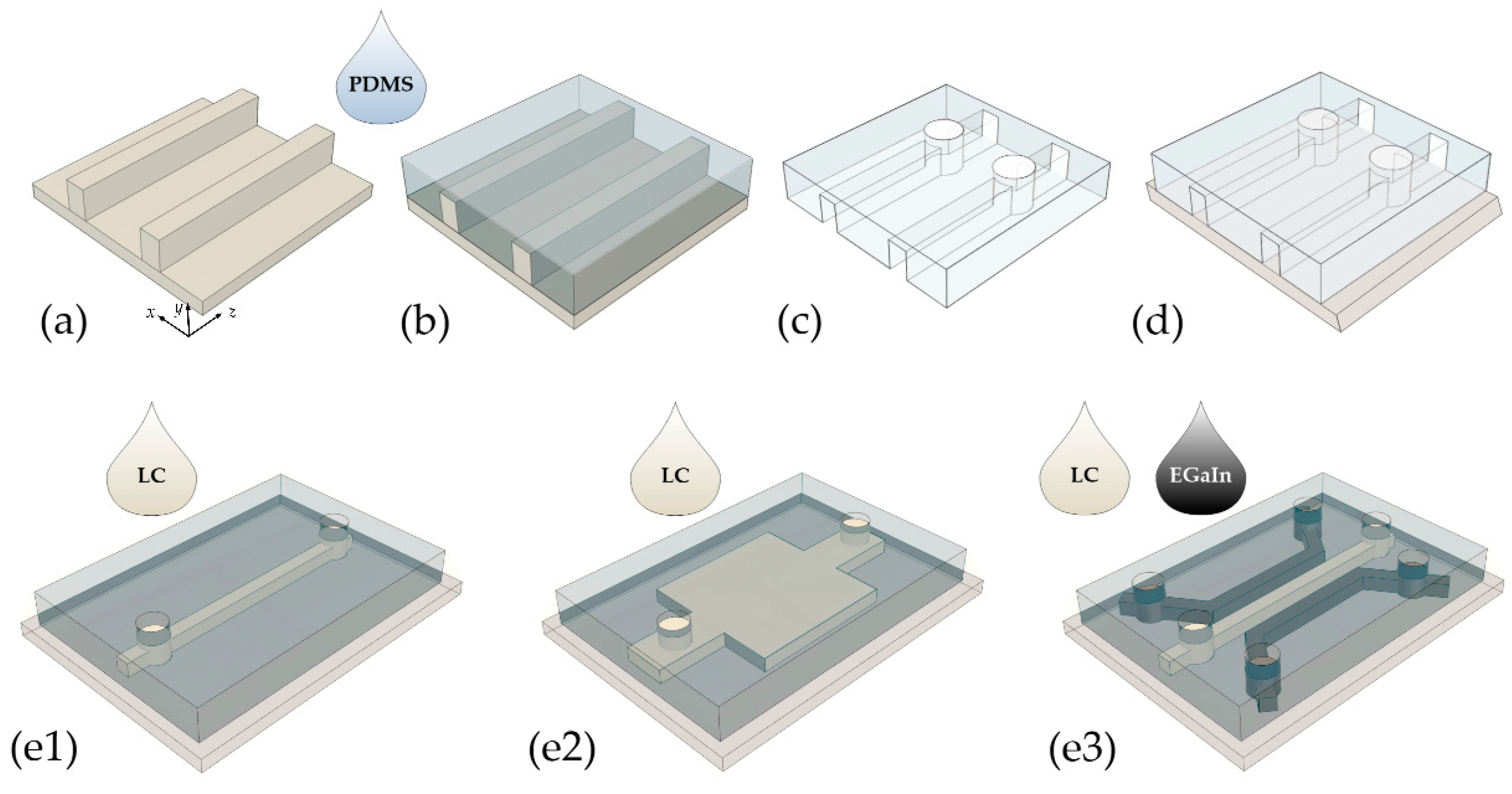
2.1. Mold Manufacturing

In this work, the LC molecular alignment within LC:PDMS structures was analyzed to check whether it is the same for molds made by three relatively simple methods (i.e., capillary film processing, 3D printing, and micromilling) and for the molds obtained in the photolithography process. Because a detailed description of low-cost fabrication techniques, including images of the molds’ textures, was presented in a previous paper [9], only the essential information is shown here.
Whatever approach is adopted, the microstructure’s design with computer-aided design (CAD) software (e.g., AutoCAD) and the fabrication of suitable masks (except for micromilling and 3D printing techniques) are the first steps to initiate the mold manufacturing processes.
A translucent film was used to create the PDMS cells of the required thickness (analogical to typical sandwich-type LC cells made of glass plates), and to obtain the microchannels in the PDMS slab. This commercially available material, also known as capillary or photostencil film, is offered in many different thicknesses down to 15 microns, depending on the supplier. Microfluidic structures with minimum widths of 50 µm are accessible with this technology, while narrower patterns tend to peel off during development. The Chromaline Super PHAT 200 film from the IKONICS Corporation was used in this work (where the number in the product name corresponds to the film thicknesses). It consists of two parts, one of which is a photographsensitive emulsion layer and the other is a polyester support. The latter allows for the attachment of an appropriate piece of capillary film to the glass substrate. The photographsensitive layer of the capillary film was exposed through a negative mask (printed on a transparency film using a high-resolution laser plotter) to UV light (100-W Analytik Jena UV light-curing lamp with a wavelength of 365 nm and an intensity of about 20 mW/cm2 for 2 min). Only the area where the mask is transparent was hardened by the UV radiation, and then the uncured capillary film was carefully washed out, leaving the convex structure of the mold. Drying the mold was the final stage of the fabrication process, taking less than 1 h in total. Our experiences showed that the master of this type is basically disposable, which is not the case for the SLA 3D printing which was also tested to obtain molds with a specific geometry. Specifically, the Form 2 desktop 3D printer with a standard clear resin (RS-F2-GCL-04) from the Formlabs Company was applied. Starting with a CAD model sent to the printer software, by optimizing the printing parameters (i.e., a single layer thickness of 25 µm and a laser spot size of about 140 µm in diameter), it was possible to produce molds with satisfactory-quality surface finish and pattern features. After a few hours of solidifying the resin layer by layer, the mold with a height of about 200 µm was cleaned with isopropyl alcohol. Using the highest possible printing resolution did not avoid the inhomogeneities of the mold structure manifested by the subsequent layers of the resin distinguished on its walls and by its upper surface roughness caused by the laser beam shape. This implies that the better quality and repeatability of the mold may be achieved by mechanical micromilling in poly(methylmethacrylate) (PMMA) material, keeping the fabrication process within a similar timeframe of several hours. For this purpose, high-precision equipment (Mini-Mill/3 from Minitech Machinery Corporation with Kyocera endmills) was used. The relevant milling conditions—including the spindle rotational speed, feed rates, and axial depths of cut—were identified in order to enhance the surfaces’ quality and obtain the micro-scale features in the PMMA mold. The main milling process was performed with the 0.5 mm diameter endmill (a feed of 500 mm/min with a step of 0.05 mm), and the final surface was processed using a 0.05 mm-diameter endmill (a feed of 500 mm/min with a step of 0.01 mm). The mold could be immediately used after cleaning from the material residue, while no burrs were visible on the sides of the drilled channels. Their walls, with the retained (and sharp) edges, were almost perpendicular to the base. The higher roughness was found at the upper surface of the mold, showing periodic unevenness related to the tool geometry, but it seems to be completely negligible in further applications. The height of the convex pattern obtained in PMMA was about 200 μm, and the mold itself could be used more than once. Completing the list of cheap and simple fabrication techniques, we come to photolithography, one of the most reliable methods in terms of mold quality. In this case, the master was made of SU-8 25 negative photoresist (Kayaku Advanced Materials, Inc., Westborough, MA, USA), providing a high-aspect ratio with nearly vertical sidewalls and superb chemical and temperature resistance. A standard process, including (i) substrate preparation (6″ silicon wafer cleaned, dried, and baked at 200 °C for 5 min on a hotplate for dehydration); (ii) SU-8 static dispension (8 mL, which gives approximately 1 mL per inch of substrate diameter); (iii) spin coating (spread cycle: ramp to 500 rpm at 100 rpm/s acceleration for 7 s; spin cycle, i.e., ramping to a spin speed of 1700 rpm at an acceleration of 300 rpm/s and holding for a total of 30 s); (iv) soft baking (on a closed hotplate at 95 °C for 6 min); (v) i-Line UV light exposure (through a 4″ square chrome mask in 1:1 contact mode with an exposure energy of 180 mJ/cm2); (vi) post-exposure baking (two-step contact hotplate process with a PEB time of 1 min at 65 °C and 6 min at 95 °C); (vii) SU-8 develop (immersion for about 3 min in a dedicated SU-8 developer to dissolve the unexposed part of the photoresist); (viii) rinsing (for about 30 s with the fresh developer); and (ix) drying (with a stream of pressurized nitrogen), resulted in a mold with a height of about 30 µm. The master could be used repeatedly to prepare the PDMS structures without compromising their quality.

2.2. LC:PDMS Structure Manufacturing

The PDMS structures were obtained by the cast-molding method (with the main steps presented in Figure 1a–d), in which the convex micropattern from the master mold was replicated in the polymer material. Different molds were used as was extensively described in the previous subsection. Each mold was cleaned with distilled water, dried with compressed air, and then placed in a plastic Petri dish (Figure 1a). The PDMS was prepared by mixing the prepolymer (SYLGARD™ 184 Silicone Elastomer Base) with the crosslinker (SYLGARD™ 184 Silicone Curing Agent), both from Dow Corning, in a weight ratio of 10:1 [18]. The prepared mixture was degassed in an extractor with a vacuum pump and then poured into a previously prepared form with a mold (Figure 1b). The PDMS was cross-linked at 75 °C for 90 min. After cross-linking, the PDMS was detached from the mold, resulting in a structure with a concave pattern (Figure 1c). The PDMS’ elastomeric property allows for the peeling off of the mold without damaging the microstructures. At this stage of the fabrication process, the elastomer sample was immersed in liquid nitrogen to drill the vertical inlets and outlets in the outermost parts of the microchannels. The next step was to permanently bond the PDMS structure to the flat substrate, i.e., either a glass plate or an additional PDMS slab (Figure 1d). In both cases, the procedure of preparing the components for their joining was identical. Firstly, the PDMS layer with a concave pattern and the support (PDMS or glass) were washed with detergent, thoroughly rinsed with distilled water, and dried with compressed air. Next, the surfaces of both layers prepared for bonding were activated with plasma (using a low-pressure Atto Plasma Cleaner from Diener Electronic) for 20 s at a reduced pressure (stabilized at 0.3 mbar) and under oxygen conditions. After removing this from the chamber, the plasma-activated elements were merged to form a complete microstructure. Its two alternatives, differing by the substrate and hereafter referred to as a PDMS:PDMS or PDMS:glass structure, respectively, were ready to be filled with liquid crystalline material. Exemplary geometries of the samples are shown in Figure 1(e1–e3).
A typical nematic liquid crystal, namely 4-cyano-4′-n-pentyl-biphenyl (5CB) and the E7 nematic liquids mixture, both commercially available from Merck, were used for the tests. Such substances’ physical and chemical parameters are well-known and widely described in the literature [46,47,48]. Liquid crystalline materials in the nematic phase (i.e., at room temperature) were injected through vertical inlets into the PDMS structure using syringes with a 0.4 mm needle.
The microchannels were filled with NLC using a syringe with a 0.4 mm needle to put a droplet into the inlet. The liquid crystal was in an anisotropic phase at a temperature of about 20 °C. The process of the structure infiltration did not consider any additional forces other than spontaneous infiltration using the capillary forces.
In order to study the electric field influence on LC molecular orientation, the LC:PDMS systems were featured with electrodes (see Figure 1(e3)) in the form of microchannels filled with the high-purity eutectic gallium–indium (EGaIn, from Sigma-Aldrich). This electrically conductive fluid metal (with a resistivity of 29.4 × 10⁻⁶ Ω·cm) comprises 75.5% gallium and 24.5% indium by weight. Its low viscosity and rheological properties at room temperature allow for the formation of metal electrodes within the microchannels with adequate cross-sectional dimensions [49].

2.3. Optical Measurements and Observations

A digital microscope (KEYENCE VHX 5000) with a universal zoom lens VH-Z20 (20–200×) and a long-working-distance, high-performance zoom lens VH-Z50 (50–500×) was used for the observations, dimensional measurements, and the capturing of high-resolution images (1600 × 1200 pixels in the standard and 4800 × 3600 pixels in the stitching mode). The LED transmitted lighting could be used in conjunction with reflected illumination from the lens. The light from each source can be adjusted independently, making it possible to perform observations with an optimum balance of light intensity. The polarization observation setup included in the system allowed for standard polarizing microscope (POM) measurements with white light transmitted through the sample placed between crossed polarizers (see Figure 2m). In addition, a polarization optical microscope (Zeiss Jenalab POL) with a Bertrand lens (introduced between the analyzer and the ocular) was used to obtain the conoscopic images in the PDMS:PDMS cells. The conoscopic technique helps to identify the exact nature of the surface anchoring in the LC samples.

3. Results

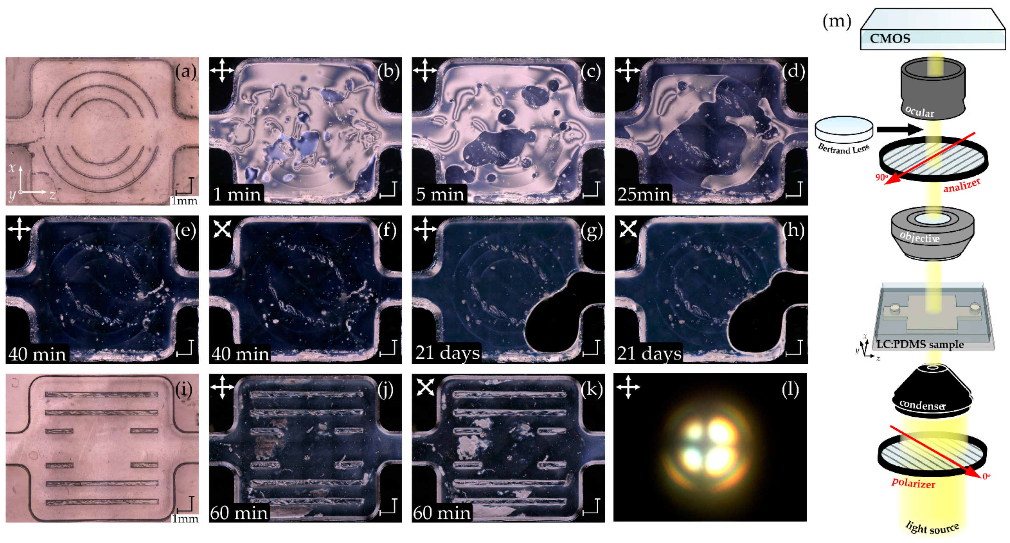
3.1. PDMS:PDMS Cells with Different Liquid Crystalline Materials

The initial stage of the experimental studies was devoted to the confirmation of the NLC molecular alignment at the PDMS surfaces. For this purpose, the PDMS:PDMS cells were assembled in an analogical way, as is carried out in the typical glass-plate-based LC cells used for the testing of liquid crystalline components and materials. Due to the elasticity of the host material and the possibility of the entire structure collapsing, several types of cells with sub-pillars of different shapes were designed. Additionally, the pillars prevented any change in the cell gap over its total area. The molds for these PDMS:PDMS structures were made using a UV-cured photostencil film of the thickness of 200 µm. Two exemplary empty cells with concentric semi-circular and rectangular sub-pillars are shown in Figure 2a,i, respectively. Many other geometries were also tested, giving no evidence of the sub-pillars’ influence on long-distance ordering. The dimensions of the central part of the structure were approximately 9.3 × 9.3 mm. The photographs do not show the two side channels with inlet/outlet holes to provide liquid crystalline material. The PDMS:PDMS cell from Figure 2a was filled with a 5CB nematic liquid crystal at a temperature of about 20 °C. This anisotropic liquid enters the cell almost spontaneously, filling up its entire volume of about 17 µL in 10 s (see Figure 2b). The chronological changes in the molecular orientation for 5CB NLC, visualized by the polarizing microscope (POM) images, are presented sequentially in Figure 2b–h. The time elapsed since complete infiltration of the LC cell and the angular orientation of the polarizer and analyzer axes are indicated in each photo. It is worth noting that the initial flow-induced perturbed planar molecular arrangement, with disclination points and lines (Figure 2b–d), was eventually transformed into the homogenous one (see Figure 2e,f) taken 40 min after infiltration). The light transmittance in the central cell area (and in the middle of the side channels) is at the same minimal level for the LC cell edge aligned at any angle to the crossed-polarizer axis. Moreover, for the specific angular positions of the cell, i.e., at 0 degrees (Figure 2e) and 45 degrees (Figure 2f), the minimal and maximal light transmittance in the close vicinity of the cell walls were obtained, respectively. Some defects in the structures (mainly related to the irregularities in the mold surfaces) did not influence the test results. The observations confirmed the homeotropic (vertical) alignment of 5CB NLC molecules in the PDMS:PDMS cell. It was then checked every few days over a long time. Pictures of the same sample infiltrated with 5CB NLC taken after 21 days (Figure 2f,g) proved the maintenance of the molecular orientation despite the leakage of LC material from the cell. Analogical experimental work was performed on the PDMS:PDMS cell with rectangular pillars (Figure 2i) filled with E7 nematic liquid crystal mixture. The final molecular arrangement was established about 1 h after the infiltration (Figure 2j,k). However, the vanishing boundaries between different regions with the flow-induced and the pillar-forced orientation could be identified until that time. Eventually, vertical alignment on the PDMS surfaces was achieved, leading to the homeotropic arrangement in the entire PDMS:PDMS cell volume. The latter finding was confirmed by the conoscopic examination of the central part of the PDMS:PDMS cells with the exemplary image presented in Figure 2l. The cross arms were parallel to the polarizers’ axes, and remained unchanged when rotating the sample on the microscope stage.

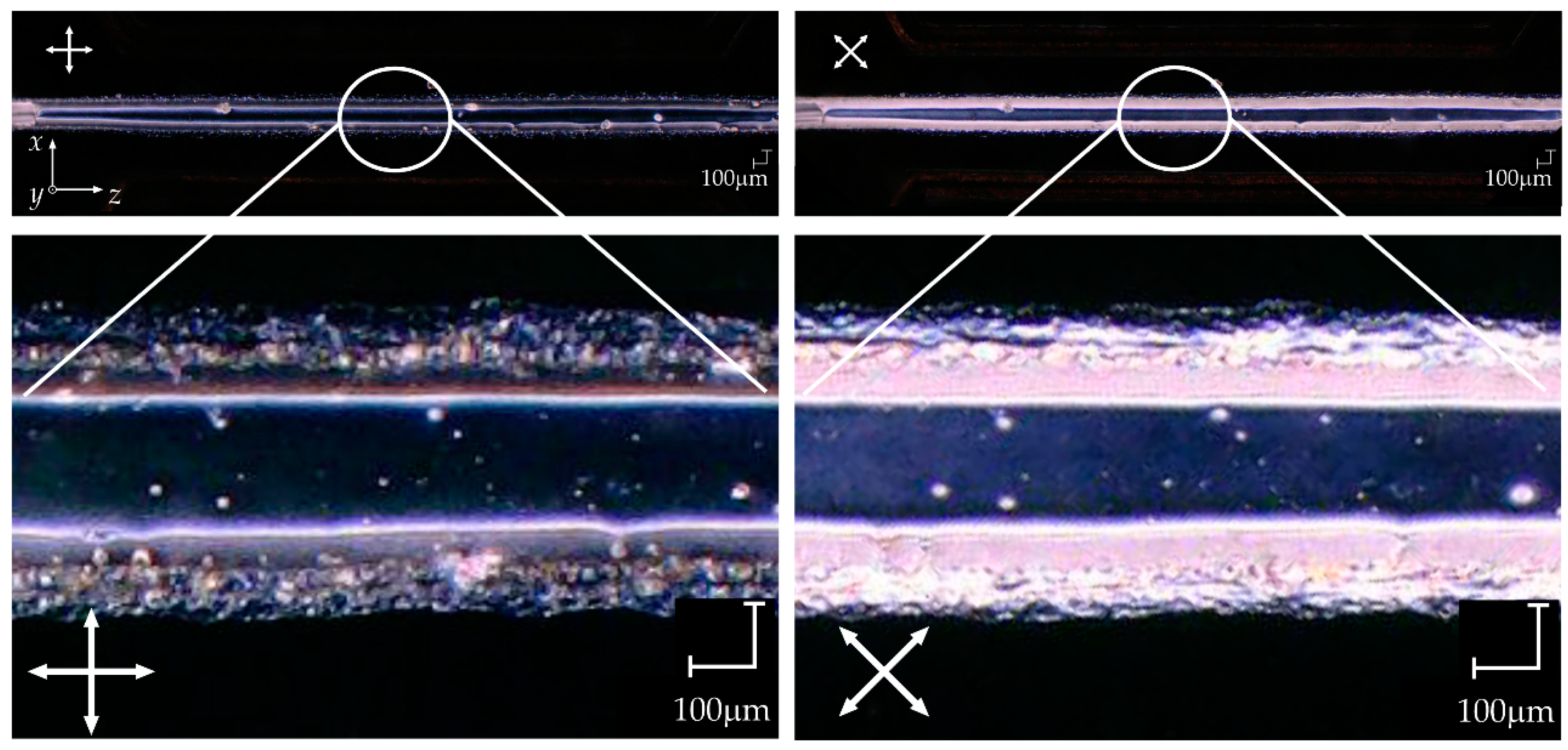
3.2. LC Orientation in PDMS:PDMS and PDMS:Glass Microstructures
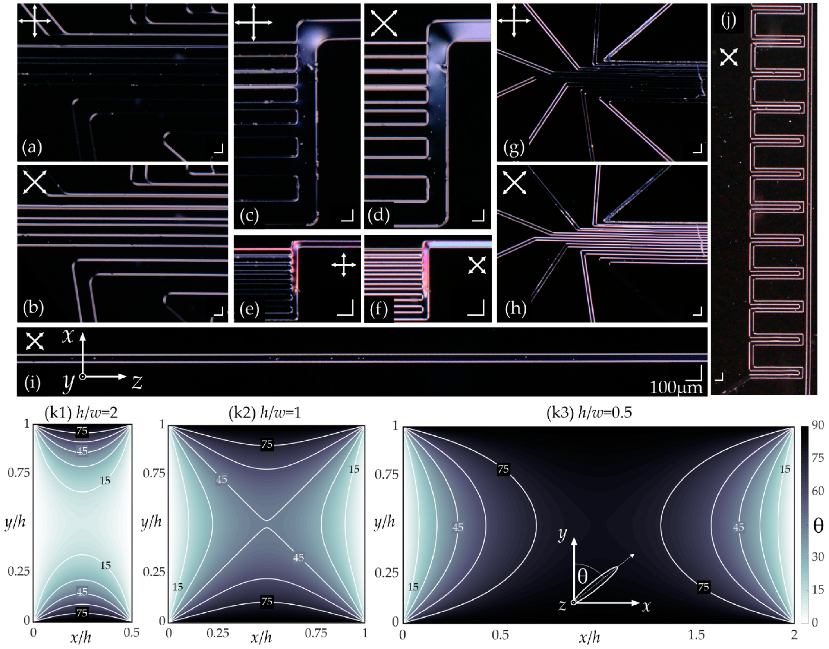
After confirming the vertical alignment (VA) of the NLCs on the PDMS surfaces in the bulk cells, further experimental tests were performed to study the LC molecular orientation depending on the molds used to fabricate the PDMS:PDMS and PDMS:glass microstructures. The names of the technologies applied for the molds’ fabrication are used as the subsubsections. With no significant differences in observations for the various liquid crystalline materials examined therein, the results for only one of them are reported below. If it is not explicitly denied, the results were obtained regardless of the LC material applied.
It is worth noting that a planar orientation (with long molecules’ axes ordered along the canal axes) was achieved in the initial phase of the infiltration process. Such a flow-induced molecular arrangement was then eventually changed if the VA on the PDMS surfaces became dominant.

3.2.1. 3D Printing

Despite our previous tests indicating the roughness of the SLA 3D-printed molds [9], studies on the LC molecular orientation were undertaken due to this fabrication method’s simplicity. The 3D printing can be performed apart from additional equipment or initial preparations. The process does not require mask fabrication, precise equipment operation, or access to sophisticated laboratory facilities. Specifically, a microchannel structure with a cross-section of 200 × 200 μm was designed. Due to the type of resin applied, the mold was slightly deformed in the areas between the channels. Moreover, the structure measurements confirmed the increased dimensions of the microchannels to 240–260 µm in width. After about 5 min from infiltration (with the volumetric flow rate varying in the range of 0.7–1.8 µL/min), the orientation of the E7 NLC molecules was as shown in Figure 3a,b along the entire length of the 10-mm-long microchannel in the PDMS:PDMS structure. The area where the molecules could be oriented perpendicularly to the bottom layer of the PDMS channel was relatively narrow. This is related to the value of the channel aspect ratio (high/width, h/w) being close to one for which the anchoring contribution from the side walls matched up to the contribution from the top surface (please refer to the results of the numerical simulations shown in Figure 6(k1–k3) for guidance). Nevertheless, the firmly rounded edges on the upper part of the channel and the inclinations of highly imperfect sidewalls towards the substrate plane did not allow a perfect VA alignment at the PDMS-LC intersections. The polarizing optical micrographs in Figure 3a,b show high irregularities in the molecular arrangement obtained in the channel. In addition, the orientation became totally random three days after infiltration, which was manifested by the scattering of light by the defects and spatial variation in the transmitted light intensity (see Figure 3c). Replacing the substrate with a glass plate did not change the quality of the LC molecular arrangement.

3.2.2. Micromilling in PMMA

Our previous research showed that micromilling in PMMA might be an accurate method to obtain molds with suitable geometrical parameters [9]. Particular attention should be paid to the undistorted sidewalls, which are almost perfectly perpendicular to the base surface. Another advantage is the potential to create complex structures. One of the many tested approaches was the trial samples with five different channels fabricated on both PDMS and glass substrates. The channels’ widths were 50, 100, 150, 200, and 250 µm, respectively (see Figure 4a). Two perpendicular channels were used as interconnectors, and the full structure was terminated with four openings (not shown in the photo). This arrangement ensured the air-bubble-free infiltration of the entire length of the channels tested. The photographs in Figure 4 were taken for the whole structure filled with E7 NLC, and when the flow of the liquid crystalline material was terminated. Upon the closer examination of the POM images at 0 and 45 degree angles to the polarizers’ axes, discontinuities in the LC orientation with the disclination points were visible. This was particularly emphasized in the vicinity of the channels’ interconnectors. Moreover, the segments with different molecular arrangements along the channels could be distinguished. Identical orientation along the entire length of the channels was not achieved. This conclusion was reached for both the PDMS:PDMS (Figure 4a–f) and PDMS:glass (Figure 4g,h) structures of the leader type. Specifically, the POM image of the molecular orientation escape in a microchannel with the aspect ratio equal to one, resulting in a single singularity at the channel center, is shown in Figure 4e,f. It is worth underlining that the microchannel itself is of much better quality than that described in the Section 3.2.1 (please see the photographs in Figure 3a,b for comparison), indicating a much better quality of the micromilled mold. The higher integer singularities were also observed in this channel due to the same tendency of the molecules to orient orthogonally to the sidewalls and to the top wall. The design of the sample with a single channel was also tested to resolve whether the above observations were not the result of the structure’s geometry and complexity. In particular, a 200-µm-wide microchannel made in the PDMS:glass architecture was studied. After the channel infiltration (with the volumetric flow rate in the range of about 1.5–4.0 µL/min), a consistent orientation along the entire length of the channel was eventually achieved. Figure 4i,j shows polarizing optical micrographs of the equilibrium orientation of the LC molecules, which can be perturbated by the flow. Unfortunately, a complete lack of molecular alignment was observed a few days after the filling of the structure (see Figure 4k).

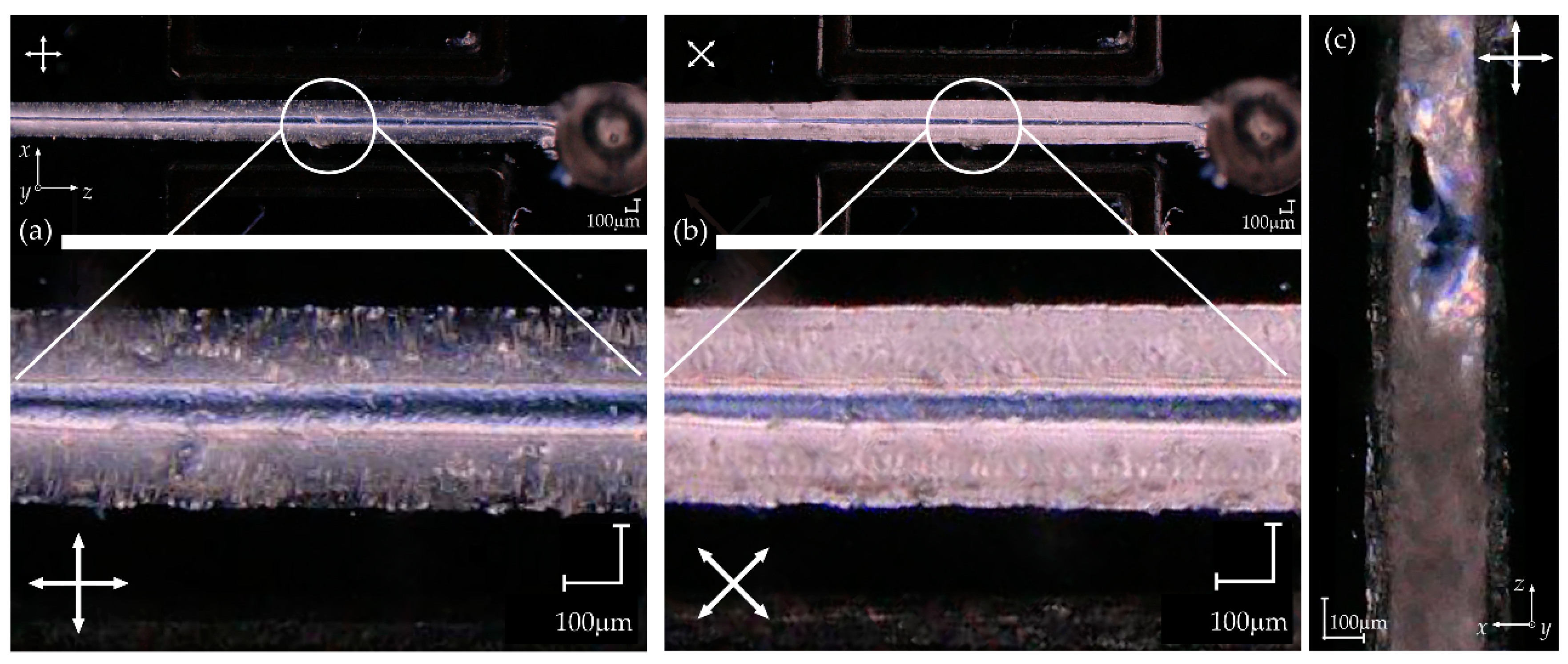
3.2.3. UV-Cured Photostencil Film Processing

UV-cured photostencil film processing was the last non-photolithographic technique of mold fabrication to be tested for its ability of LC molecular alignment in the microchannels. The microchannel to be tested in the PDMS:glass architecture was designed to be 200 µm high and 200 µm wide. A much wider channel with a flat top but highly distorted sidewalls was achieved. After putting the LC material into the inlet, the planar molecular alignment was initially achieved for the volumetric flow rate varying in the range of 0.6–1.8 µL/min. Although material imperfections were visible near the sidewalls of the channels, the homeotropic alignment in the central part of the channel was achieved after 5 min from infiltration with E7 NLC. This observation may be confirmed by the photographs shown in Figure 5. Analogical results were obtained in the PDMS:PDMS structure when the PDMS layer was used as the substrate in place of the glass plate. The molecular orientation in the microchannels fabricated using the UV-cured photostencil film remained stable for days.

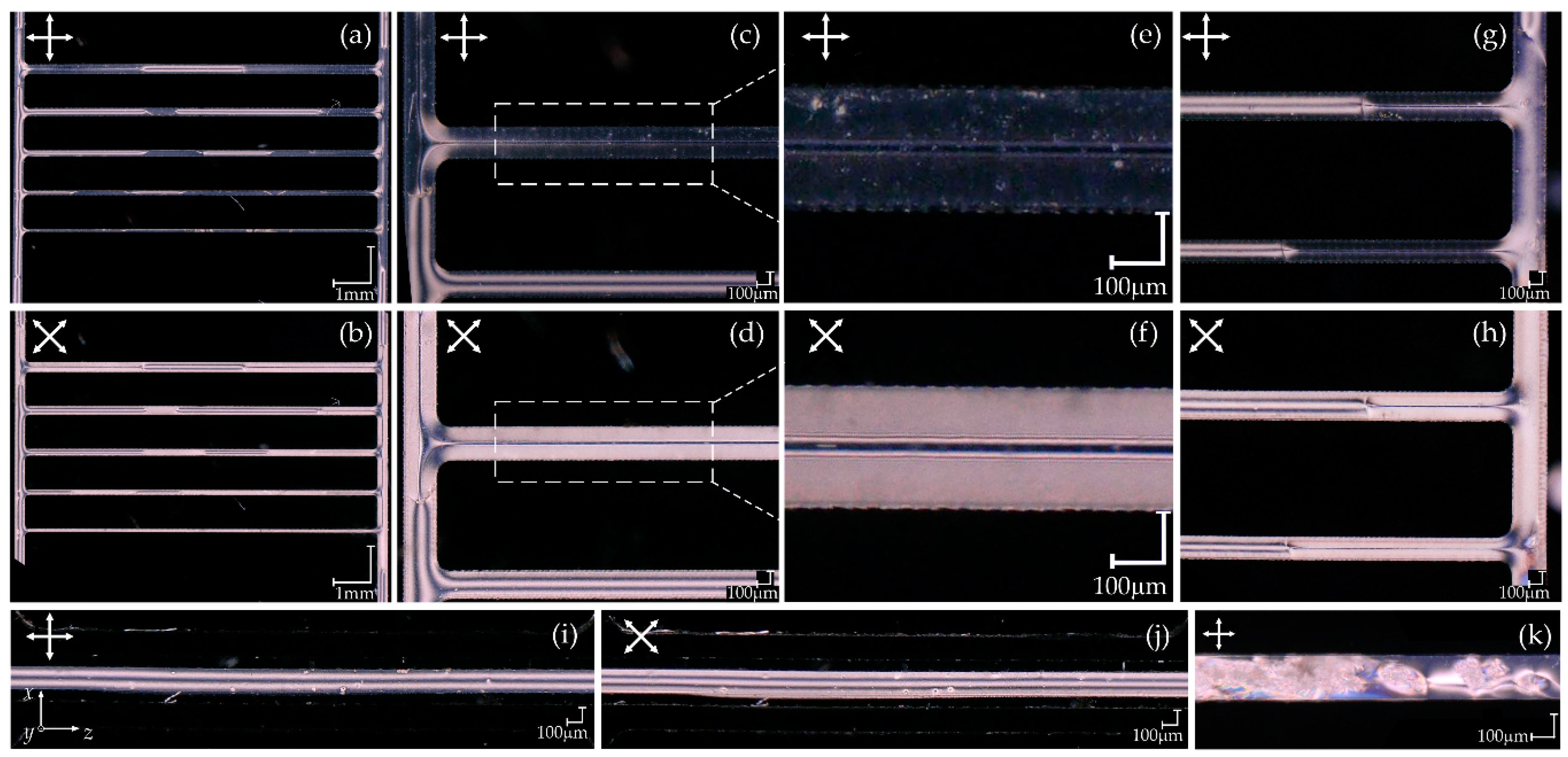
3.2.4. Photolithography with the Use of SU-8 Negative Photoresist

The final phase of the studies to evaluate the ways in which the mold manufacturing technology affects the orientation of the liquid crystal molecules within PDMS microstructures was to analyze the structures made from the SU-8 master. As was already mentioned, homeotropic alignment in PDMS microstructures, obtained thanks to the photolithographic processing of the mold, has been widely reported in the literature. A particular structure containing eight microchannels of different widths—20, 30, 40, 50, 100, 150, 200, and 250 µm—was created (see Figure 6a–d) to validate these reports. Due to the parameters of the technological processes, the height of the structures made of photoresist on the silicon wafer was about 30 µm. All of the channels were merged with one entrance channel (see, e.g., Figure 6c) and terminated with radially distributed output channels (see, e.g., Figure 6h). The in/outlets were drilled at the beginning/end of each 200-µm-wide in/outflow channel, respectively. Such a design allowed us to get rid of the air bubbles during the infiltration with liquid crystalline material, and to better separate the channels from each other. Having each channel end with its independent outlet should minimize the flow and orientation issues occurring in the ladder-like-shaped structure from Figure 4. The PDMS:glass was filled with 5CB NLC at 20 °C. A slightly different time was required for each channel to be infiltrated entirely with the anisotropic liquid. This is mainly due to differences in the widths and lengths of the individual microchannels. Specifically, the microchannels’ lengths vary from 28 to 30 mm in the central part of the structure where the channels are parallel to each other. The volumetric flow rate between 3 to 30 nl/min was estimated depending on the channel width. The photographs shown in Figure 6a–d were taken about 5 min after introducing the liquid crystalline material to the inlet. Even if flow-induced orientation is still visible within the entrance channel (Figure 6c,d), the molecular alignment is completely established in the tested channels. It is enough to provide the POM images of the two outer sections of the structure because the molecular ordering was unchanged along the whole length of the straight channels. The homeotropic alignment in the central part of the channels’ widths, resulting from the pronounced VA on the top surfaces, is clearly recognizable for the microchannels wider than 40 µm. When the aspect ratio (h/w) increases to more than one (for the narrower channels), the LC alignment on the sidewalls determines the molecular orientation in the channel cross-section. It is clearly visible when analyzing the results of the numerical simulations presented in Figure 6(k1–k3). The latter represents the molecular arrangement inside the waveguide channels, and was determined using a finite-difference relaxation scheme with an assumption of the stiff homeotropic boundary conditions on the PDMS surfaces. The numerical procedure was the same as described in [43]. The perfect VA alignment at all of the PDMS-LC intersections, including the top surfaces and sidewalls of the microchannels, was also proven in an analogical test sample consisting of channels with widths of 10, 20, 25, 30, 35, 40, 45, and 50 µm (Figure 6e–h). This is why the channels are barely visible when aligned along the polarizers’ axes, and the maximum intensity of the transmitted light in the vicinity of the channels’ sidewalls is obtained after rotating the sample by 45 degrees. Additional tests were performed in the PDMS:PDMS system with 50-µm-wide channels of simple (Figure 6i) and more complex (Figure 6j) geometry infiltrated with 5CB NLC. As was previously found, they led to the conclusion that NLC molecules are perfectly vertically aligned on the surfaces inside the PDMS microstructure made from the SU-8 mold. The homeotropic anchoring on the channel walls was found to be stable in time.

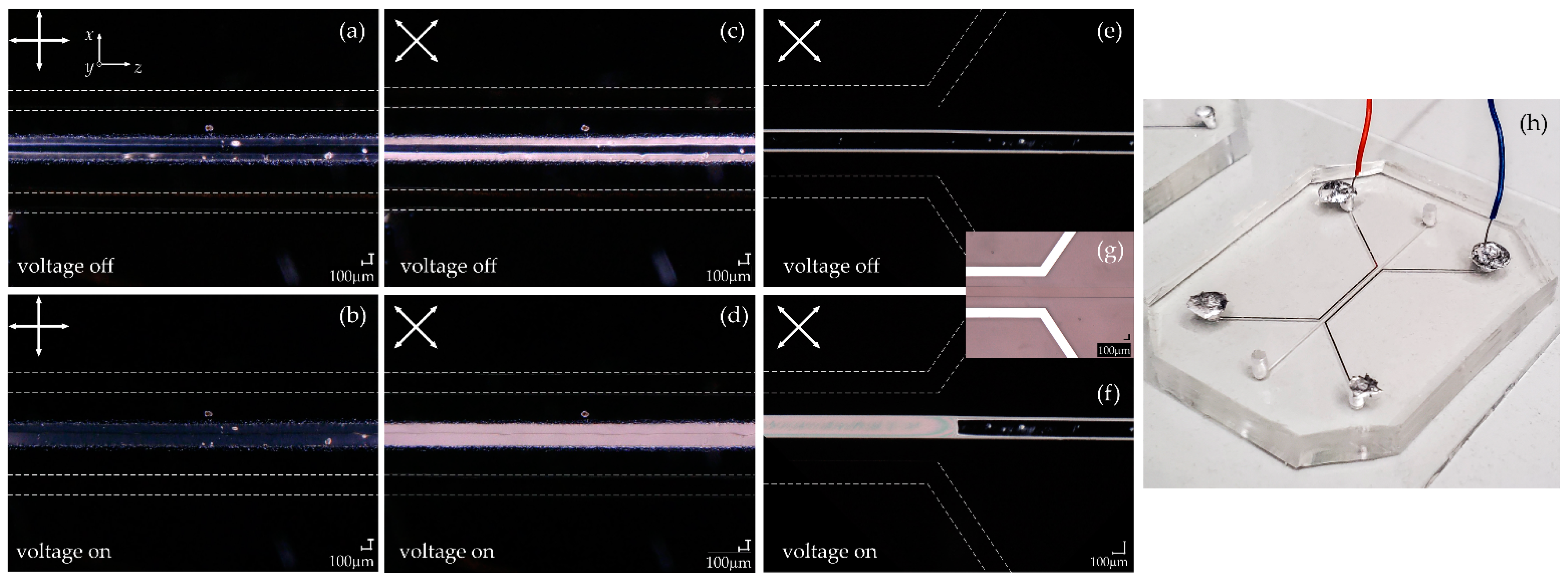
3.3. Change in the Molecular Alignment with the Use of an Electric Field

Eventually, studies on the efficient reorientation of the liquid crystal molecules under the influence of an external electric field were performed. For this purpose, the micropattern with three channels (see Figure 7h)—the central one (to be filled with LC) and two side channels (to be injected with metal eutectic Ga-In)—was replicated in PDMS using two molds made of the Chromaline Super PHAT 200 photostencil film and SU-8 photoresist, respectively. The width of each channel was designed to be 200 µm, as was the distance between them. In the case of the first technology, the manufacture of the mold is not so precise, and the main channel was again wider than anticipated. Depending on the mold used for fabrication, the height of the microchannels was about 200 µm and 30 µm, respectively. Both structures were made by bonding the PDMS layer to the glass substrate. The side channels (with the length of 10 mm for the section parallel to the main channel with the liquid crystalline material) were infiltrated with the eutectic gallium–indium using a syringe with a specially prepared needle. A sinusoidal alternating voltage (at the frequency of 1 kHz) was applied to the microstructured electrodes. At the peak-to-peak voltages of 300 V and 150 V, the complete reorientation of the E7 and 5CB NLC molecules (with their long axes aligned with the direction of the electric field) was observed in the first (UV-cured photostencil film) and the second (SU-8) structure, respectively. The electrically-driven change in a molecular arrangement is shown in the POM images given in Figure 7a–f. This effect is particularly evident in the case shown in Figure 7f, where an initial part of the structure is presented with the electrode feeder channel just approaching the main channel. Two regions of entirely different molecular orientation (i.e., homeotropic and planar) were achieved. The disagreements in the voltages applied in both cases (i.e., for structures fabricated using different molds) may be related to the geometrical differences (the different dimensions and aspect ratios of the channels) and unidentical physical properties of the liquid crystal materials (e.g., different elastic constants and electric permittivities). However, only qualitative observations of the changes in the orientation of the liquid crystal molecules under the influence of an electric field were aimed for in this phase of the studies.

4. Discussion and Conclusions

The fabrication of the master mold is undoubtedly the most expensive stage of the cast-molding technique applied for the PDMS-based microstructures’ replication. In photonic systems for which high geometrical resolution is required, photolithography is still preferably used to obtain the best-quality master mold. Such financial investment is particularly uneconomic when new microstructures are designed and pre-tested. In fact, in the initial stage of the development, the better option is to test microdevices fabricated using rapid and cheap technologies with readily accessible materials. Therefore, time-consuming and expensive processes utilizing sophisticated cleanroom facilities and complex technological procedures may be avoided. However, this is only reasonable if all of the cases lead to qualitatively consistent results. In this work, LC:PDMS structures obtained using different technologies were tested for the possibility of obtaining a stable alignment of liquid crystal molecules. A summary of the applicability of the fabrication methods may be found by analyzing the data presented in Table 1. Please note that all of the parameters and descriptions refer exclusively to the structures of the type described in this paper. Some quantitative parameters, such as the deviation of the final PDMS channel width from the assumed one (in the design) and typical size deviations (estimated as the standard deviation from the mean value for many samples of the same type) for a 200-μm-wide channel have been selected, among others, for the benchmarking. When comparing the possible most-diminutive individual mold dimensions (width/height/channels separation), the entire fabrication procedure (with all its subprocesses) must be considered. For example, the process of washing away the uncured material is essential when a capillary film is used for the mold. This may lead to the unwanted damage of the mold or its resizing. Moreover, particular attention has to be devoted to the implementation of the perfect dose of UV light when exposing the film to obtain the channels of the required geometry. In the case of SLA 3D printing, the mold size is greatly affected by the excess resin that solidifies throughout the process, generally widening the channels. This is especially noticeable when the designed separation between the channels is too small. Eventually, the target sizes of PMMA molds are highly dependent on the endmills used. As far as the quality of the LC molecular arrangement obtained in the studied structures is concerned, it should be remembered that each mold fabrication method is characterized by its technology and the material applied, which significantly affects the final surface roughness of the mold. This has been concluded as one of the critical parameters promoting the uniform and stable alignment of liquid crystal molecules. SLA 3D printing and micro-milling were found to be inefficient for this purpose. The molecule anchoring was disrupted, making it hard to determine the LC molecular orientation accurately. Moreover, the appearance of some defects in molecular arrangement when using the samples has been observed. It seems that the application of the photostencil film is straightforward and cheap, which makes it a rapid prototyping method. This allowed for the homeotropic alignment in the center of LC:PDMS channels to be obtained with the LC molecular arrangement being stable in time. However, only relatively simple patterns may be designed, with the lowest possible dimensions of the geometrical features of the sample being far from acceptable for use in optical system applications.
Taking the above into account, one can say that our manuscript contributes to a better understanding of the LC:PDMS operation, and our studies allow for the further optimization of such structures. Nevertheless, photolithography remains unquestionably the best technique for producing the best quality LC:PDMS structures. With the appropriate parameters of SU-8 development and the UV irradiation dose, the transversal dimensions of the mold channels may go down to single micrometers. More detailed results showing the designs made in SU-8 with sizes suitable for light guidance, and with electrodes of more complex shape, are presented elsewhere. The latter was made possible by using the novel approach for electrode fabrication presented in this paper. We believe that it is a first step for the creation of low-cost, high-optical-quality, electrically-driven photonic devices (with no need for LC alignment treatment).

Author Contributions

Conceptualization, K.A.R.; methodology, K.A.R., A.D. and M.J.; investigation, S.B., P.S., K.M. and M.S.; data curation, S.B.; writing—original draft preparation, S.B. and K.A.R.; writing—review and editing, K.A.R. and A.D.; visualization, S.B. and K.A.R.; supervision, K.A.R.; project administration, K.A.R.; funding acquisition, K.A.R. All authors have read and agreed to the published version of the manuscript.

Funding

The studies were funded by the FOTECH-1 project “Electrically-driven waveguiding systems in LC:PDMS structures” granted by the Warsaw University of Technology under the Excellence Initiative: Research University (ID-UB) program.

Conflicts of Interest

The authors declare no conflict of interest.

References

  1. Cho, S.H.; Godin, J.; Chen, C.H.; Tsai, F.S.; Lo, Y.-H. Microfluidic photonic integrated circuits. Optoelectron. Mater. Devices 2008, 7135, 71350M. [Google Scholar]
  2. Rodríguez-Ruiz, I.; Ackermann, T.N.; Muñoz-Berbel, X.; Llobera, A. Photonic lab-on-a-chip: Integration of optical spectroscopy in microfluidic systems. Anal. Chem. 2016, 88, 6630–6637. [Google Scholar] [CrossRef] [PubMed] [Green Version]
  3. Manz, A.; Graber, N.; Widmer, H.M. Miniaturized total chemical analysis systems: A novel concept for chemical sensing. Sens. Actuators B Chem. 1990, 1, 244–248. [Google Scholar] [CrossRef]
  4. DeMello, A.J. Control and detection of chemical reactions in microfluidic systems. Nature 2006, 442, 394–402. [Google Scholar] [CrossRef] [PubMed]
  5. Jung, W.; Han, J.; Choi, J.-W.; Ahn, C.H. Point-of-care testing (POCT) diagnostic systems using microfluidic lab-on-a-chip technologies. Microelectron. Eng. 2015, 132, 46–57. [Google Scholar] [CrossRef]
  6. Lim, J.-G.; Lee, S.-S.; Lee, K.-D. Polymeric arrayed waveguide grating using imprint method incorporating a flexible PDMS stamp. Opt. Commun. 2007, 272, 97–101. [Google Scholar] [CrossRef]
  7. Ku, K.; Hisano, K.; Kimura, S.; Shigeyama, T.; Akamatsu, N.; Shishido, A.; Tsutsumi, O. Environmentally Stable Chiral-Nematic Liquid-Crystal Elastomers with Mechano-Optical Properties. Appl. Sci. 2021, 11, 5037. [Google Scholar] [CrossRef]
  8. Zhou, Z.; Chen, D.; Wang, X.; Jiang, J. Milling positive master for polydimethylsiloxane microfluidic devices: The microfabrication and roughness issues. Micromachines 2017, 8, 287. [Google Scholar] [CrossRef] [Green Version]
  9. Baczyński, S.; Sobotka, P.; Marchlewicz, K.; Dybko, A.; Rutkowska, K. Low-cost, widespread and reproducible mold fabrication technique for PDMS-based microfluidic photonic systems. Photonics Lett. Pol. 2020, 12, 22–24. [Google Scholar] [CrossRef]
  10. Korkmaz, E.; Onler, R.; Ozdoganlar, O.B. Micromilling of poly (methyl methacrylate, PMMA) using single-crystal diamond tools. Procedia Manuf. 2017, 10, 683–693. [Google Scholar] [CrossRef]
  11. Comina, G.; Suska, A.; Filippini, D. PDMS lab-on-a-chip fabrication using 3D printed templates. Lab. A Chip 2014, 14, 424–430. [Google Scholar] [CrossRef] [PubMed]
  12. Kaigala, G.V.; Ho, S.; Penterman, R.; Backhouse, C.J. Rapid prototyping of microfluidic devices with a wax printer. Lab. A Chip 2007, 7, 384–387. [Google Scholar] [CrossRef]
  13. Grimes, A.; Breslauer, D.N.; Long, M.; Pegan, J.; Lee, L.P.; Khine, M. Shrinky-Dink microfluidics: Rapid generation of deep and rounded patterns. Lab. A Chip 2008, 8, 170–172. [Google Scholar] [CrossRef] [Green Version]
  14. Chudy, M.; Grabowska, I.; Ciosek, P.; Filipowicz-Szymanska, A.; Stadnik, D.; Wyzkiewicz, I.; Jedrych, E.; Juchniewicz, M.; Skolimowski, M.; Ziolkowska, K. Miniaturized tools and devices for bioanalytical applications: An overview. Anal. Bioanal. Chem. 2009, 395, 647–668. [Google Scholar] [CrossRef]
  15. Masrie, M.; Majlis, B.Y.; Yunas, J. Experimental analysis on SU8-micromolding structure of PDMS (poly-dimethylsiloxane) based microfluidic channel. IEEE Int. Conf. Semicond. Electron. 2014, 115–118. [Google Scholar] [CrossRef]
  16. Behroodi, E.; Latifi, H.; Bagheri, Z.; Ermis, E.; Roshani, S.; Moghaddam, M.S. A combined 3D printing/CNC micro-milling method to fabricate a large-scale microfluidic device with the small size 3D architectures: An application for tumor spheroid production. Sci. Rep. 2020, 10, 1–14. [Google Scholar]
  17. Villegas, M.; Cetinic, Z.; Shakeri, A.; Didar, T.F. Fabricating smooth PDMS microfluidic channels from low-resolution 3D printed molds using an omniphobic lubricant-infused coating. Anal. Chim. Acta 2018, 1000, 248–255. [Google Scholar] [CrossRef] [PubMed]
  18. SYLGARD™ 184 Silicone Elastomer Kit Technical Data Sheet. Available online: https://www.dow.com/en-us/document-viewer.html?ramdomVar=6555882543077060701&docPath=/content/dam/dcc/documents/en-us/productdatasheet/11/11-31/11-3184-sylgard-184-elastomer.pdf (accessed on 18 July 2021).
  19. Stankova, N.E.; Atanasov, P.A.; Nikov, R.G.; Nikov, R.G.; Nedyalkov, N.N.; Stoyanchov, T.R.; Fukata, N.; Kolev, K.N.; Valova, E.I.; Georgieva, J.S. Optical properties of polydimethylsiloxane (PDMS) during nanosecond laser processing. Appl. Surf. Sci. 2016, 374, 96–103. [Google Scholar] [CrossRef]
  20. Testa, G.; Persichetti, G.; Sarro, P.M.; Bernini, R. A hybrid silicon-PDMS optofluidic platform for sensing applications. Biomed. Opt. Express 2014, 5, 417–426. [Google Scholar] [CrossRef] [Green Version]
  21. Schneider, F.; Draheim, J.; Kamberger, R.; Wallrabe, U. Process and material properties of polydimethylsiloxane (PDMS) for Optical MEMS. Sens. Actuators A Phys. 2009, 151, 95–99. [Google Scholar] [CrossRef]
  22. Shih, T.-K.; Chen, C.-F.; Ho, J.-R.; Chuang, F.-T. Fabrication of PDMS (polydimethylsiloxane) microlens and diffuser using replica molding. Microelectron. Eng. 2006, 83, 2499–2503. [Google Scholar] [CrossRef]
  23. Song, W.; Vasdekis, A.E.; Li, Z.; Psaltis, D. Low-order distributed feedback optofluidic dye laser with reduced threshold. Appl. Phys. Lett. 2009, 94, 051117. [Google Scholar] [CrossRef] [Green Version]
  24. Chung, A.J.; Erickson, D. Optofluidic waveguides for reconfigurable photonic systems. Opt. Express 2011, 19, 8602–8609. [Google Scholar] [CrossRef] [PubMed] [Green Version]
  25. Na, Y.J.; Yoon, T.Y.; Park, S.; Lee, B.; Lee, S.D. Electrically programmable nematofluidics with a high level of selectivity in a hierarchically branched architecture. ChemPhysChem 2010, 11, 101–104. [Google Scholar] [CrossRef] [PubMed]
  26. Schmidtke, J.; Terentjev, E.M. Polydimethylsiloxane-enclosed liquid crystal lasers for lab-on-chip applications. Appl. Phys. Lett. 2010, 96, 151111. [Google Scholar] [CrossRef]
  27. Wang, I.T.; Lee, Y.-H.; Chuang, E.-Y.; Hsiao, Y.-C. Sensitive, color-indicating and labeling-free multi-detection cholesteric liquid crystal biosensing chips for detecting albumin. Polymers 2021, 13, 1463. [Google Scholar] [CrossRef]
  28. Cuennet, J.G.; Vasdekis, A.E.; De Sio, L.; Psaltis, D. Optofluidic modulator based on peristaltic nematogen microflows. Nat. Photonics 2011, 5, 234–238. [Google Scholar] [CrossRef]
  29. Wee, D.; Hwang, S.H.; Song, Y.S.; Youn, J.R. Tunable optofluidic birefringent lens. Soft Matter 2016, 12, 3868–3876. [Google Scholar] [CrossRef]
  30. Pan, J.; Liu, S.; Yang, Y.; Lu, J. A highly sensitive resistive pressure sensor based on a carbon nanotube-liquid crystal-PDMS composite. Nanomaterials 2018, 8, 413. [Google Scholar] [CrossRef] [Green Version]
  31. d’Alessandro, A.; Asquini, R.; Chiccoli, C.; Martini, L.; Pasini, P.; Zannoni, C. Liquid crystal channel waveguides: A Monte Carlo investigation of the ordering. Mol. Cryst. Liq. Cryst. 2015, 619, 42–48. [Google Scholar] [CrossRef]
  32. Asquini, R.; Chiccoli, C.; d’Alessandro, A.; Pasini, P.; Zannoni, C. Monte Carlo Study of Slot-waveguide Liquid Crystal Phase Shifters. Mol. Cryst. Liq. Cryst. 2019, 683, 46–55. [Google Scholar] [CrossRef]
  33. Asquini, R.; Chiccoli, C.; Pasini, P.; Civita, L.; d’Alessandro, A. Low power photonic devices based on electrically controlled nematic liquid crystals embedded in poly (dimethylsiloxane). Liq. Cryst. 2018, 45, 2174–2183. [Google Scholar] [CrossRef]
  34. d’Alessandro, A.; Martini, L.; Civita, L.; Beccherelli, R.; Asquini, R. Liquid crystal waveguide technologies for a new generation of low-power photonic integrated circuits. Proc. SPIE 2015, 9384, 93840L. [Google Scholar]
  35. Asquini, R.; Martini, L.; d’Alessandro, A. Fabrication and characterization of liquid crystal waveguides in PDMS channels for optofluidic applications. Mol. Cryst. Liq. Cryst. 2015, 614, 11–19. [Google Scholar] [CrossRef]
  36. Civita, L.; Quaranta, S.; Asquini, R.; d’Alessandro, A. Design of a Multi Mode Interferometer using LC: PDMS technology. Mol. Cryst. Liq. Cryst. 2019, 684, 58–65. [Google Scholar] [CrossRef]
  37. d’Alessandro, A.; Civita, L.; Asquini, R.; Chiccoli, C.; Pasini, P. Optical waveguides and tunable devices made of a liquid crystal core in PDMS channels. Liq. Cryst. XXIII 2019, 11092, 110920W. [Google Scholar]
  38. Sengupta, A.; Herminghaus, S.; Bahr, C. Opto-fluidic velocimetry using liquid crystal microfluidics. Appl. Phys. Lett. 2012, 101, 164101. [Google Scholar] [CrossRef]
  39. Serra, F.; Vishnubhatla, K.C.; Buscaglia, M.; Cerbino, R.; Osellame, R.; Cerullo, G.; Bellini, T. Topological defects of nematic liquid crystals confined in porous networks. Soft Matter 2011, 7, 10945–10950. [Google Scholar] [CrossRef]
  40. Sengupta, A.; Tkalec, U.; Bahr, C. Nematic textures in microfluidic environment. Soft Matter 2011, 7, 6542–6549. [Google Scholar] [CrossRef]
  41. Zheng, W.; Yang, L.; Lee, M. Vertical alignment of liquid crytals on polydimethylsiloxane thin films. Photonics Lett. Pol. 2011, 3, 8–10. [Google Scholar] [CrossRef]
  42. Zheng, W.J.; Huang, M.H. Use of polydimethylsiloxane thin film as vertical liquid crystal alignment layer. Thin Solid Film. 2012, 520, 2841–2845. [Google Scholar] [CrossRef]
  43. Rutkowska, K.A.; Woliński, T.R.; Asquini, R.; Civita, L.; Martini, L.; d’Alessandro, A. Electrical tuning of the LC: PDMS channels. Photonics Lett. Pol. 2017, 9, 48–50. [Google Scholar] [CrossRef] [Green Version]
  44. Zheng, W.; Hu, Y.-T. Orientation of liquid crystal molecules in polydimethylsiloxane micro-channels. Liq. Cryst. 2016, 43, 327–335. [Google Scholar] [CrossRef]
  45. d’Alessandro, A.; Asquini, R.; Chiccoli, C.; Pasini, P.; Zannoni, C. Liquid crystal channel waveguides: A computer simulation of the application of transversal external fields. Mol. Cryst. Liq. Cryst. 2017, 649, 79–85. [Google Scholar] [CrossRef]
  46. Blinov, L.M. Structure and Properties of Liquid Crystals; Springer Science & Business Media: Berlin, Germany, 2010; Volume 123. [Google Scholar]
  47. Collings, P.J.; Goodby, J.W. Introduction to Liquid Crystals: Chemistry and Physics; CRC Press: Boca Raton, FL, USA, 2019. [Google Scholar]
  48. Li, J.; Chien-Hui, W.; Gauza, S.; Lu, R.; Wu, S.-T. Refractive indices of liquid crystals for display applications. Disp. Technol. J. 2005, 1, 51. [Google Scholar] [CrossRef]
  49. Dickey, M.D.; Chiechi, R.C.; Larsen, R.J.; Weiss, E.A.; Weitz, D.A.; Whitesides, G.M. Eutectic gallium-indium (EGaIn): A liquid metal alloy for the formation of stable structures in microchannels at room temperature. Adv. Funct. Mater. 2008, 18, 1097–1104. [Google Scholar] [CrossRef]
Figure 1. (ad) Schematic illustration of the main steps of the PDMS microchannel fabrication based on the cast-molding technique. (a) Master mold with the desired surface pattern. (b) PDMS precursor poured into the mold. (c) Thermally cured PDMS peeled from the mold, with the vertical insets and outlets which were drilled. (d) Pattern PDMS attached to the substrate. Microchannels ready to be infiltrated with LC. (e1e3) Exemplary samples analyzed in this paper.
Applsci 11 11593 g001
Figure 2. (a,i) Photographs of the empty PDMS:PDMS cells applied to determine the liquid crystalline alignment on the PDMS surface. Thin PDMS sub-pillars of semi-cylindrical (a) and rectangular (i) shapes are visible in the central part of the cell. (bh) POM images of the sample infiltrated with 5CB NLC taken after a particular time indicated on the bottom left corner of the photographs. (j,k) PDMS:PDMS cell with E7 NLC inserted in different angular positions between crossed polarizers and observed 60 min after infiltration. The black gridded pattern visible in some photographs is an artifact resulting from a photo-stitching procedure in the digital microscope. (l) Conoscopic image in the central part of the tested cells proving the homeotropic alignment. (m) Scheme of the polarization of the optical microscope. The passage from the typical orthoscopic mode to the conoscopic configuration is obtained by introducing a Bertrand lens between the ocular and the analyzer.
Applsci 11 11593 g002
Figure 3. Photographs of the single microchannel (260-µm-wide) embedded in the PDMS:PDMS structure made with the 3D-printed mold. The channel observed 5 min after infiltration with an E7 NLC when aligned at angles of 0 degrees (a) and 45 degrees (b) to the crossed-polarizers axes. (c) Image of the same channel taken 3 days later.
Applsci 11 11593 g003
Figure 4. (ah) POM images of the microstructures which were designed as the set of channels with different widths (from 50 to 250 µm in steps of 50 µm) and infiltrated with E7 NLC. The PDMS structures were fabricated using the mold micromilled in the PMMA material and then bonded with the substrate made of the PDMS layer (af) and the glass plate (g,h) The positioning of the samples with respect to the crossed polarizers is indicated in each photo. The zoom-in panels (cf) show the middle right (i.e., channels with widths of 150 and 200 µm) and top left (i.e., channels with widths of 200 and 250 µm) parts of the structures, respectively. (e,f) Enlargements of the selected sections of the microchannels demonstrating the flow-induced orientation. (ik) Images of a 200-µm-wide single microchannel in the PDMS:glass architecture about one hour (i,j) and a few days (k) after infiltration.
Applsci 11 11593 g004
Figure 5. Microchannel in the PDMS:glass structure fabricated using the UV-cured photostencil film. The channel was infiltrated with E7 NLC and then observed between crossed polarizers. The photographs in the upper row show the entire length of the microchannel. The LC molecules in the central part of the channel are orthogonal to the azimuthal plane, leading to minimum light transmittance when the sample is placed between crossed polarizers (left-hand side). No change of transmitted intensity is observed when rotating the sample except in the vicinity of the channel walls (right-hand side).
Applsci 11 11593 g005
Figure 6. (ah) The PDMS:glass-based sets of test microchannels of different widths infiltrated with 5CB NLC and observed under the polarizing microscope. Details related to channel dimensions are given in the text. (i,j) POM images of the 50-µm-wide channels of different geometries obtained in the PDMS:PDMS architecture using the SU-8 mold. The scale bars are 100 µm in all of the photographs. (k1k3) Results of the numerical simulations showing the LC molecular arrangement (determined by the orientation angle θ in the xy plane) in the microchannels’ cross-sections with different aspect ratios (h/w).
Applsci 11 11593 g006
Figure 7. (af) Change in the molecular orientation obtained in the central liquid crystalline channel due to the electric voltage application through fluid eutectic Ga-In electrodes (in the form of two side channels, the edges of which are marked by the dashed lines in the photographs from the POM). Tests were performed in the PDMS:glass samples fabricated by photostencil film processing, h/w ≈ 1 (ad) and SU-8 photolithography, h/w ≈ 0.15 (e,f). More details about the liquid crystalline materials and voltages applied may be found in the text above. (g) Photograph of the part of the structure taken with reflected illumination, demonstrating the sample geometry (with the side channels infiltrated with EGaIn). (h) Photograph of the actual PDMS:glass system with two additional electric wires allowing for the electric biasing of the sample.
Applsci 11 11593 g007
Table 1. Comparison of quantitative and qualitative parameters describing the mold fabrication techniques applied in this paper.
Mold
Fabrication Technique
Exemplary
Microchannels
Widths, w
Max.
Deviation
from
Assumed
Widths
Typical Deviation 1Lowest Possible Dimensions 2
(w/h/s) [μm]
Fabrication Time 3Mold Quality 4Liquid Crystal
Orientation 5
Photographstencil Film
(ChromalineSuper
PHAT 200)
200 μm20%15 μm150/200/3000.5 h ÷ 1 hSize deviations and
wall irregularities
∼Homeotropic
SLA 3D Printing
(FormLabs 2)
200 μm25%25 μm170/25/3001 h ÷ 4 hSize deviation
and uneven surface
(texture)
High irregularities
in the molecular
arrangement
Micromilling
in PMMA
50 μm50% 50/25/201 h ÷ 4 hNearly perpendicular walls,
visible pattern from endmills
Difficult to specify, perturbated by the flow
100 μm30%
200 μm15%5 μm
Photolitography
(SU-8)
20 μm5% 5/7/10∼1 hSmooth surface,
perpendicular walls,
sizes close to assumed
Homeotropic
200 μm5%3 μm
1 w = 200 μm. 2 w/h/s are acceptable width/height/channel separations for which significant deviations from the assumed dimensions are not observed. 3 Related only to the mold fabrication process; does not include the time required for the design and the mask manufacture. 4 Related to the surface quality and perpendicularity of the channel walls. 5 In the samples of the type described in this manuscript, with no evident influence of (i) the sample filling conditions and (ii) the substrate type on the obtained results.
Publisher’s Note: MDPI stays neutral with regard to jurisdictional claims in published maps and institutional affiliations.

