1. Introduction
Layer thickness measurements present one of the most promising applications of terahertz technologies [
1,
2,
3,
4]. Compared to conventional techniques, the main advantage of terahertz waves lies in their ability to assess individual layer thicknesses in multilayer systems without physical contact. Therefore, terahertz-based thickness gauging can even be used to measure wet layers during the curing process. Compared to X-rays, one of the few other contactless techniques, terahertz waves are biologically innocuous and do not require any management of health and safety risks.
Terahertz time-domain spectroscopy (TDS) systems have long become the workhorse in applications related to thickness metrology, yet the linear stages commonly used for the delay units have presented an inevitable bottleneck in terms of measurement speed. The first innovation in the quest for higher speeds consisted of the usage of rotating mirror devices [
5,
6,
7], which proved to work at several hundreds of Hertz. However, the real breakthrough was only realized by introducing sampling techniques that featured two synchronized ultrafast lasers, alongside a precise control of their respective repetition rates. A first concept, Asynchronous Optical Sampling (briefly ASOPS), employs two lasers that emit ultrashort laser pulses at two stabilized, yet slightly different repetition rates [
8,
9,
10,
11]. In principle, this technique enables kilohertz measurement rates, but faces severe challenges in practical terms: The time-window sampled is always equal to the time interval between successive pulses (i.e., the inverse repetition rate), which is typically as long as 1 ns to 4 ns. Only rarely are these systems realized with high-repetition-rate lasers. As the relevant time window in thickness gauging is almost always in the range of tens to about 100 ps, ASOPS systems record massive amounts of “dead time” data, inhibiting an efficient duty cycle. Additionally, sampling ASOPS traces at kilohertz speeds calls for readout electronics of very high bandwidths, which drives the cost and compromises the signal quality of these systems.
These limitations are overcome by introducing a modulation of the repetition rate difference, as realized in an alternative technique, Electronically Controlled Optical Sampling (ECOPS) [
12,
13,
14,
15]. In this approach, the length of the sampled time window can be dynamically controlled and adapted to the needs of a specific application. Compared to ASOPS, the requirements for the readout electronics are much less stringent. Consequently, ECOPS-based systems achieve a higher measurement speed and/or a higher dynamic range than their ASOPS counterparts [
13].
On the data processing side, the analysis of sub-wavelength layer thicknesses commonly relies on so-called retrieval algorithms, where a model-based simulation is optimized with respect to its correlation with actual measurement results. As this optimization usually needs to repeat the simulation many times, this method is computationally demanding. Fortunately, in recent years, the computation time of these evaluation algorithms has been drastically reduced. Efficiency improvements included the parallelization of GPUs [
16] and, most recently, the implementation of highly efficient CPU algorithms. In this work, we use desktop-grade CPUs in combination with an efficient retrieval algorithm. This hardware and software matches the speed of the utilized ECOPS-based terahertz system, as it is able to convert each terahertz time trace into a multilayer thickness reading in real time.
2. Materials and Methods
The terahertz measurement system used in this work is the commercial ECOPS-based platform “TeraFlash smart” from TOPTICA Photonics. It consists of two synchronized femtosecond lasers that emit laser pulses at a wavelength of 1.56 µm and repetition rates of about 80 MHz. The pulse duration at the end of the external fibers is about 80 fs. Employing the ECOPS scheme, i.e., precisely controlled repetition-rate tuning, the system achieves a measurement rate of 1.6 kHz for terahertz waveform windows of 160 ps length. In our work, the data acquisition unit of the ECOPS system is connected to a desktop-grade personal computer (PC) with a 10-core Intel© Core™ i9-10900X CPU. This PC acquires and analyzes the data, and it controls the rotation/translation stages (see below).
The layer-thickness analysis is based on a retrieval algorithm [
1,
3,
16], where a simulation result is optimized towards the actual measurement to obtain the sought-after thickness values. The model of the simulation is based on Rouard’s method [
17], which outperforms other methods such as the transfer-matrix method in terms of calculation speed. A combination of multiple methods is used for the optimization routine, the individual layer thicknesses being the free parameters of the simulation. By parallelizing the analysis on several CPU cores, we achieve an evaluation rate of several kilohertz. This enables data analysis at the full rate of the ECOPS system, i.e., at 1.6 kHz, which is the measurement speed employed throughout this work.
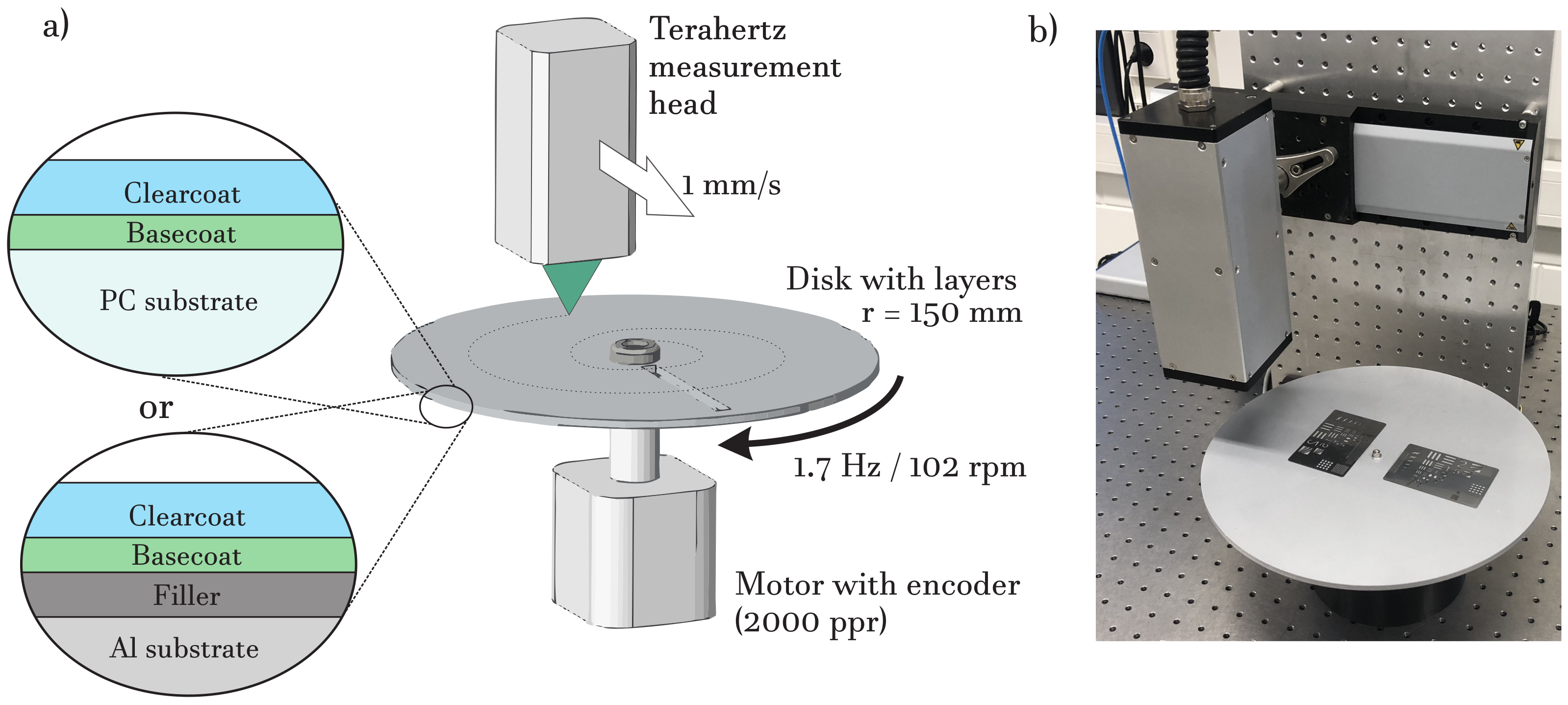
The optical configuration consists of a standard terahertz reflection setup: The terahertz emitter and detector modules [
18,
19,
20] are mounted in a compact assembly (“terahertz measurement head”, see
Figure 1), where four off-axis parabolic mirrors with a diameter of 25.4 mm guide the beam onto the sample under test and back onto the receiver. The divergent terahertz radiation from the emitter is collimated using an off-axis parabolic mirror with an effective focal length (EFL) of 50.8 mm. A second mirror with an EFL of 101.6 mm focuses the radiation onto the sample surface. After reflection, another pair of mirrors with EFLs of 101.6 mm and 50.8 mm, respectively, recollimates the beam and focuses it onto the detector.
The samples consist of metallic (aluminum) and non-metallic (polycarbonate) disks, each with a diameter of 300 mm, that are spray-coated by hand so that multiple layers are added. An aluminum mask with six cutouts serves to imprint a predefined structure in one of the layers. To this end, the first layer on each sample is produced in two steps: First, a uniform layer is applied without any mask and then, after a short drying phase of approx. 10 min, a second layer of the same coating is added, now with the chopper-blade-like mask in place. These steps imprint a “negative” of the mask in the thickness of the first layer. This artificial feature in the thickness of the layer permits a visual consistency check of the thickness results.
In the example of the metallic disk, the second and third layer features a metallic base coat and a clear coat, respectively. In contrast, the non-metallic disk is only coated with the metallic base coat and the clear coat, omitting the filler layer.
Imaging of the sample is realized in a fashion similar to the setup of Beck et al. [
21], where a sample was measured while it was both spinning and being translated. Slightly modifying this concept, we use a spinning sample together with a translation of the measurement head. The disk sample is mounted on a stepper motor with a rotation encoder providing 2000 increments per turn. Given the dimensions of the disks, this corresponds to a spatial resolution of about 0.47 mm on the outside of the disk and even less for smaller radii. The measurement head itself is mounted on an additional linear stage that radially moves the focal point of the terahertz beam across the disk. The combination of the two stages yields a spiral trajectory for terahertz imaging. In the measurements presented below, the linear axis moves at 1 mm/s, while the disk rotates at 1.7 Hz. Hence, the tangential speed amounts to 1.6 m/s at the outer circumference of the disk. The distance between successive measurement points is 1 mm and decreases correspondingly towards the center of the disk.
3. Results
3.1. Terahertz Performance
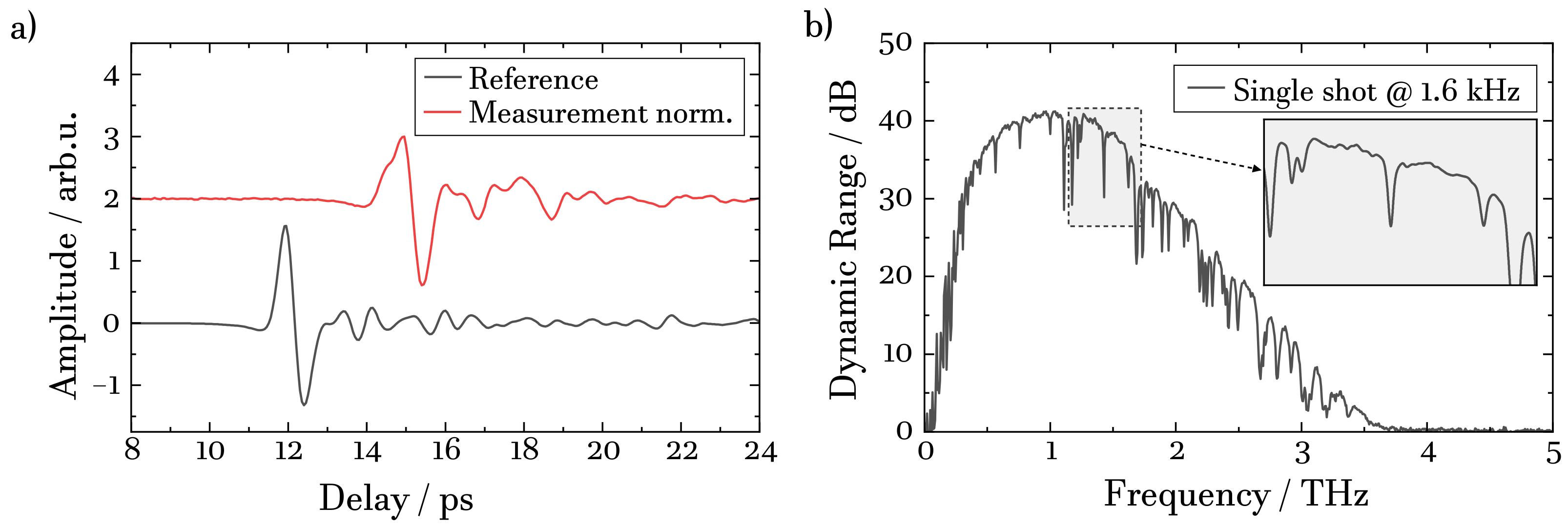
Two representative waveforms—a reference waveform and a normalized sample waveform of the three-layer-system—are shown in
Figure 2a. The sample waveform already indicates the sub-wavelength nature of the applied layers, as the echoes of the individual layers overlap and are not readily separated by the eye. The acquired waveforms comprise a time interval of about 160 ps (not fully shown in
Figure 2a), which would be sufficient for measuring samples even of millimeter thicknesses. Admittedly, the paint layers investigated in this study have a thickness of the order of a few 10 µm. Nevertheless, the 160 ps range allows for measuring samples even in applications where the distance from the measurement head to the sample surface varies by as much as ∼20 mm (as long as the Rayleigh length of the utilized optics is sufficient as well). This can be particularly useful when measuring the thicknesses of multilayer foils or webs in production.
The single-shot dynamic range of the ECOPS system is shown in
Figure 2b. The peak dynamic range of 40 dB is measured at a frequency of about 1 THz. The useable bandwidth exceeds 3 THz. These values, obtained at the full measurement rate of 1.6 kHz, are sufficient for evaluating multilayer structures [
22]. The symmetry of the water vapor absorption lines points towards the good linearity of the time axis that the ECOPS system provides. TDS systems with nonlinear time axis errors typically exhibit an amplitude overshoot at the edges of absorption lines [
23], which is not the case with the system presented.
3.2. Layer Thickness Measurements with Stationary Sample and Stationary Head
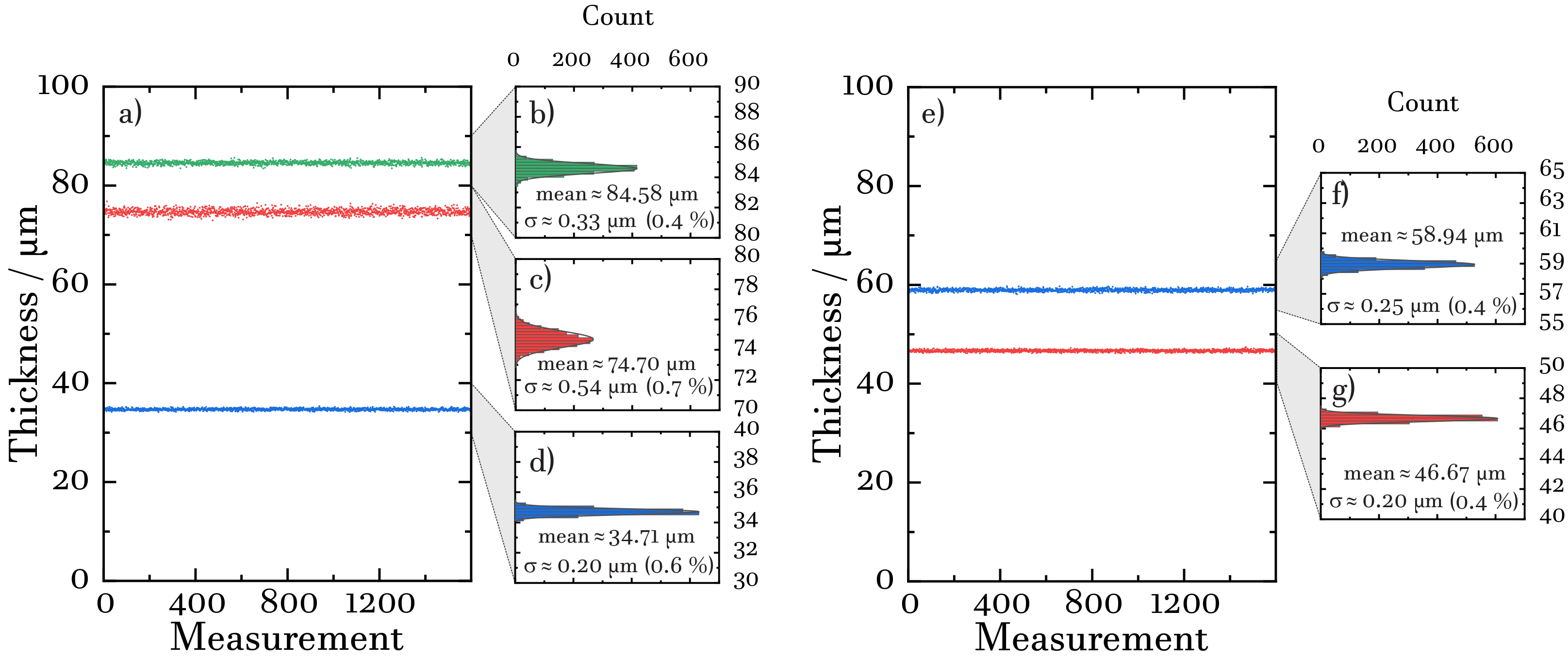
To demonstrate the stability of the measurement results, we recorded data at 1.6 kHz measurement rate with both the sample at rest and a stationary measurement head. Results for the metallic disk with three layers and the non-metallic one with two layers are shown in
Figure 3a,e, respectively. Each plot comprises 1600 data points, equivalent to a sampling time of 1 s.
Figure 3b–d as well as
Figure 3f,g show the corresponding histograms of the layer thickness results. The bin width of the histograms is 0.2 µm. The standard deviations of the individual layer thicknesses range from 0.2 µm to 0.54 µm. Hence, even at this evaluation speed, the relative error remains well below 1% for all of the individual layers investigated here.
3.3. Layer Thickness Measurements with Rotating Sample and Stationary Head
To demonstrate the repeatability of the layer thickness measurements, we present data acquired with rotating samples but stationary reflection head (fixed radius). The results of 10 consecutive turns are shown in
Figure 4. The thicknesses of all layers fall in the range of about 30 µm to 100 µm. For each sample, the polar-coordinate plots of the thickness readings overlap perfectly, which illustrates the excellent repeatability of both the raw data and the evaluation results. In the plot of the metallic substrate disk (see
Figure 4a), the slit of the disk, used for consistency checks of the image reconstruction, is seen at an angle of about 10 degrees. At an angle of 205 degrees, some deviating measurement results appear for the filler and basecoat, where the first one exhibits larger values around 110 µm and the latter one shows lower values around 30 µm. The pattern of the mask imprint is seen in the lowest layer of each sample, i.e., in the thickness of the filler in the case of the metallic substrate, and in the thickness of the base coat on the non-metallic substrate, the latter exhibiting a more pronounced and uniform thickness contrast (see
Figure 4b). This is attributed to the improved hand-spraying skills that the experimentalist developed during the project.
3.4. Layer Thickness Imaging
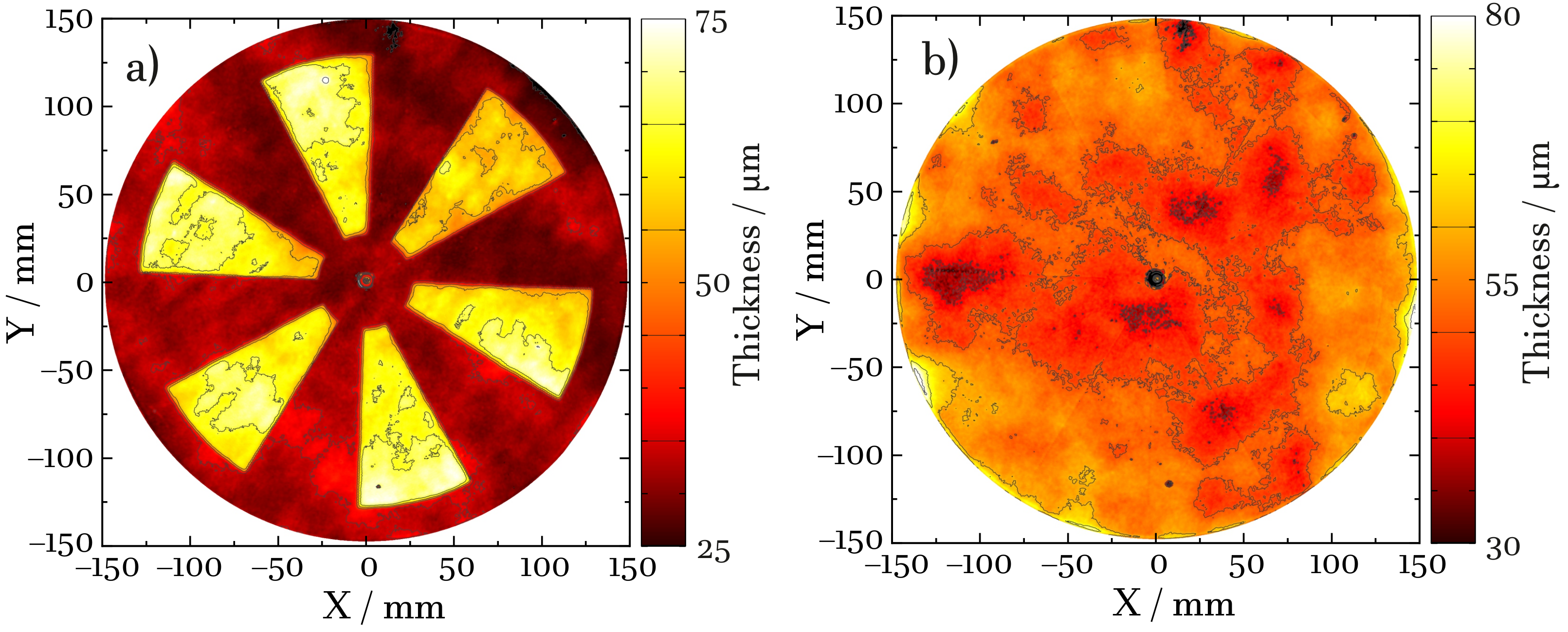
Combining the rotation of the sample with a linear translation of the measurement head as described above, we obtained terahertz images of the disk, where each pixel encodes the multilayer thickness information of its location. In the images presented in this and the following section, we use the individual layer thicknesses as contrast parameters.
Figure 5 and
Figure 6 show false-color images of the metallic disk and non-metallic disk, respectively. As expected, the structure of the mask applied to the lowest layer is mainly visible in the thickness image of exactly this layer. For the metallic substrate, the values obtained for the different layers range from 20 µm to 120 µm. The uneven distribution of values is a consequence of the hand-spraying process. The layers on the non-metallic substrate, prepared subsequently, appear more homogeneous altogether: Their values range from 25 µm to 80 µm, and the mask imprint is much more uniform, as already inferred from
Figure 4b).
3.5. Imaging of a Resolution Target
Finally, we investigated the spatial resolution of our imaging setup. Our test samples are two identical metallic resolution targets that were placed on the coated non-metallic disk and imaged with the same parameters as above. Each resolution target features laser-cut patterns of different dimensions. The numbers next to the three-stripe cutouts specify the individual stripe width in millimeters. The smallest and largest stripes are 0.1 mm and 2 mm wide, respectively.
The peak-to-peak amplitude representation of the entire image is shown in
Figure 7a. The sample layout is depicted in
Figure 7b. An enlarged section of the peak-to-peak amplitude image can be seen in
Figure 7c, where stripes down to 0.8 mm are still resolved in the intensity image.
Figure 7d–i comprise representations of the reflectivity at individual frequency ranges from 0 to 3 THz, each range covering an interval of 0.5 THz width. As expected, the resolution improves at higher frequencies, whilst the dynamic range decreases concurrently. In
Figure 7h,i, the 0.6 mm stripes are clearly seen and even the 0.4 mm stripes can be recognized.
The uniformity of the edges underlines the effectiveness of the encoder-based imaging approach: Whilst we expected the rotation speed to not be perfectly stable, the rotation encoder provides the correct position information as needed for the spatial assignment of the image pixels.
4. Discussion
The presented approach combines extremely fast terahertz imaging with quantitative measurements of layer thicknesses. A total of 240,000 pixels in total were acquired in only 2.5 min. The success of this technique is based on three different contributions: (i) the terahertz measurement system itself, where the ECOPS concept outperforms classical TDS systems by a factor of ∼100 in terms of acquisition speed; (ii) optimized retrieval algorithms that are able to analyze three-layer structures on time scales below 1 ms; and (iii) the spiral imaging trajectory. In contrast to standard raster-scan techniques, the spiral movement avoids any dead-times of the stages and hence leads to an optimized duty cycle of the measurement. The interplay of these three aspects results in a measurement rate of 1.6 kHz, which-to the best of our knowledge-represents the fastest real-time multilayer thickness measurement achieved with terahertz technologies thus far.
To test the performance of the system and in particular, the consistency and repeatability of the results, we ran tests on a static sample and obtained standard deviations below 0.6 µm. For the layer thicknesses used here, this corresponds to a relative uncertainty of less than .
We note that the data analysis algorithms work for coatings on both metallic and non-metallic substrates. Using hand-sprayed samples for our proof-of-principle study, we obtain thickness values in the range of 20 to 120 µm. We show that a mask pattern imprinted in a certain layer becomes apparent in the layer thickness plot of exactly that layer. The spatial resolution of the images presented here is given by the number of increments of the utilized rotation encoder (2000 per turn). It is slightly lower than 0.5 mm at the outer circumference of our samples, and improves with decreasing radius. Consistently, in the terahertz images obtained with standard resolution patterns, structures down to ∼0.4 mm are resolved once suitable frequency filters are applied to the “raw” intensity images.
In future implementations, a varying rotation speed and/or linear translation of the measurement head could improve the measurement time further, while keeping the resolution constant across the sample surface.
In a prospective application scenario, the measurement head itself could be equipped with a position encoder, a concept already realized in frequency-modulated continuous-wave (FMCW) terahertz imaging systems [
24]. Such a setup might operate either as a handheld thickness gauge, or could even be mounted on a robotic arm [
25]. Owing to its unmatched measurement speed, a “quantitative-imaging” system could become an invaluable aid in assessing the quality of paint layers in automotive manufacturing, or vice versa, the efficiency of a paint removal process that might become mandatory during maintenance work on aircrafts and helicopters.
5. Conclusions
We have demonstrated a terahertz imaging system that is capable of analyzing sub-wavelength layer thicknesses at kilohertz measurement rates, even in structures with two or three coating layers. The imaging setup makes use of a spiral trajectory that combines a rotating sample and a radially translated measurement head. In conjunction with an ultrafast, ECOPS-driven terahertz TDS system and optimized data analysis algorithms, we recorded signals of 240,000 pixels in 2.5 min and analyzed them in real time. Our work presents a step towards quantitative terahertz imaging, which we believe will find application in the inline quality control of coating and de-coating processes.
Author Contributions
Conceptualization, D.M., K.-S.E., J.K. and S.D.; methodology, D.M., K.-S.E., J.K. and S.D.; software, D.M., K.-S.E., J.K. and S.D.; validation, D.M., K.-S.E., J.K. and S.D.; formal analysis, D.M., K.-S.E.; investigation, D.M. and K.-S.E.; resources, D.M., J.K. and N.V.; data curation, D.M. and K.-S.E.; writing—original draft preparation, D.M., K.-S.E. and A.D.; writing—review and editing, D.M., K.-S.E., J.K., S.D., J.J., G.v.F. and A.D.; visualization, D.M. and K.-S.E.; supervision, D.M., J.J., G.v.F., N.V. and A.D.; project administration, D.M., N.V. and A.D. All authors have read and agreed to the published version of the manuscript.
Funding
This project is supported by the Federal Ministry for Economic Affairs and Climate Action (BMWK) on the basis of a decision by the German Bundestag.
Data Availability Statement
The data presented in this study are available upon reasonable request from the corresponding author.
Conflicts of Interest
The authors declare no conflict of interest.
References
- Krimi, S.; Klier, J.; Jonuscheit, J.; von Freymann, G.; Urbansky, R.; Beigang, R. Highly accurate thickness measurement of multi-layered automotive paints using terahertz technology. Appl. Phys. Lett. 2016, 109, 021105. [Google Scholar] [CrossRef]
- Naftaly, M.; Vieweg, N.; Deninger, A. Industrial applications of terahertz sensing: State of play. Sensors 2019, 19, 4203. [Google Scholar] [CrossRef] [PubMed] [Green Version]
- Ellrich, F.; Bauer, M.; Schreiner, N.; Keil, A.; Pfeiffer, T.; Klier, J.; Weber, S.; Jonuscheit, J.; Friederich, F.; Molter, D. Terahertz quality inspection for automotive and aviation industries. J. Infrared Millim. Terahertz Waves 2020, 41, 470–489. [Google Scholar] [CrossRef] [Green Version]
- van Mechelen, J.L.; Frank, A.; Maas, D.J. Thickness sensor for drying paints using THz spectroscopy. Opt. Express 2021, 29, 7514–7525. [Google Scholar] [CrossRef]
- Xu, J.; Zhang, X.C. Circular involute stage. Opt. Lett. 2004, 29, 2082–2084. [Google Scholar] [CrossRef]
- Kim, G.J.; Jeon, S.G.; Kim, J.I.; Jin, Y.S. High speed scanning of terahertz pulse by a rotary optical delay line. Rev. Sci. Instrum. 2008, 79, 106102. [Google Scholar] [CrossRef]
- Molter, D.; Ellrich, F.; Weinland, T.; George, S.; Goiran, M.; Keilmann, F.; Beigang, R.; Léotin, J. High-speed terahertz time-domain spectroscopy of cyclotron resonance in pulsed magnetic field. Opt. Express 2010, 18, 26163–26168. [Google Scholar] [CrossRef]
- Elzinga, P.A.; Lytle, F.E.; Jian, Y.; King, G.B.; Laurendeau, N.M. Pump/probe spectroscopy by asynchronous optical sampling. Appl. Spectrosc. 1987, 41, 2–4. [Google Scholar] [CrossRef]
- Bartels, A.; Thoma, A.; Janke, C.; Dekorsy, T.; Dreyhaupt, A.; Winnerl, S.; Helm, M. High-resolution THz spectrometer with kHz scan rates. Opt. Express 2006, 14, 430–437. [Google Scholar] [CrossRef] [Green Version]
- Bartels, A.; Cerna, R.; Kistner, C.; Thoma, A.; Hudert, F.; Janke, C.; Dekorsy, T. Ultrafast time-domain spectroscopy based on high-speed asynchronous optical sampling. Rev. Sci. Instrum. 2007, 78, 035107. [Google Scholar] [CrossRef] [Green Version]
- Klatt, G.; Gebs, R.; Schäfer, H.; Nagel, M.; Janke, C.; Bartels, A.; Dekorsy, T. High-resolution terahertz spectrometer. IEEE J. Sel. Top. Quantum Electron. 2010, 17, 159–168. [Google Scholar] [CrossRef] [Green Version]
- Tauser, F.; Rausch, C.; Posthumus, J.H.; Lison, F. Electronically controlled optical sampling using 100 MHz repetition rate fiber lasers. In Proceedings of the Commercial and Biomedical Applications of Ultrafast Lasers VIII, San Jose, CA, USA, 20–23 January 2008; Volume 6881, pp. 139–146. [Google Scholar]
- Kim, Y.; Yee, D.S. High-speed terahertz time-domain spectroscopy based on electronically controlled optical sampling. Opt. Lett. 2010, 35, 3715–3717. [Google Scholar] [CrossRef] [PubMed]
- Dietz, R.J.; Vieweg, N.; Puppe, T.; Zach, A.; Globisch, B.; Göbel, T.; Leisching, P.; Schell, M. All fiber-coupled THz-TDS system with kHz measurement rate based on electronically controlled optical sampling. Opt. Lett. 2014, 39, 6482–6485. [Google Scholar] [CrossRef] [PubMed]
- Yahyapour, M.; Jahn, A.; Dutzi, K.; Puppe, T.; Leisching, P.; Schmauss, B.; Vieweg, N.; Deninger, A. Fastest thickness measurements with a terahertz time-domain system based on electronically controlled optical sampling. Appl. Sci. 2019, 9, 1283. [Google Scholar] [CrossRef] [Green Version]
- Krimi, S.; Torosyan, G.; Beigang, R. Advanced GPU-based terahertz approach for in-line multilayer thickness measurements. IEEE J. Sel. Top. Quantum Electron. 2016, 23, 8501112. [Google Scholar] [CrossRef]
- Vasicek, A. Sur la réflexion de la lumière sur des verres supportant des couches minces multiples. J. Phys. Radium 1950, 11, 342–345. [Google Scholar] [CrossRef]
- Dietz, R.J.; Globisch, B.; Roehle, H.; Stanze, D.; Göbel, T.; Schell, M. Influence and adjustment of carrier lifetimes in InGaAs/InAlAs photoconductive pulsed terahertz detectors: 6 THz bandwidth and 90 dB dynamic range. Opt. Express 2014, 22, 19411–19422. [Google Scholar] [CrossRef]
- Globisch, B.; Dietz, R.; Nellen, S.; Göbel, T.; Schell, M. Terahertz detectors from Be-doped low-temperature grown InGaAs/InAlAs: Interplay of annealing and terahertz performance. AIP Adv. 2016, 6, 125011. [Google Scholar] [CrossRef] [Green Version]
- Globisch, B.; Dietz, R.; Kohlhaas, R.; Göbel, T.; Schell, M.; Alcer, D.; Semtsiv, M.; Masselink, W. Iron doped InGaAs: Competitive THz emitters and detectors fabricated from the same photoconductor. J. Appl. Phys. 2017, 121, 053102. [Google Scholar] [CrossRef]
- Beck, M.; Plötzing, T.; Maussang, K.; Palomo, J.; Colombelli, R.; Sagnes, I.; Mangeney, J.; Tignon, J.; Dhillon, S.; Klatt, G.; et al. High-speed THz spectroscopic imaging at ten kilohertz pixel rate with amplitude and phase contrast. Opt. Express 2019, 27, 10866–10872. [Google Scholar] [CrossRef]
- Weber, S.; Liebelt, L.; Klier, J.; Pfeiffer, T.; Molter, D.; Ellrich, F.; Jonuscheit, J.; Freymann, G.V. Influence of system performance on layer thickness determination using terahertz time-domain spectroscopy. J. Infrared Millim. Terahertz Waves 2020, 41, 438–449. [Google Scholar] [CrossRef] [Green Version]
- Molter, D.; Trierweiler, M.; Ellrich, F.; Jonuscheit, J.; Von Freymann, G. Interferometry-aided terahertz time-domain spectroscopy. Opt. Express 2017, 25, 7547–7558. [Google Scholar] [CrossRef] [PubMed]
- Schreiner, N.; Weber, S.; Keil, A.; Friederich, F. Mobile Handheld FMCW Terahertz Multilayer Thickness Inspection. In Proceedings of the 2019 44th International Conference on Infrared, Millimeter, and Terahertz Waves (IRMMW-THz), Paris, France, 1–6 September 2019; pp. 1–2. [Google Scholar]
- Stübling, E.M.; Rehn, A.; Siebrecht, T.; Bauckhage, Y.; Öhrström, L.; Eppenberger, P.; Balzer, J.C.; Rühli, F.; Koch, M. Application of a robotic THz imaging system for sub-surface analysis of ancient human remains. Sci. Rep. 2019, 9, 3390. [Google Scholar] [CrossRef] [PubMed] [Green Version]
| Publisher’s Note: MDPI stays neutral with regard to jurisdictional claims in published maps and institutional affiliations. |
© 2022 by the authors. Licensee MDPI, Basel, Switzerland. This article is an open access article distributed under the terms and conditions of the Creative Commons Attribution (CC BY) license (https://creativecommons.org/licenses/by/4.0/).


 ,
, 


