
GaN-on-Si: Monolithically Integrated All-GaN Drivers for High-Voltage DC-DC Power Conversion


Department of Mechanical Engineering, College of Engineering, Chang Gung University, Taoyuan 33302, Taiwan
*
Author to whom correspondence should be addressed.
Appl. Sci. 2022, 12(10), 5109; https://0-doi-org.brum.beds.ac.uk/10.3390/app12105109
Submission received: 15 April 2022
/
Revised: 12 May 2022
/
Accepted: 13 May 2022
/
Published: 19 May 2022
(This article belongs to the Special Issue Robustness and Reliability of GaN Technology in Power Switching Applications)
Abstract
:Featured Application
High-efficiency and fast power switches with low-latency driver stages have been demonstrated using GaN HEMTs on Si. Through this monolithic integration technology, high-voltage DC-DC converters can achieve high conversion efficiency at high switching frequencies.
Abstract
This paper presents a novel integrated half-bridge driver architecture using GaN-on-Si process for high-speed and high-voltage DC-DC converters. The entire circuit includes only enhancement mode (E-mode) and depletion-mode (D-mode) GaN transistors. The high-side driver circuit adopts the E-stacked E/D-mode (EED) architecture, which can directly drive the gate of the high-side transistor with a low-voltage signal without using an additional level shifter, which simplifies the design and reduces propagation delay. In addition, the low-side power transistor is driven by stacking two D/E-mode devices. This architecture separates the high-side pulse from the low-side drive signal to prevent false triggering of the low-side driver. The designed fully integrated GaN driver can output a high-voltage pulse wave with an operating frequency greater than 1 MHz when the input voltage is greater than 200 V. The rise and fall times of the high-voltage pulse wave operating at a peak voltage of 200 V are 54.4 ns and 57.6 ns, respectively. The experimental results show that the circuit can effectively drive the half-bridge circuit and be applied to a buck converter. The designed buck converter can deliver up to 20.5 W of output power, and the maximum efficiency achieves 90.7%.
1. Introduction
Gallium nitride (GaN) is considered the most promising semiconductor technology for high frequency and high power applications [1,2,3,4,5]. The unique properties of GaN materials with high breakdown electric field (4 MV/cm), large band gap (3.4 eV), and low parasitics enable the fabrication of higher speed and larger voltage swing devices, which are a great advantage for designing power converters. For example, most buck converters use a half-bridge topology due to their simple and practical design structure. Many commercial DC-DC converters use silicon (Si) power devices as switching elements, but the switching frequency is limited to a few hundred kilohertz [6,7,8,9,10]. As the switching frequency increases, the losses associated with the output capacitance of the Si device increase and reduce efficiency. On the other hand, the demand to reduce the size of the overall converter system, especially the miniaturization of passive components, requires the system to operate at higher switching frequencies. The use of fully integrated GaN power transistors and their drivers greatly addresses this challenge. In addition to exploiting the low parasitics of GaN to enable high-speed switching and improve the response speed of the system, the increase in power density has resulted in a more reliable solution compared to traditional silicon-based or other compound semiconductors [11,12,13]. In much of the past work, silicon-based drivers for high-speed GaN power transistors were widely designed to implement high-speed and high-voltage power converters [14,15,16,17,18]. Since GaN devices and drivers are based on different processing technologies, packaging becomes a challenge. Each type of package will have leads that introduce parasitic inductance. These parasitics can cause switching losses, ringing, and reliability issues when power transistors are switched at high slew-rates of tens to hundreds of volts per nanosecond. Specially treated package types can also limit the switching performance of GaN FETs [17,18]. However, integrating GaN power transistors and drivers for a half bridge in a single chip still poses many difficulties [19]. One of the main challenges is the implementation of high-side gate drivers. The high-side gate driver must turn on and off efficiently when its source switches at the full input voltage swing. Furthermore, short propagation delays and good matching are necessary for half-bridge operation at high frequencies to control gate slew rate, limit overshoot voltage and shoot-through current of power transistors. Meeting these conditions enables a high-performance integrated driver with electromagnetic interference (EMI) compliance. Various integrated gate driver designs have been reported in the literature. Normally-off or E-mode power transistors are preferred power stages for power converter applications as they provide a safe startup mode to reduce energy consumption in the driver stage. However, the design of integrated drivers using only E-mode transistors is challenging. Since there are no mature complementary devices in the existing GaN process, E-mode transistors must be designed in conjunction with on-chip resistors or diodes, which not only increases the area but also has greater uncertainty in the design results. Currently, the design of combined D-mode and E-mode GaN devices has, therefore, become a common solution [20,21,22]. However, while combining these two devices in the driver stage, one must pay special attention to leakage and overdrive design issues to ensure robust and efficient operation of high-voltage GaN power switches.
A high switching frequency of 10 MHz and high-efficiency integrated drivers have been demonstrated for D-mode power switches [23]. Integrated E-mode gate drivers with GaN-HEMTs for MHz switching operation on more expensive GaN-on-SOI substrates have been validated for low-side drivers [24,25,26]. For the GaN-on-Si process, there are currently no economical integrated high-side drivers for DC-DC converter applications. To efficiently drive E-mode GaN transistors as output stages of power converters, this paper proposes an EED inverter-based high-side driver to directly drive GaN power transistors on the GaN-on-Si process. Rather than relying solely on a conventional level shifter combined with a bootstrap circuit scheme, the EED structure modifies the D/E-mode inverter to achieve a high-efficiency and low-EMI high-side gate driver for E-mode power transistors. Through the driver design principle proposed in this paper, the high-voltage GaN power switch can operate at frequencies greater than 1 Mhz, the switching voltage exceeds 200 V, and the waveform has no overshoot at turn-on and no oscillation at turn-off, indicating that the design effectively drives high-voltage E-mode power transistors. The experimental results show that the rise and fall times of a 200 V switching pulse generated by the half-bridge driver based on EED architecture are 54.4 ns and 57.6 ns, respectively. The driver has been verified in a buck converter, and the overall efficiency of the system can reach more than 90% under the output power of 8~15 W, and the overall power consumption of the EED driver is about 0.4~0.6 W.
2. GaN-on-Si Process
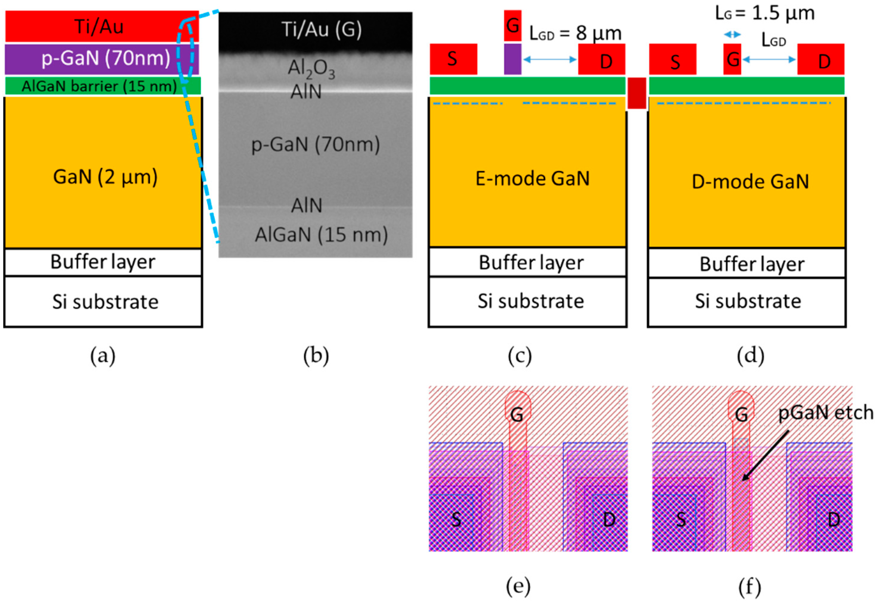
In this study, the power device and their drivers were implemented using E/D-mode transistors on the same low-resistance (<2 ohm-cm) silicon substrate. Figure 1a shows the device structure, where the AlGaN/GaN epitaxy consists of an AlGaN buffer layer, a 2 μm GaN buffer and channel layer, a 15 nm AlGaN barrier layer, and a 70 nm p-GaN stack on a Si substrate. AlN is grown on the top and bottom of p-GaN as buffer layers, and metal is grown on the top as a contact layer. Figure 1b shows an SEM photograph of part of the device structures. Figure 1c,d present the E/D-mode transistors, respectively, while Figure 1e,f show their masking layouts. From Figure 1f, the D-mode transistor can be obtained by directly etching away the p-GaN layer under the same process. Table 1 summarizes the performance of p-GaN/AlGaN/GaN HEMTs with gate lengths of LG = 1.5 μm, LGS = 5 μm, LGD = 8 μm, and gate width of 100 μm. The reasons for the variation of device parameters in the table are mainly due to the growth temperature of AlGaN and p-GaN between samples, as well as slight differences in the etching process, resulting in different surface roughness and defects, which, in turn, affect the threshold voltage and conduction current of the devices.
3. The Proposed Gate Driver for Buck Converter
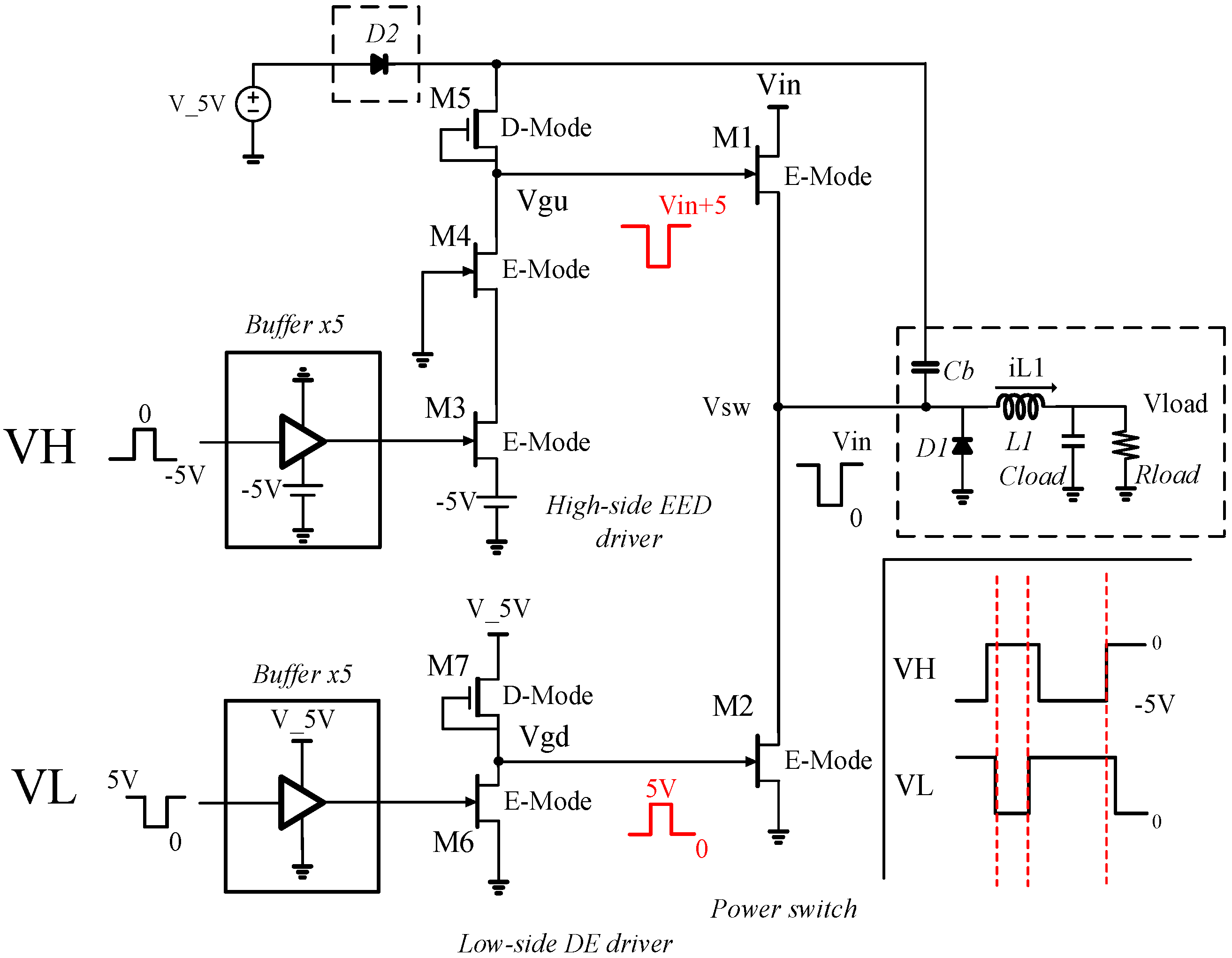
Figure 2 illustrates the proposed integrated buck converter architecture using the high-voltage GaN process, which mainly consists of three parts, namely the power switch, gate driver, and buffer stage.
3.1. Power Switch
The high-voltage power switch consists of two stacked E-mode transistors. After a trade-off analysis of switching frequency and conduction loss, the gate width of each device was set at 96 mm, consisting of 2 transistors of each 96 fingers with a width of 1000 μm.
3.2. Gate Driver
As shown in Figure 2, the high-side gate driver consists of stacked E-mode and E/D-mode GaN transistors, and an off-chip bootstrap capacitor, Cb, is also employed to increase the holding voltage when the high-side transistor is turned on. The lowest voltage of the driver was chosen to be −5 V in order to completely turn off the GaN power transistor, M1, with low threshold voltages. The low-side driver employs a conventional D/E stacking architecture [21].
The overall operation of the gate driver can be expressed as follows. In the beginning switching period, after VH turns on M3 through the buffer stage, M4 is turned on. At this moment, the gate voltage of M1 is quickly pulled down low close to −5 V and M1 is turned off. The external freewheeling diode, D1, is then turned on, and the voltage at the Vsw node is pulled down low. Then, VL can turn off M6 through the buffer stage, and the 5 V voltage source charges M2 through M7. While M2 is turned on, in addition to increase the falling speed of Vsw, the bootstrap capacitor, Cb is also charged to 5 V. In the later switching period, when VL turns on M6, M2 is turned off and then VH can turn off M3. After that, the charged Cb can directly pull up the gate of M1 through M5, and M1 turns on to pull up Vsw high to charge the output inductor L1 for one complete cycle. Since the low-side power switch is switched on/off complementarily after the high-side switch through the dead-time control, the on-time of VH and VL can be set to avoid the shoot-through current of the two GaN power transistors. M4 can be designed using GaN transistors with longer LGD to increase resistance to high voltage switching at the gate node of M1, Vgu. Conversely, M3 can use GaN transistors with shorter LGD to increase switching speed.
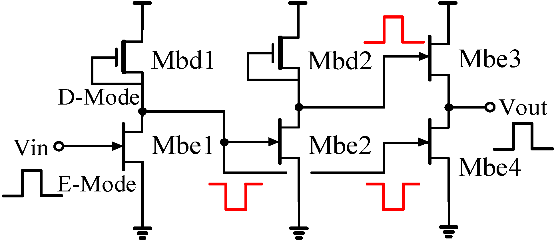
3.3. Buffer Stage
The buffer stage design uses three stages of stacked inverters in series [23]. The first two stages are D/E stacked inverters, and the last stage is E/E stacked inverters. In order to ensure low overshoot and low power consumption at output, the size of D-mode transistors is designed to be small. Table 2 summarizes the device size of the converter.
4. Experimental Results
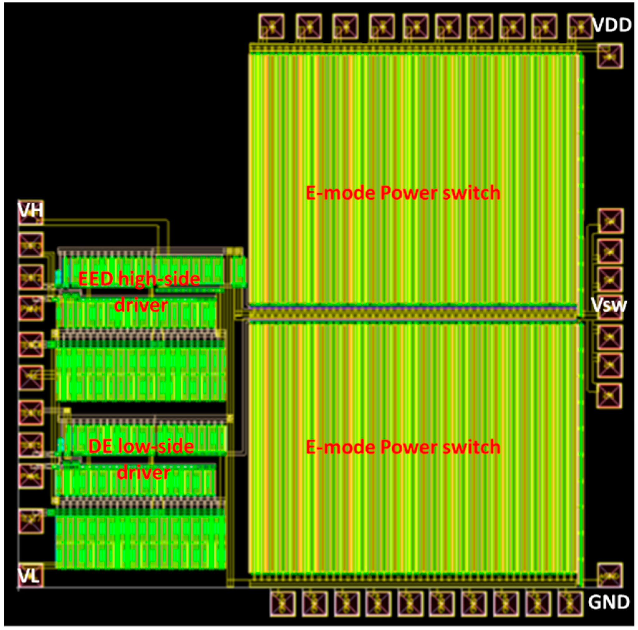
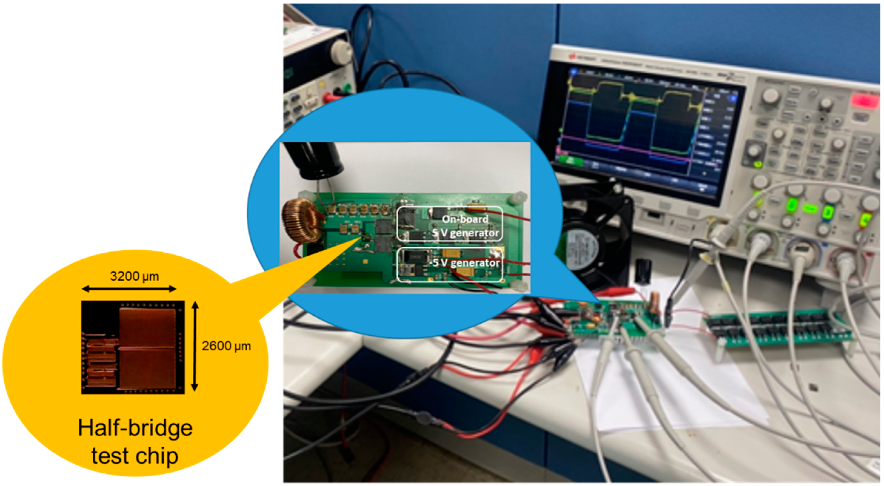
The masking layout of GaN half-bridge, integrated with high- and low-side gate-drivers using the same process, is shown in Figure 4. The chip area is 3.2 × 2.6 mm2. Around 2/3 of the die area is filled with power transistors.
The die photo and experimental set up for the buck converter are shown in Figure 5. The auxiliary power supplies of 5 V and −5 V were generated from the input voltage and integrated on the same PCB board to evaluate the overall system efficiency. The parameters of the components are listed in Table 3.
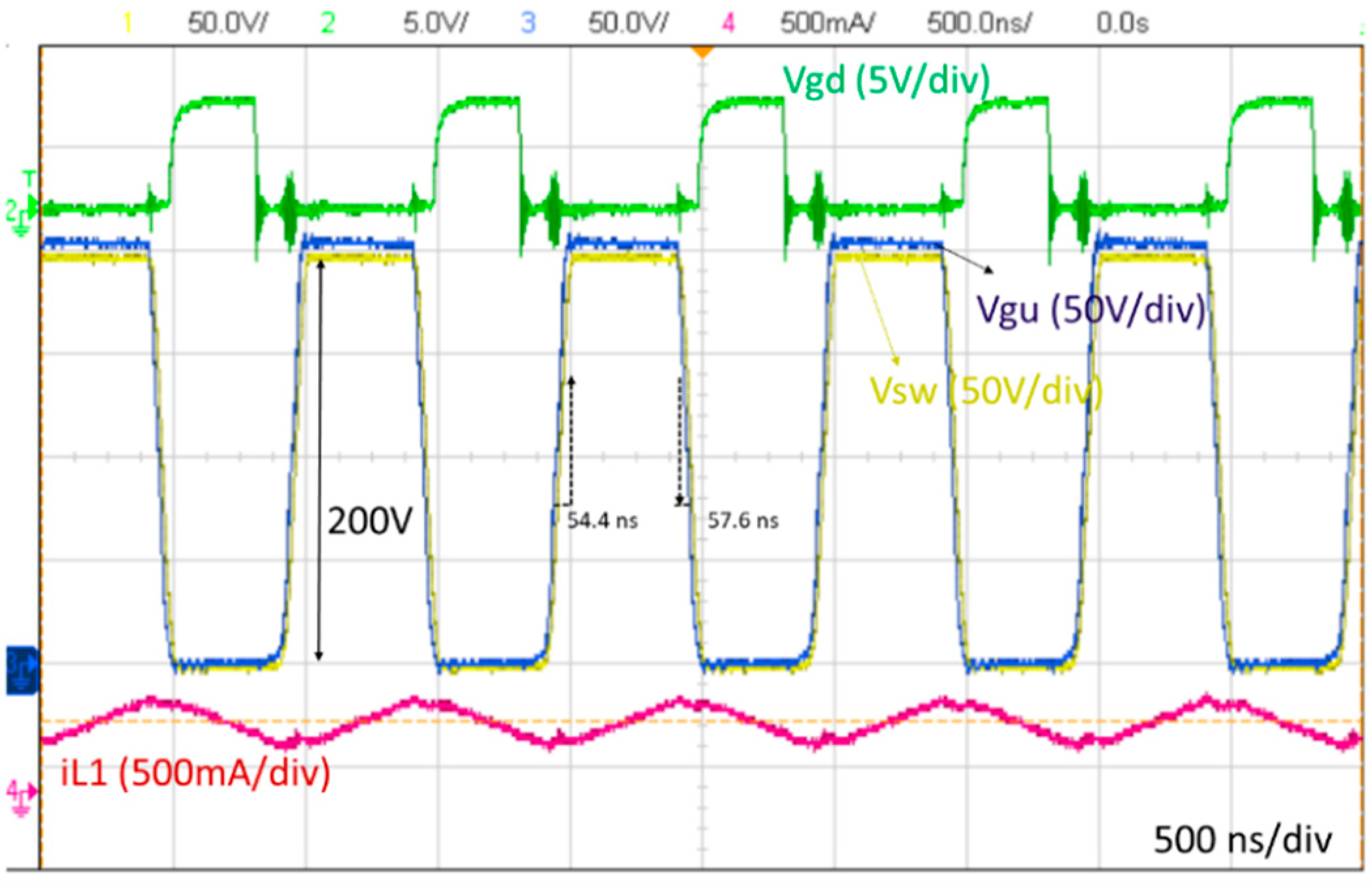
Figure 6 shows the switching waveforms of the IC tested in buck mode with a drive signal switching frequency of 1 MHz, a duty cycle set to 50%, and an input voltage of 200 V. The gate voltage, Vgd, of the low-side driver is slightly affected by the high-side driver during the rise/fall of Vsw. However, no overshoot or ringing was observed in Vsw, even though the high-side gate voltage, Vgu, exceeds the input voltage due to bootstrapping. The rise and fall times of the 200 V switching pulse are 54.4 ns and 57.6 ns, respectively. Table 4 compares the performance of high-speed GaN drivers with the latest published work using Si-based technology. Our implementation demonstrates high voltage operation for such an application, and ease of integration with power devices.
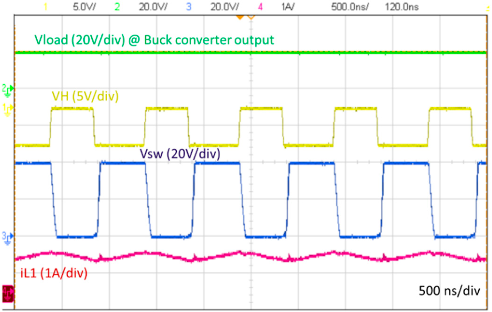
The efficiency performance of the designed buck converter was measured under the following conditions. The load is from 19 to 160 ohms, 1 MHz drive signal and its duty cycle is set to 49~51%, and the input DC voltage is given 40 V, the auxiliary voltage is 5 V and −5 V, respectively. Figure 7 shows one of the measured output voltages of the converter and the switching waveforms. The propagation delay between VH (high-to-low) and Vsw (low-to-high) is less than 10 ns. The output voltage of the buck is close to 20 V DC as expected.
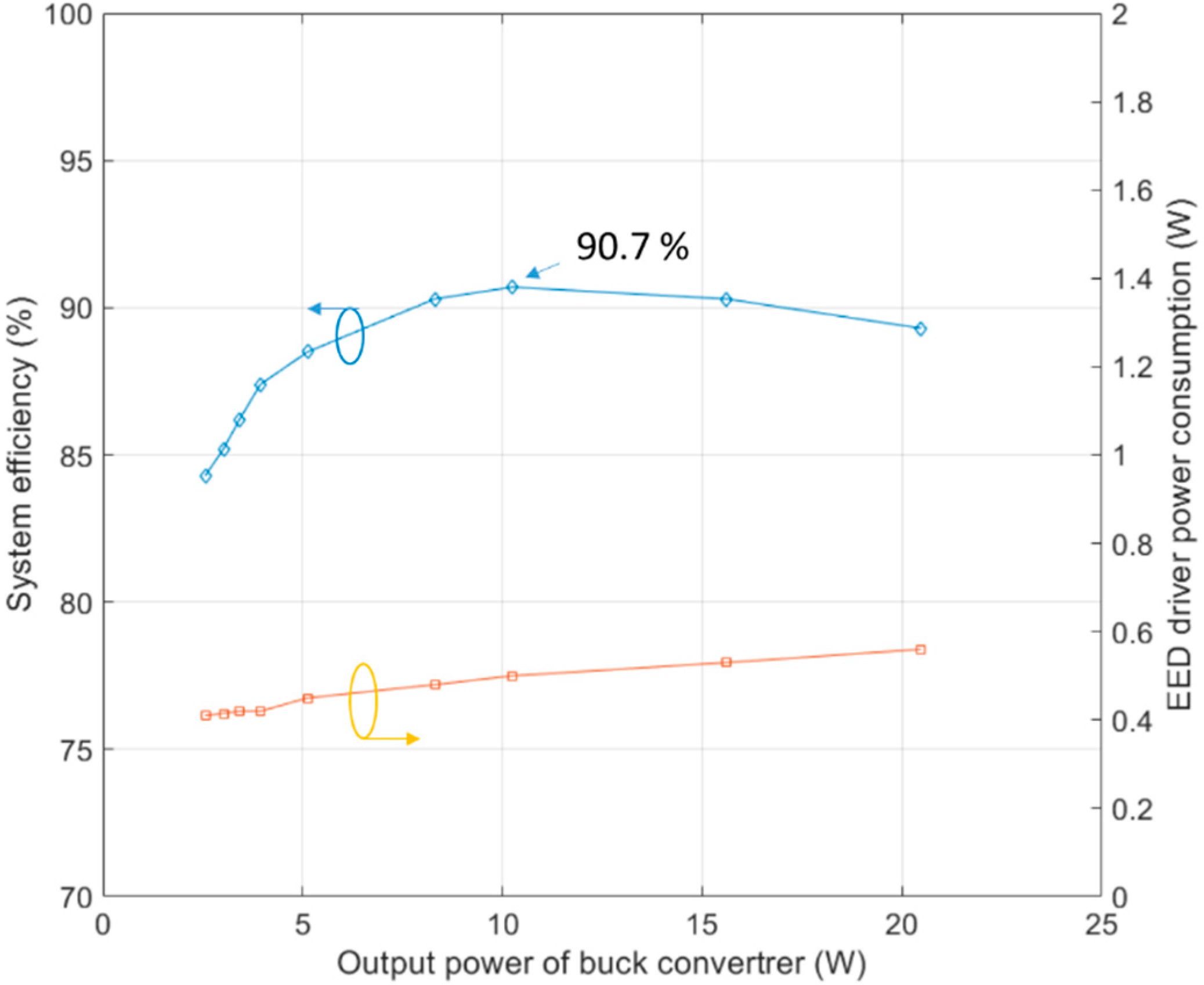
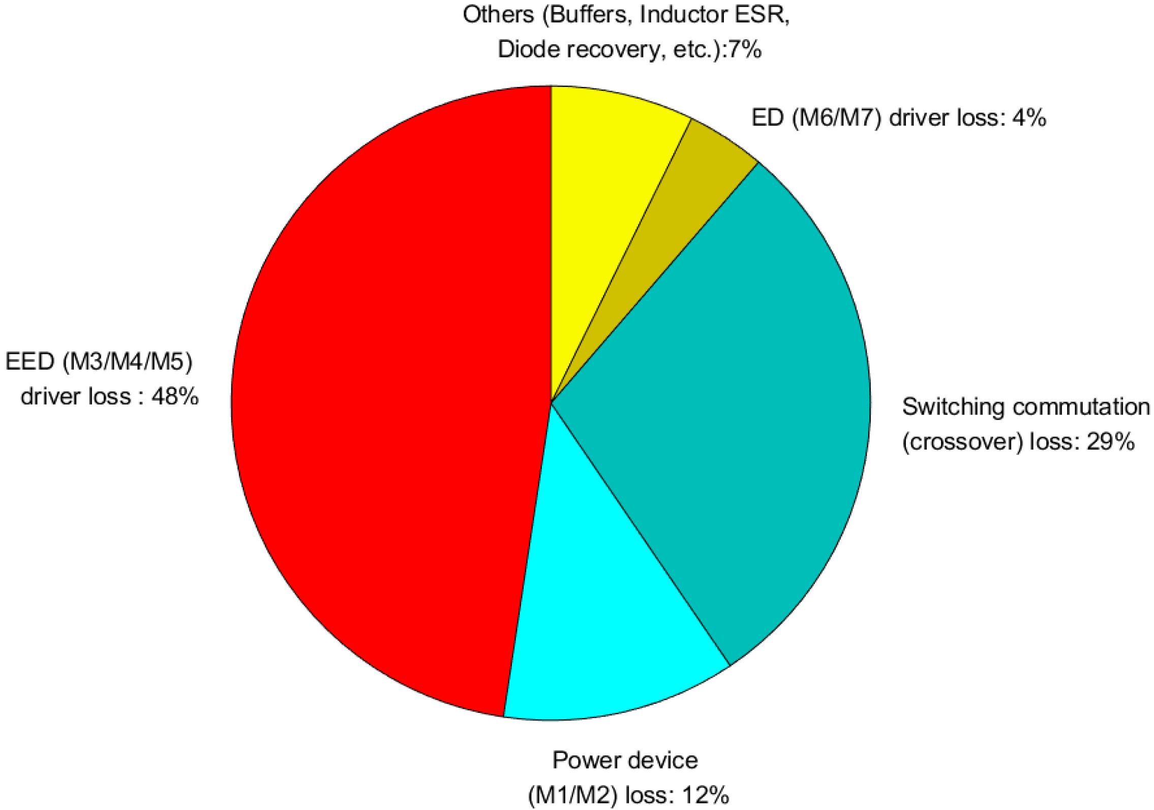
System efficiency is calculated as the ratio of DC output power to DC input power. The measured DC power consumption of the EED driver and the system efficiency of the buck converter are shown in Figure 8. When the output power exceeds 8 W, the efficiency of the system exceeds 90%. Due to the shoot−through current inside the EED driver from the 5 V to −5 V supply when M1 is off, the power consumption will increase slightly as the load becomes heavier. The measured DC power dissipation is about 0.4 to 0.6 W, which accounts for most of the power loss in the buck converter. After efficiency analysis [27], the conduction loss and output capacitance loss of the GaN power devices is about 124 mW. This shows another advantage of using GaN as a switch for high-speed switching power converters. The crossover loss of the hard-switched converter is estimated to be about 307 mW under a 40 ohm resistive load. Figure 9 shows a pie chart of the estimated percentage power loss for each device in the converter at 90.7% efficiency. Table 5 summarizes the integrated buck converter performance with other previously published works. Our implementation exhibits high efficiency at 8 to 15 W output power, and this architecture can be extended to high power switching converters with better package support.
5. Discussions
This article discusses a high-side driver circuit architecture for integrated half-bridge designs, primarily for buck converters, including device characteristics, circuit operation, and implementation issues. One of the advantages of the proposed driver is that it does not require the traditional level shifters typically employed in half-bridge designs. It is easier for engineers to adjust the delay of input drive signals to avoid possible shoot-through current that can occur in the output power switches, particularly operating at high switching frequencies. The architecture has been validated for a buck converter with maximum output power around 20 W, and efficiency achieves about 90% over a wide load range. From the above results, there remains some areas for improvement in this architecture. First, the EED/ED driver still has leakage issues when the high-side power switch is turned off, making the overall power consumption about 0.6 W. This can be improved from a power consumption perspective, resizing the driver and reducing losses in the EED/ED driver. Secondly, the package selection can be further studied for higher power applications to avoid thermal problems and thereby increase the output power of the overall system.
6. Conclusions
A fully integrated buck converter and its drivers are implemented in the GaN-on-Si process using 1.5 μm E/D mode GaN HEMTs. The rise and fall times of high-voltage switching signals operating at 200 V peak voltage are 54.4 ns and 57.6 ns, respectively. Output DC power of the designed buck converter ranges from 8 to 15 W with more than 90% efficiency over a wide range of output loads. The experimental results indicate that the designed integrated half-bridge can be well used in high-speed power converters.
Author Contributions
Conceptualization, C.H.; methodology, C.H.; validation, D.-F.L. and C.H.; formal analysis, C.H.; investigation, C.H.; data curation, D.-F.L.; writing—original draft preparation, C.H.; writing—review and editing, C.H.; revision, C.H.; project administration, C.H.; funding acquisition, C.H. All authors have read and agreed to the published version of the manuscript.
Funding
This research has been supported by the Ministry of Science and Technology, Taiwan, R.O.C., grant number MOST 110-2218-E-182-012-.
Institutional Review Board Statement
Not applicable.
Informed Consent Statement
Not applicable.
Data Availability Statement
Not applicable.
Acknowledgments
The authors would like to express their appreciations for Yu-Ming Hsin of the National Central University for the valuable discussions on GaN device modeling, measurement and GaN device fabrication support, and Taiwan Semiconductor Research Institute (TSRI) for device and system assembly support.
Conflicts of Interest
The authors declare no conflict of interest.
References
- Koyama, M.; Ikeda, K.; Takao, K. Novel cascode GaN module integrated a single gate driver IC with high switching speed controllability. In Proceedings of the 20th European Conference on Power Electronics and Applications (EPE’18 ECCE Europe), Riga, Latvia, 17–21 September 2018; pp. P.1–P.8. [Google Scholar]
- Lin, T.C.; Hsia, C. Integrated Linear Regulator for GaN-based Gate Driver Applications. In Proceedings of the IEEE 4th International Future Energy Electronics Conference (IFEEC), Singapore, 25–28 November 2019. [Google Scholar] [CrossRef]
- Wei, J.; Zhang, M.; Lyu, G.; Chen, K.J. Substrate Effects in GaN-on-Si Integrated Bridge Circuit and Proposal of Engineered Bulk Silicon Substrate for GaN Power ICs. In Proceedings of the IEEE Workshop on Wide Bandgap Power Devices and Applications in Asia (WiPDA Asia), Suita, Japan, 23–25 September 2020. [Google Scholar] [CrossRef]
- Li, S.T.; Wang, P.Y.; Chen, C.J.; Hsu, C. A 10 MHz GaN Based Buck Converter with Dynamic Pull-up Resistor Gate Driver. In Proceedings of the IEEE 4th International Future Energy Electronics Conference (IFEEC), Singapore, 25–28 November 2019. [Google Scholar] [CrossRef]
- Zhou, D.C.; Chiu, H.C.; Zhang, J.; Wong, R.K.-Y.; Zhao, T.; Zhang, F.; Zhang, M.; Zou, Y.; Chen, L. A Massive Adoption Ready 200 mm 40 V–650 V E-mode GaN-on-Si Power HEMTs Technology. In Proceedings of the IEEE Applied Power Electronics Conference and Exposition (APEC), New Orleans, LA, USA, 15–19 March 2020; pp. 636–639. [Google Scholar] [CrossRef]
- Alaql, F.; Alhatlani, A.; Batarseh, I. Multi-Mode Rectifier-Based LLC Resonant Converter for Wide Input Voltage Range Applications. In Proceedings of the IEEE Applied Power Electronics Conference and Exposition (APEC), Phoenix, AZ, USA, 14–17 June 2021; pp. 349–354. [Google Scholar] [CrossRef]
- Ming, X.; Fan, Z.; Xin, Y.; Zhang, X.; Shi, F.; Pan, S.; Zhang, J.; Wang, Z.; Zhang, B. An Advanced Bootstrap Circuit for High Frequency, High Area-Efficiency and Low EMI Buck Converter. IEEE Trans. Circuits Syst. II Express Briefs 2019, 66, 858–862. [Google Scholar] [CrossRef]
- Zhu, L.; Li, C.; Yang, H.; Yan, H.; Li, W.; He, X. Buck-Boost Type High Voltage DC Auxiliary Power Supply for Medium Voltage DC System. In Proceedings of the IEEE 1st International Power Electronics and Application Symposium (PEAS), Shanghai, China, 12–15 November 2021. [Google Scholar] [CrossRef]
- Alaql, F.; Alluhaybi, K.; Batarseh, I. A Wide Input Voltage Range LLC Converter with Multi-mode Operations. In Proceedings of the IEEE 9th International Power Electronics and Motion Control Conference (IPEMC2020-ECCE Asia), Shanghai, China, 12–15 November 2021; pp. 1710–1715. [Google Scholar] [CrossRef]
- Park, I.; Maeng, J.; Shim, M.; Jeong, J.; Kim, C. A Bidirectional High-Voltage Dual-Input Buck Converter for Triboelectric Energy-Harvesting Interface Achieving 70.72% End-to-End Efficiency. In Proceedings of the 2019 Symposium on VLSI Circuits, Kyoto, Japan, 9–14 June 2019; pp. c326–c327. [Google Scholar] [CrossRef]
- Ke, X.; Ma, D.B. A 3-to-40V VIN 10-to-50 MHz 12W Isolated GaN Driver with Self-Excited dead Minimizer Achieving 0.2ns/0.3ns tdead, 7.9% Minimum Duty Ratio and 50V/ns CMTI. In Proceedings of the Solid-State Circuits Conference–(ISSCC) IEEE International, San Francisco, CA, USA, 11–15 February 2018; pp. 386–388. [Google Scholar] [CrossRef]
- Seidel, A.; Wicht, B. A fully integrated three-level 11.6nC gate driver supporting GaN gate injection transistors. In Proceedings of the Solid—State Circuits Conference—(ISSCC) IEEE International, San Francisco, CA, USA, 11–15 February 2018; pp. 384–386. [Google Scholar] [CrossRef]
- Xue, L.; Zhang, J. Active clamp flyback using GaN power IC for power adapter applications. In Proceedings of the IEEE Applied Power Electronics Conference and Exposition (APEC), Tampa, FL, USA, 26–30 March 2017; pp. 2441–2448. [Google Scholar] [CrossRef]
- Ke, X.; Yan, D.; Sankman, J.; Song, M.K.; Ma, D.B. A 3-to-40-V Automotive-Use GaN Driver with Active Bootstrap Balancing and VSW Dual-Edge Dead-Time Modulation Techniques. IEEE J. Solid-State Circuits 2021, 56, 521–530. [Google Scholar] [CrossRef]
- Yan, R.; Xi, J.; He, L. A 2–10 MHz GaN HEMTs Half-Bridge Driver with Bandgap Reference Comparator Clamping and Dual Level Shifters for Automotive Applications. IEEE Trans. Ind. Electron. 2019, 67, 1446–1454. [Google Scholar] [CrossRef]
- Chen, C.-J.; Chiu, P.-K.; Chen, Y.-M.; Wang, P.-Y.; Chang, Y.-C. An Integrated Driver with Adaptive Dead-Time Control for GaN-Based Synchronous Buck Converter. IEEE Trans. Circuits Syst. II Express Briefs 2022, 69, 539–543. [Google Scholar] [CrossRef]
- Zhang, W.J.; Yu, J.; Cui, W.T.; Leng, Y.; Liang, J.; Hsieh, Y.-T.; Tsai, H.-H.; Juang, Y.-Z.; Yeh, W.-K.; Ng, W.T. A Smart Gate Driver IC for GaN Power HEMTs with Dynamic Ringing Suppression. IEEE Trans. Power Electron. 2021, 36, 14119–14132. [Google Scholar] [CrossRef]
- Yang, C.; Chen, W.; Fan, Y.; Gui, P. Design and Characterization of a 10-MHz GaN Gate Driver Using On-Chip Feed-Forward Gaussian Switching Regulation for EMI Reduction. IEEE J. Solid-State Circuits 2021, 56, 3521–3532. [Google Scholar] [CrossRef]
- Lin, W.; Chatterjee, U.; Martinez, W. Characterization of Enhancement-Mode Asymmetrical GaN Transistor Half Bridge in High Frequency Operation. In Proceedings of the 2021 23rd European Conference on Power Electronics and Applications (EPE’21 ECCE Europe), Ghent, Belgium, 6–10 September 2021; pp. P1–P7. [Google Scholar]
- Cui, M.; Sun, R.; Bu, Q.; Liu, W.; Wen, H.; Li, A.; Liang, Y.C.; Zhao, C. Monolithic GaN Half-Bridge Stages with Integrated Gate Drivers for High Temperature DC-DC Buck Converters. IEEE Access 2019, 7, 184375–184384. [Google Scholar] [CrossRef]
- Kaufmann, M.; Lueders, M.; Kaya, C.; Wicht, B. 18.2 A Monolithic E-Mode GaN 15W 400V Offline Self-Supplied Hysteretic Buck Converter with 95.6% Efficiency. In Proceedings of the IEEE International Conference on Solid-State Circuits (ISSCC), San Francisco, CA, USA, 16–20 February 2020; pp. 288–290. [Google Scholar] [CrossRef]
- Noike, S.; Nagao, J.; Furuta, J.; Kobayashi, K. An Asynchronous Buck Converter by Using a Monolithic GaN IC Integrated by an Enhancement-Mode GaN-on-SOI Process. In Proceedings of the 2021 IEEE 8th Workshop on Wide Bandgap Power Devices and Applications (WiPDA), Redondo Beach, CA, USA, 7–11 November 2021; pp. 215–219. [Google Scholar] [CrossRef]
- Telliez, I.; Nakatani, T. 95% Efficiency 10 MHz Switching Rate and 30 W, Fully Integrated Buck Converters Using E/D-mode GaN HEMTs, Dtic.Mil Report; Defense Technical Information Center: Fort Belvoir, VA, USA, 2019; pp. 501–505. [Google Scholar]
- Yamashita, Y.; Stoffels, S.; Posthuma, N.; Decoutere, S.; Kobayashi, K. Monolithically Integrated E-mode GaN-on-SOI Gate Driver with Power GaN-HEMT for MHz-Switching. In Proceedings of the 2018 IEEE 6th Workshop on Wide Bandgap Power Devices and Applications (WiPDA), Atlanta, GA, USA, 31 October–2 November 2018; pp. 231–236. [Google Scholar] [CrossRef]
- Murray, S.K.; Jiang, W.L.; Zaman, M.S.; De Vleeschouwery, H.; Moensy, P.; Roigy, J.; Trescases, O. On-Chip Dynamic Gate-Voltage Waveform Sampling in a 200-V GaN-on-SOI Power IC. IEEE J. Emerg. Sel. Top. Power Electron. 2022. Early Access. [Google Scholar] [CrossRef]
- Cosnier, T.; Syshchyk, O.; de Jaeger, B.; Geens, K.; Cingu, D.; Fabris, E.; Borga, M.; Vohra, A.; Zhao, M.; Bakeroot, B.; et al. 200 V GaN-on-SOI Smart Power Platform for Mono-lithic GaN Power ICs. In Proceedings of the 2021 IEEE International Electron Devices Meeting (IEDM), San Francisco, CA, USA, 11–16 December 2021; pp. 5.1.1–5.1.4. [Google Scholar] [CrossRef]
- Application Note: Efficiency of Buck Converter, ROHM Semiconductor. 2016. Available online: https://fscdn.rohm.com/en/products/databook/applinote/ic/power/switching_regulator/buck_converter_efficiency_app-e.pdf (accessed on 5 May 2022).
Figure 1.
High-voltage GaN device structure (a), the SEM cross-sectional view of the device (b), the E-mode GaN profile (c), the D-mode GaN profile (d), masking layout of the E-mode GaN device (e), and masking layout of the D-mode GaN device (f).
Figure 1.
High-voltage GaN device structure (a), the SEM cross-sectional view of the device (b), the E-mode GaN profile (c), the D-mode GaN profile (d), masking layout of the E-mode GaN device (e), and masking layout of the D-mode GaN device (f).

Figure 2.
The proposed integrated buck converter using high−voltage GaN process. The components in the dash box are off-chip.
Figure 2.
The proposed integrated buck converter using high−voltage GaN process. The components in the dash box are off-chip.

Figure 3.
The buffer stage design.

Figure 4.
The masking layout of the integrated GaN half-bridge and its driver.

Figure 5.
Die photo and test setup for the integrated buck converter (Auxiliary power supplies are on board).
Figure 5.
Die photo and test setup for the integrated buck converter (Auxiliary power supplies are on board).

Figure 6.
Measured switching waveforms and inductor current at 1 Mhz input drive signal.

Figure 7.
The half-bridge operated with Vin = 40 V, iL1_avg = 1 A, Vsw switching at 1 MHz and ~50% duty cycle.
Figure 7.
The half-bridge operated with Vin = 40 V, iL1_avg = 1 A, Vsw switching at 1 MHz and ~50% duty cycle.

Figure 8.
Overall system efficiency of buck converter and EED driver power consumption versus output power at switching frequency of 1 MHz.
Figure 8.
Overall system efficiency of buck converter and EED driver power consumption versus output power at switching frequency of 1 MHz.

Figure 9.
Overall power loss percentage comparison of an EED−driven GaN-based buck converter at 1 MHz switching frequency to achieve a maximum efficiency of 90.7%.
Figure 9.
Overall power loss percentage comparison of an EED−driven GaN-based buck converter at 1 MHz switching frequency to achieve a maximum efficiency of 90.7%.


Table 1.
Performance summary of p-GaN/AlGaN/GaN HEMT.
| Parameter | E-Mode | D-Mode |
|---|---|---|
| Threshold voltage (Vt) @ Id = 1 mA/mm) | 0.9~1.5 | −10~−7 |
| gm_max (mS/mm) | 67~88 | - |
| Ron (Ω-mm) @ Vds = 6 V | 14~19 | 13~15 |
| Ids_max (mA/mm) | 277~295 | 300~360 |
| M1/M2 | M3 | M4 | M5 | M6 | M7 | Mbd1 | Mbe1 | Mbd2 | Mbe2 | Mbe3/Mbe4 | |
|---|---|---|---|---|---|---|---|---|---|---|---|
| E-mode (mm) | 96 | 1.2 | 1.2 | 1.2 | 0.04 | 0.1 | 0.8/0.8 | ||||
| D-mode (mm) | 0.08 | 0.08 | 0.02 | 0.04 |
Table 3.
Circuit parameter for the buck converter.
| Parameter | |
|---|---|
| Vin (V) | 30~200 |
| Switching frequency (MHz) | 0.5~2 |
| Output inductor: L1 (μH) | 25~100 |
| Output capacitor, Cload (μF) | 5 |
| Output load, Rload (Ω) | 19~160 |
Table 4.
Performance comparisons between different types of high-speed GaN drivers.
| Parameter | [14] | [15] | [18] | This Work |
|---|---|---|---|---|
| Structure | Active BST balancing | BGRCC | Current-mode (SSFD + GR) | EED |
| Technology | Si-based | Si-based | BCD | GaN on Si |
| Switching frequency (MHz) | 10~30 | 2~10 | 10 | >=1 |
| Level-shifter | Yes | Yes | Yes | No |
| Slew-rate (V/μs) | 26 K | 1.8 K | 5.7 K | 3.7 K |
| Maximum operating voltage (V) | 40 | 18 | 40 | 200 |
Table 5.
Buck converter performance comparisons using integrated driver solutions.
| Parameter | [21] | [22] | [23] | This Work |
|---|---|---|---|---|
| Architecture | Offline Buck | Asynchronous Buck | Synchronous Buck | Synchronous Buck |
| Technology | GaN on Si | GaN on SOI | D-mode RF GaN on SiC | E-mode GaN on Si |
| Switching frequency (MHz) | 0.262 | 1~2 | 10 | >=1 |
| Max. output power (W) | 15 | 24 | 10 | 20.5 |
| Max. Efficiency (%) | 95.6 | 89.8 | 95 | 90.7 |
Publisher’s Note: MDPI stays neutral with regard to jurisdictional claims in published maps and institutional affiliations. |
© 2022 by the authors. Licensee MDPI, Basel, Switzerland. This article is an open access article distributed under the terms and conditions of the Creative Commons Attribution (CC BY) license (https://creativecommons.org/licenses/by/4.0/).
Share and Cite
MDPI and ACS Style
Hsia, C.; Lu, D.-F. GaN-on-Si: Monolithically Integrated All-GaN Drivers for High-Voltage DC-DC Power Conversion. Appl. Sci. 2022, 12, 5109. https://0-doi-org.brum.beds.ac.uk/10.3390/app12105109
AMA Style
Hsia C, Lu D-F. GaN-on-Si: Monolithically Integrated All-GaN Drivers for High-Voltage DC-DC Power Conversion. Applied Sciences. 2022; 12(10):5109. https://0-doi-org.brum.beds.ac.uk/10.3390/app12105109
Chicago/Turabian StyleHsia, Chin, and Deng-Fong Lu. 2022. "GaN-on-Si: Monolithically Integrated All-GaN Drivers for High-Voltage DC-DC Power Conversion" Applied Sciences 12, no. 10: 5109. https://0-doi-org.brum.beds.ac.uk/10.3390/app12105109
Note that from the first issue of 2016, this journal uses article numbers instead of page numbers. See further details here.